EP1300948B1 - Sehr schneller Amplitudenspitzenwertvergleicher - Google Patents
Sehr schneller Amplitudenspitzenwertvergleicher Download PDFInfo
- Publication number
- EP1300948B1 EP1300948B1 EP02254838A EP02254838A EP1300948B1 EP 1300948 B1 EP1300948 B1 EP 1300948B1 EP 02254838 A EP02254838 A EP 02254838A EP 02254838 A EP02254838 A EP 02254838A EP 1300948 B1 EP1300948 B1 EP 1300948B1
- Authority
- EP
- European Patent Office
- Prior art keywords
- signal
- transistor
- source
- input
- peak amplitude
- Prior art date
- Legal status (The legal status is an assumption and is not a legal conclusion. Google has not performed a legal analysis and makes no representation as to the accuracy of the status listed.)
- Expired - Lifetime
Links
- 239000003990 capacitor Substances 0.000 claims description 15
- 238000000034 method Methods 0.000 claims description 7
- 230000005669 field effect Effects 0.000 claims description 4
- 238000005516 engineering process Methods 0.000 description 3
- 229910001218 Gallium arsenide Inorganic materials 0.000 description 2
- 238000004891 communication Methods 0.000 description 2
- 238000001514 detection method Methods 0.000 description 2
- 238000012986 modification Methods 0.000 description 2
- 230000004048 modification Effects 0.000 description 2
- 230000005540 biological transmission Effects 0.000 description 1
- 238000001914 filtration Methods 0.000 description 1
- RGNPBRKPHBKNKX-UHFFFAOYSA-N hexaflumuron Chemical compound C1=C(Cl)C(OC(F)(F)C(F)F)=C(Cl)C=C1NC(=O)NC(=O)C1=C(F)C=CC=C1F RGNPBRKPHBKNKX-UHFFFAOYSA-N 0.000 description 1
- 229910044991 metal oxide Inorganic materials 0.000 description 1
- 150000004706 metal oxides Chemical class 0.000 description 1
- 230000003362 replicative effect Effects 0.000 description 1
- 229910052710 silicon Inorganic materials 0.000 description 1
- 239000010703 silicon Substances 0.000 description 1
- 230000009897 systematic effect Effects 0.000 description 1
Images

Classifications
-
- H—ELECTRICITY
- H03—ELECTRONIC CIRCUITRY
- H03K—PULSE TECHNIQUE
- H03K5/00—Manipulating of pulses not covered by one of the other main groups of this subclass
- H03K5/153—Arrangements in which a pulse is delivered at the instant when a predetermined characteristic of an input signal is present or at a fixed time interval after this instant
- H03K5/1532—Peak detectors
-
- G—PHYSICS
- G01—MEASURING; TESTING
- G01R—MEASURING ELECTRIC VARIABLES; MEASURING MAGNETIC VARIABLES
- G01R19/00—Arrangements for measuring currents or voltages or for indicating presence or sign thereof
- G01R19/04—Measuring peak values or amplitude or envelope of AC or of pulses
Definitions
- the present invention relates in general to integrated circuitry, and in particular to various implementations for a high speed peak amplitude comparator.
- FIG. 1 depicts a typical implementation for a conventional peak amplitude detector 100.
- An amplifier 102 and transistor M1 are connected in a feedback configuration with the input signal Vin being applied to one input of amplifier 102.
- Vin rises and transistor M1 turns on, the amplitude of the signal Vc (at node 104) essentially follows that of Vin.
- Vc When Vin drops from its peak value, transistor M1 turns off, but capacitor C1 maintains the charge at node 104 at the peak value of Vc. Thus, the amplitude of the signal Vc always reflects the peak amplitude of Vin.
- a current source 10 is provided to allow capacitor C1 to discharge in case of random glitches at the input. Current I0 is made very small relative to the size of capacitor C1. As long as an input signal is present, Vin updates the charge stored by capacitor C1 thus the slow discharge does not result in an appreciable reduction in Vc in the absence of a glitch.
- a drawback of the circuit of Figure 1 is that because of the feedback loop its speed of operation is limited. Thus, for very high speed applications such as data communication circuitry in the GigaHz range (e.g., SONET OC192), peak detectors with this type of feedback loop are not suitable. This has created a need for peak amplitude detection circuit techniques that are operable at very high frequencies.
- the present invention provides various methods and circuits for implementing high speed peak amplitude comparison. Broadly, the invention achieves higher speed of operation by eliminating the slow feedback loop commonly employed in peak detection.
- the invention directly compares a signal that represents the peak amplitude of the input signal minus a small voltage drop to a modified reference voltage.
- the modified reference voltage corresponds to the reference voltage that is adjusted to compensate for the small voltage drop in the maximum input voltage. As thus constructed, a comparison of the two voltages performs the intended function without the need for a feedback loop.
- the invention implements a differential version of the peak amplitude comparator to obtain better noise rejection and reduced effective offset among other advantages.
- the present invention provides a peak amplitude comparator including an input circuit having an input terminal coupled to receive an input signal, and configured to generate at an output terminal a first signal with an amplitude that is substantially equal to a peak amplitude of the input signal minus a predetermined voltage drop; a reference circuit having an input terminal coupled to receive a reference voltage and configured to generate at an output terminal a second signal with an amplitude that is substantially equal to the reference voltage minus the predetermined voltage drop; and a comparator having a first terminal coupled to receive the first signal and a second terminal coupled to receive the second signal.
- the input circuit includes: a transistor having a gate terminal couple to receive the input signal, a first source/drain terminal coupled to a logic high power supply and a second source/drain terminal coupled to the output terminal of the input circuit; a capacitor coupled to the second source/drain terminal of the transistor; and a current source coupled to the second source/drain terminal of the transistor, wherein the predetermined voltage drop is substantially equal to a threshold voltage of the transistor.
- the present invention provides a differential peak amplitude comparator including an input circuit having first and second input terminals coupled to respectively receive differential first and second input signals, and configured to generate at an output terminal a first signal with an amplitude that is substantially equal to a peak amplitude of either of the first and second input signals minus a predetermined voltage drop; a reference circuit having an input terminal coupled to receive a reference voltage and configured to generate at an output terminal a second signal with an amplitude that is substantially equal to the reference voltage minus the predetermined voltage drop; and a comparator having a first terminal coupled to receive the first signal and a second terminal coupled to receive the second signal.
- the present invention provides a method for comparing a peak amplitude of an input signal to a reference voltage, including storing on a first node a first signal having an amplitude that is substantially equal to a peak amplitude of the input signal minus a predetermined voltage drop; applying to a second node a second signal with an amplitude that is substantially equal to the reference voltage minus the predetermined voltage drop; and comparing a magnitude of the first signal to a magnitude of the second signal.
- Figure 1 depicts a typical circuit implementation for a conventional peak detector
- Figure 2 is a simplified circuit schematic for an exemplary implementation of a peak amplitude comparator according to one embodiment of the present invention
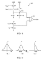
- Figure 3 is a simplified circuit schematic for an exemplary implementation of a differential peak amplitude comparator according to another embodiment of the present invention.
- Figures 4A, 4B and 4C illustrate the offset behavior of the various embodiments of peak amplitude detectors and comparators described herein.
- Peak amplitude comparator 200 includes an input circuit (or input path) 202 and a reference circuit (or reference path) 204.
- Input circuit 202 includes a field effect transistor M2 that receives the input signal Vin at its gate terminal.
- Transistor M2 has its drain terminal connected to the positive power supply VDD and its source terminal connected to node 206.
- a capacitor C2 connects between node 206 and ground (or negative power supply VSS depending on the implementation).
- a current source device I1 connects in parallel with capacitor C2 and provides a discharge path for capacitor C2 to address glitch conditions at the input.
- Reference circuit 204 includes a field effect transistor M3 that receives a reference signal Vref at its gate terminal. Transistor M3 has its drain terminal connected to VDD and its source terminal connected to node 208.
- a current source device I2, preferably replicating current source device I1 connects between the source terminal of transistor M3 and ground.
- a comparator 210 receives node 206 at one input and node 208 at another. The output of comparator 210 provides the output OUT of the circuit.
- Current source devices I1 and I2 may be implemented by a transistor that has its gate driven by a bias voltage.
- transistors M2 and M3 may be connected to another voltage, and possibly coupled to VDD via another circuit element such as a resistor.
- some applications may include filtering such as an RC low pass filter at node 206.
- Vin turns on transistor M2 when its magnitude is one Vth greater than the signal level at its source terminal (node 206), where Vth is the threshold voltage of transistor M2.
- Vth is the threshold voltage of transistor M2.
- Reference circuit 204 includes a circuit that essentially replicates input circuit 202.
- Vref is applied to the gate terminal of transistor M3, and transistor M3 is biased by current source 12.
- Signal V2 at the source terminal of transistor M3 is thus equal to Vref-Vth where Vth is the threshold voltage of transistor M3.
- This circuit can operates at much higher frequencies compared to the prior art peak detectors of the type shown in Figure 1.
- the present invention provides a differential implementation for a peak amplitude comparator.
- Figure 3 is a simplified circuit schematic for an exemplary implementation of a differential peak amplitude comparator 300 according to this embodiment of the present invention.
- Circuit 300 is similar to the single-ended circuit of Figure 2 in most respects except for the inclusion of a second transistor in the input path.
- the circuit includes a first transistor M4 that receives the positive half Vinp of the differential input signal and a second transistor M5 that receives the negative half Vinn of the differential input signal.
- Figure 3 also shows the use of transistors M7 and M8 each having its gate driven by a bias voltage Vb as the current source devices. It is to be understood that other types of implementations for current source devices are possible.
- the current source can be implemented using resistors or cascode connected transistors, and the like.
- Another advantage of the differential peak amplitude comparator of Figure 3 is a significant reduction in offset.
- the high speed input signal that is received from the transmission line is typically amplified before it is applied to the peak amplitude comparator.
- Transistor mismatch and amplifier systematic offset as well as offset inherent in the differential signal contribute to the DC offset Vos.
- Differences between the input path and the reference path as well as transistor mismatch in the comparator (304) also add to the DC offset Vos.
- the magnitude and sign of this offset signal Vos varies from chip to chip and depends on the input signal to the chip. Its distribution can be approximated by a bell shaped curve centered around zero as shown in Figure 4A.
- the peak value of Vinp (i.e., Vinpmax) is also a bell shaped curve with it s center at the ideal value when the offset signal Vos equal zero as shown in Figure 4B.
- Vinpmax is reduced but Vinnmax is increased, and the peak value becomes [Viomax+ Vos ], where Viomax is the ideal peak value (with no offset) of both Vinp and Vinn. That is, with the differential implementation shown in Figure 3, the two-sided offset distribution is rectified to only the positive side as shown in Figure 4C. This leads to a direct reduction in the range of the peak value that is impacted by offset.
- the present invention thus provides method and circuitry for implementing high speed peak amplitude comparators.
- Two specific embodiments, one single-ended and one differential implementations, have been described wherein peak comparison is accomplished without the need for a feedback loop.
- MOSFET metal-oxide field effect transistor
- the illustrative embodiments shown in Figures 2 and 3 employ metal-oxide field effect transistor (MOSFET) technology.
- MOSFET metal-oxide field effect transistor
- the present invention is not limited to MOSFET technology and other technologies such as bipolar, GaAs or GaAs on silicon and the like may be used to implement the present invention.
- the scope of the present invention is thus not limited to the specific embodiments described, and is instead defined by the following claims.
Landscapes
- Physics & Mathematics (AREA)
- Nonlinear Science (AREA)
- Manipulation Of Pulses (AREA)
- Measurement Of Current Or Voltage (AREA)
Claims (11)
- Spitzenamplitudenwertvergleicher, welcher aufweist:eine Eingangsschaltung mit einem Eingangsanschluss, der so gekoppelt ist, dass er ein Eingangssignal empfängt, und so konfiguriert ist, dass er an einem Ausgangsanschluss ein erstes Signal mit einer Amplitude erzeugt, die im Wesentlichen gleich einer Spitzenamplitude des Eingangssignals minus einen vorgegebenen Spannungsabfall ist;eine Bezugsschaltung mit einem Eingangsanschluss, der so gekoppelt ist, dass er eine Bezugsspannung empfängt, und so konfiguriert ist, dass er an einem Ausgangsanschluss ein zweites Signal mit einer Amplitude erzeugt, die im Wesentlichen gleich der Bezugsspannung minus den vorgegebenen Spannungsabfall ist; undeinen Komparator mit einem ersten Anschluss, der so gekoppelt ist, dass er das erste Signal empfängt, und einem zweiten Anschluss, der so gekoppelt ist, dass er das zweite Signal empfängt.
- Spitzenamplitudenwertvergleicher nach Anspruch 1, wobei der vorgegebene Spannungsabfall im Wesentlichen gleich einer Transistor-Schwellwertspannung ist.
- Spitzenamplitudenwertvergleicher nach den Ansprüchen 1 oder 2, wobei die Eingangsschaltung aufweist:einen ersten Transistor mit einem Gate-Anschluss, der so gekoppelt ist, dass er das Eingangssignal empfängt, einem ersten Source/Drain-Anschluss, der mit einer Logisch Hoch-Leistungsversorgung gekoppelt ist, und einem zweiten Source/Drain-Anschluss, der mit dem Ausgangsanschluss der Eingangsschaltung gekoppelt ist;einen Kondensator, der mit dem zweiten Source/Drain-Anschluss des ersten Transistors gekoppelt ist; undeine Stromquelle, die mit dem zweiten Source/Drain-Anschluss des ersten Transistors gekoppelt ist, wobei der vorgegebene Spannungsabfall im Wesentlichen gleich einer Schwellwertspannung des ersten Transistors ist.
- Spitzenamplitudenwertvergleicher nach einem der Ansprüche 1 bis 3, wobei die Bezugsschaltung aufweist:einen zweiten Transistor mit einem Gate-Anschluss, der so gekoppelt ist, dass er das Bezugssignal empfängt, einem ersten Source/Drain-Anschluss, der mit der Logisch Hoch-Leistungsversorgung gekoppelt ist, und einem zweiten Source/Drain-Anschluss, der mit dem Ausgangsanschluss der Bezugsschaltung gekoppelt ist; undeine Stromquelle, die mit dem zweiten Source/Drain-Anschluss des zweiten Transistors gekoppelt ist.
- Spitzenamplitudenwertvergleicher nach Anspruch 4, wobei der erste Transistor und der zweite Transistor jeweils einen Feldeffekttransistor aufweisen.
- Spitzenamplitudenwertvergleicher nach Anspruch 1, wobei das Eingangssignal ein erstes und ein zweites Differentialsignal aufweist, und der Eingangsanschluss einen ersten und einen zweiten Anschluss aufweist, die so gekoppelt sind, dass sie das erste bzw. das zweite Differentialsignal empfangen.
- Spitzenamplitudenwertvergleicher nach Anspruch 6, wobei die Eingangsschaltung aufweist:einen ersten Transistor mit einem Gate-Anschluss, der so gekoppelt ist, dass er das erste Differentialsignal empfängt, einem ersten Source/Drain-Anschluss, der mit einer Logisch Hoch-Leistungsversorgung gekoppelt ist, und einem zweiten Source/Drain-Anschluss, der mit dem Ausgangsanschluss der Eingangsschaltung gekoppelt ist;einen zweiten Transistor mit einem Gate-Anschluss, der so gekoppelt ist, dass er das zweite Differentialsignal empfängt, einem ersten Source/Drain-Anschluss, der mit der Logisch Hoch-Leistungsversorgung gekoppelt ist, undeinem zweiten Source/Drain-Anschluss, der mit dem Ausgangsanschluss der Eingangsschaltung gekoppelt ist;einen Kondensator, der mit den zweiten Source/Drain-Anschlüssen des ersten und des zweiten Transistors gekoppelt ist; undeine Stromquelle, die mit den zweiten Source/Drain-Anschlüssen des ersten und des zweiten Transistors gekoppelt ist.
- Spitzenamplitudenwertvergleicher nach Anspruch 7, wobei der vorgegebene Spannungsabfall im Wesentlichen gleich einer Schwellwertspannung des ersten Transistors ist.
- Verfahren zum Vergleichen einer Spitzenamplitude eines Eingangssignals mit einer Bezugsspannung, welches umfasst:Speichern an einem ersten Knoten eines ersten Signals mit einer Amplitude, die im Wesentlichen gleich einer Spitzenamplitude des Eingangssignals minus einen vorgegebenen Spannungsabfall ist;Erzeugen eines zweiten Signals mit einer Amplitude, die im Wesentlichen gleich der Bezugsspannung minus den vorgegebenen Spannungsabfall ist; undVergleichen einer Größe des ersten Signals mit einer Größe des zweiten Signals.
- Verfahren nach Anspruch 9, wobei der Schritt des Speicherns umfasst:Einschalten eines Schalters zum Laden eines Kondensators, wenn die Amplitude des Eingangssignals zunimmt; undAbschalten des Schalters, wenn das Eingangssignal abzunehmen beginnt.
- Verfahren nach Anspruch 10, wobei die Schritte des Einschaltens und Abschaltens des Schalters das direkte Anlegen des Eingangssignals an einen Steueranschluss des Schalters umfassen.
Applications Claiming Priority (2)
| Application Number | Priority Date | Filing Date | Title |
|---|---|---|---|
| US09/969,837 US6888381B2 (en) | 2001-10-01 | 2001-10-01 | High speed peak amplitude comparator |
| US969837 | 2001-10-01 |
Publications (3)
| Publication Number | Publication Date |
|---|---|
| EP1300948A2 EP1300948A2 (de) | 2003-04-09 |
| EP1300948A3 EP1300948A3 (de) | 2004-02-11 |
| EP1300948B1 true EP1300948B1 (de) | 2006-09-06 |
Family
ID=25516057
Family Applications (1)
| Application Number | Title | Priority Date | Filing Date |
|---|---|---|---|
| EP02254838A Expired - Lifetime EP1300948B1 (de) | 2001-10-01 | 2002-07-10 | Sehr schneller Amplitudenspitzenwertvergleicher |
Country Status (3)
| Country | Link |
|---|---|
| US (3) | US6888381B2 (de) |
| EP (1) | EP1300948B1 (de) |
| DE (1) | DE60214493T2 (de) |
Families Citing this family (9)
| Publication number | Priority date | Publication date | Assignee | Title |
|---|---|---|---|---|
| US7571511B2 (en) * | 2002-01-03 | 2009-08-11 | Irobot Corporation | Autonomous floor-cleaning robot |
| US7276953B1 (en) * | 2003-11-12 | 2007-10-02 | Cypress Semiconductor Corporation | Level shifting input buffer circuit |
| US7348808B2 (en) * | 2005-04-27 | 2008-03-25 | Pmc-Sierra, Inc. | Method and apparatus for detection of high-speed electrical signals |
| US7956641B1 (en) | 2005-04-28 | 2011-06-07 | Cypress Semiconductor Corporation | Low voltage interface circuit |
| US20080061842A1 (en) * | 2006-09-07 | 2008-03-13 | Micron Technology, Inc. | Circuit and method for detecting timed amplitude reduction of a signal relative to a threshold voltage |
| US7560959B2 (en) * | 2006-09-18 | 2009-07-14 | Micron Technology, Inc. | Absolute value peak differential voltage detector circuit and method |
| US7782095B2 (en) * | 2007-11-26 | 2010-08-24 | Faraday Technology Corp. | Signal comparison circuit |
| JP5535608B2 (ja) * | 2009-12-21 | 2014-07-02 | ラピスセミコンダクタ株式会社 | 電圧変化検知装置 |
| DE102016100261A1 (de) * | 2016-01-08 | 2017-07-13 | Nanofocus Ag | Verfahren zur elektronischen Analyse eines zeitlichen veränderlichen Signals |
Family Cites Families (11)
| Publication number | Priority date | Publication date | Assignee | Title |
|---|---|---|---|---|
| GB1281984A (en) | 1970-03-07 | 1972-07-19 | Marconi Instruments Ltd | Improvements in or relating to peak detection circuits |
| US4866301A (en) | 1988-05-24 | 1989-09-12 | Dallas Semiconductor Corporation | Controlled slew peak detector |
| US5041795A (en) * | 1990-04-27 | 1991-08-20 | Analog Devices, Inc. | Three-terminal operational amplifier and applications thereof |
| US5189313A (en) * | 1990-11-19 | 1993-02-23 | Tektronix, Inc. | Variable transition time generator |
| JP2762868B2 (ja) * | 1992-09-29 | 1998-06-04 | 日本電気株式会社 | 電圧比較回路 |
| US5357150A (en) * | 1992-11-06 | 1994-10-18 | International Business Machines Corporation | Defect tolerant envelope follower |
| US5302863A (en) * | 1993-01-29 | 1994-04-12 | Hewlett-Packard Company | CMOS peak amplitude detector |
| US5631584A (en) | 1995-09-29 | 1997-05-20 | Dallas Semiconductor Corporation | Differential cross coupled peak detector |
| US5942921A (en) * | 1997-12-19 | 1999-08-24 | Advanced Micro Devices, Inc. | Differential comparator with an extended input range |
| US6051998A (en) | 1998-04-22 | 2000-04-18 | Mitsubishi Semiconductor America, Inc. | Offset-compensated peak detector with output buffering |
| US6388477B1 (en) * | 2001-06-28 | 2002-05-14 | Sunplus Technology Col, Ltd. | Switchable voltage follower and bridge driver using the same |
-
2001
- 2001-10-01 US US09/969,837 patent/US6888381B2/en not_active Expired - Lifetime
-
2002
- 2002-07-10 EP EP02254838A patent/EP1300948B1/de not_active Expired - Lifetime
- 2002-07-10 DE DE60214493T patent/DE60214493T2/de not_active Expired - Lifetime
-
2005
- 2005-01-06 US US11/031,102 patent/US7049856B2/en not_active Expired - Lifetime
-
2006
- 2006-03-06 US US11/369,604 patent/US20060164127A1/en not_active Abandoned
Also Published As
| Publication number | Publication date |
|---|---|
| US6888381B2 (en) | 2005-05-03 |
| US7049856B2 (en) | 2006-05-23 |
| US20030062928A1 (en) | 2003-04-03 |
| DE60214493D1 (de) | 2006-10-19 |
| EP1300948A2 (de) | 2003-04-09 |
| US20050122137A1 (en) | 2005-06-09 |
| DE60214493T2 (de) | 2007-05-31 |
| US20060164127A1 (en) | 2006-07-27 |
| EP1300948A3 (de) | 2004-02-11 |
Similar Documents
| Publication | Publication Date | Title |
|---|---|---|
| US12231155B2 (en) | Peak and gain calibration of a receiver in an isolation product | |
| KR101362507B1 (ko) | 고선형 고속 피크 검출 장치 | |
| US7129782B2 (en) | Fully differential amplifier with start up circuit | |
| EP1300948B1 (de) | Sehr schneller Amplitudenspitzenwertvergleicher | |
| WO2002056558A9 (en) | Active filter circuit with dynamically modifiable internal gain | |
| IT201800010793A1 (it) | Circuito di rilevazione, dispositivo e procedimento corrispondenti | |
| US20030228024A1 (en) | Shock sound prevention circuit | |
| JP4321959B2 (ja) | 信号補償回路及び復調回路 | |
| US8487661B2 (en) | Zero-crossing gain control system and associated methods | |
| US20060208768A1 (en) | High speed peak amplitude comparator | |
| US5525934A (en) | Output circuit with short circuit protection for a CMOS comparator | |
| US11496342B1 (en) | Methods and apparatus to demodulate an input signal in a receiver | |
| CN115708324B (zh) | 包络检测 | |
| CN114362700B (zh) | 差分放大器及其背栅控制方法 | |
| US11750960B2 (en) | Shock recovery for silicon microphone systems | |
| US20240088851A1 (en) | Detection circuit, reception circuit, and semiconductor integrated circuit | |
| US5394108A (en) | Non-linear burst mode data receiver | |
| Huang et al. | A 1 V instrumentation amplifier | |
| US6775527B2 (en) | Squelch circuit with adjustable reference level | |
| US5304939A (en) | Tracking peak detector | |
| KR20000023207A (ko) | 저전력 디지털 입력 회로 |
Legal Events
| Date | Code | Title | Description |
|---|---|---|---|
| PUAI | Public reference made under article 153(3) epc to a published international application that has entered the european phase |
Free format text: ORIGINAL CODE: 0009012 |
|
| AK | Designated contracting states |
Kind code of ref document: A2 Designated state(s): AT BE BG CH CY CZ DE DK EE ES FI FR GB GR IE IT LI LU MC NL PT SE SK TR |
|
| AX | Request for extension of the european patent |
Extension state: AL LT LV MK RO SI |
|
| PUAL | Search report despatched |
Free format text: ORIGINAL CODE: 0009013 |
|
| AK | Designated contracting states |
Kind code of ref document: A3 Designated state(s): AT BE BG CH CY CZ DE DK EE ES FI FR GB GR IE IT LI LU MC NL PT SE SK TR |
|
| AX | Request for extension of the european patent |
Extension state: AL LT LV MK RO SI |
|
| RIC1 | Information provided on ipc code assigned before grant |
Ipc: 7G 01R 19/04 B Ipc: 7H 03K 5/1532 B Ipc: 7H 03K 5/08 A |
|
| 17P | Request for examination filed |
Effective date: 20040811 |
|
| AKX | Designation fees paid |
Designated state(s): DE FR GB |
|
| GRAP | Despatch of communication of intention to grant a patent |
Free format text: ORIGINAL CODE: EPIDOSNIGR1 |
|
| GRAS | Grant fee paid |
Free format text: ORIGINAL CODE: EPIDOSNIGR3 |
|
| GRAA | (expected) grant |
Free format text: ORIGINAL CODE: 0009210 |
|
| AK | Designated contracting states |
Kind code of ref document: B1 Designated state(s): DE FR GB |
|
| RAP1 | Party data changed (applicant data changed or rights of an application transferred) |
Owner name: BROADCOM CORPORATION |
|
| REG | Reference to a national code |
Ref country code: GB Ref legal event code: FG4D |
|
| REF | Corresponds to: |
Ref document number: 60214493 Country of ref document: DE Date of ref document: 20061019 Kind code of ref document: P |
|
| ET | Fr: translation filed | ||
| RAP2 | Party data changed (patent owner data changed or rights of a patent transferred) |
Owner name: BROADCOM CORPORATION |
|
| PLBE | No opposition filed within time limit |
Free format text: ORIGINAL CODE: 0009261 |
|
| STAA | Information on the status of an ep patent application or granted ep patent |
Free format text: STATUS: NO OPPOSITION FILED WITHIN TIME LIMIT |
|
| 26N | No opposition filed |
Effective date: 20070607 |
|
| REG | Reference to a national code |
Ref country code: FR Ref legal event code: CA |
|
| PGFP | Annual fee paid to national office [announced via postgrant information from national office to epo] |
Ref country code: FR Payment date: 20130719 Year of fee payment: 12 Ref country code: GB Payment date: 20130723 Year of fee payment: 12 |
|
| GBPC | Gb: european patent ceased through non-payment of renewal fee |
Effective date: 20140710 |
|
| REG | Reference to a national code |
Ref country code: FR Ref legal event code: ST Effective date: 20150331 |
|
| PG25 | Lapsed in a contracting state [announced via postgrant information from national office to epo] |
Ref country code: GB Free format text: LAPSE BECAUSE OF NON-PAYMENT OF DUE FEES Effective date: 20140710 Ref country code: FR Free format text: LAPSE BECAUSE OF NON-PAYMENT OF DUE FEES Effective date: 20140731 |
|
| PGFP | Annual fee paid to national office [announced via postgrant information from national office to epo] |
Ref country code: DE Payment date: 20160731 Year of fee payment: 15 |
|
| REG | Reference to a national code |
Ref country code: DE Ref legal event code: R082 Ref document number: 60214493 Country of ref document: DE Representative=s name: BOSCH JEHLE PATENTANWALTSGESELLSCHAFT MBH, DE Ref country code: DE Ref legal event code: R081 Ref document number: 60214493 Country of ref document: DE Owner name: AVAGO TECHNOLOGIES GENERAL IP (SINGAPORE) PTE., SG Free format text: FORMER OWNER: BROADCOM CORP., IRVINE, CALIF., US |
|
| REG | Reference to a national code |
Ref country code: DE Ref legal event code: R119 Ref document number: 60214493 Country of ref document: DE |
|
| PG25 | Lapsed in a contracting state [announced via postgrant information from national office to epo] |
Ref country code: DE Free format text: LAPSE BECAUSE OF NON-PAYMENT OF DUE FEES Effective date: 20180201 |