EP1300825A1 - Display device and its driving method, and projection-type display device - Google Patents
Display device and its driving method, and projection-type display device Download PDFInfo
- Publication number
- EP1300825A1 EP1300825A1 EP01938660A EP01938660A EP1300825A1 EP 1300825 A1 EP1300825 A1 EP 1300825A1 EP 01938660 A EP01938660 A EP 01938660A EP 01938660 A EP01938660 A EP 01938660A EP 1300825 A1 EP1300825 A1 EP 1300825A1
- Authority
- EP
- European Patent Office
- Prior art keywords
- sampling
- signal
- clock
- clock signal
- display device
- Prior art date
- Legal status (The legal status is an assumption and is not a legal conclusion. Google has not performed a legal analysis and makes no representation as to the accuracy of the status listed.)
- Withdrawn
Links
Images








Classifications
-
- G—PHYSICS
- G09—EDUCATION; CRYPTOGRAPHY; DISPLAY; ADVERTISING; SEALS
- G09G—ARRANGEMENTS OR CIRCUITS FOR CONTROL OF INDICATING DEVICES USING STATIC MEANS TO PRESENT VARIABLE INFORMATION
- G09G3/00—Control arrangements or circuits, of interest only in connection with visual indicators other than cathode-ray tubes
- G09G3/20—Control arrangements or circuits, of interest only in connection with visual indicators other than cathode-ray tubes for presentation of an assembly of a number of characters, e.g. a page, by composing the assembly by combination of individual elements arranged in a matrix no fixed position being assigned to or needed to be assigned to the individual characters or partial characters
- G09G3/34—Control arrangements or circuits, of interest only in connection with visual indicators other than cathode-ray tubes for presentation of an assembly of a number of characters, e.g. a page, by composing the assembly by combination of individual elements arranged in a matrix no fixed position being assigned to or needed to be assigned to the individual characters or partial characters by control of light from an independent source
- G09G3/36—Control arrangements or circuits, of interest only in connection with visual indicators other than cathode-ray tubes for presentation of an assembly of a number of characters, e.g. a page, by composing the assembly by combination of individual elements arranged in a matrix no fixed position being assigned to or needed to be assigned to the individual characters or partial characters by control of light from an independent source using liquid crystals
-
- G—PHYSICS
- G09—EDUCATION; CRYPTOGRAPHY; DISPLAY; ADVERTISING; SEALS
- G09G—ARRANGEMENTS OR CIRCUITS FOR CONTROL OF INDICATING DEVICES USING STATIC MEANS TO PRESENT VARIABLE INFORMATION
- G09G3/00—Control arrangements or circuits, of interest only in connection with visual indicators other than cathode-ray tubes
- G09G3/20—Control arrangements or circuits, of interest only in connection with visual indicators other than cathode-ray tubes for presentation of an assembly of a number of characters, e.g. a page, by composing the assembly by combination of individual elements arranged in a matrix no fixed position being assigned to or needed to be assigned to the individual characters or partial characters
- G09G3/34—Control arrangements or circuits, of interest only in connection with visual indicators other than cathode-ray tubes for presentation of an assembly of a number of characters, e.g. a page, by composing the assembly by combination of individual elements arranged in a matrix no fixed position being assigned to or needed to be assigned to the individual characters or partial characters by control of light from an independent source
- G09G3/36—Control arrangements or circuits, of interest only in connection with visual indicators other than cathode-ray tubes for presentation of an assembly of a number of characters, e.g. a page, by composing the assembly by combination of individual elements arranged in a matrix no fixed position being assigned to or needed to be assigned to the individual characters or partial characters by control of light from an independent source using liquid crystals
- G09G3/3611—Control of matrices with row and column drivers
- G09G3/3648—Control of matrices with row and column drivers using an active matrix
-
- G—PHYSICS
- G09—EDUCATION; CRYPTOGRAPHY; DISPLAY; ADVERTISING; SEALS
- G09G—ARRANGEMENTS OR CIRCUITS FOR CONTROL OF INDICATING DEVICES USING STATIC MEANS TO PRESENT VARIABLE INFORMATION
- G09G3/00—Control arrangements or circuits, of interest only in connection with visual indicators other than cathode-ray tubes
- G09G3/20—Control arrangements or circuits, of interest only in connection with visual indicators other than cathode-ray tubes for presentation of an assembly of a number of characters, e.g. a page, by composing the assembly by combination of individual elements arranged in a matrix no fixed position being assigned to or needed to be assigned to the individual characters or partial characters
- G09G3/34—Control arrangements or circuits, of interest only in connection with visual indicators other than cathode-ray tubes for presentation of an assembly of a number of characters, e.g. a page, by composing the assembly by combination of individual elements arranged in a matrix no fixed position being assigned to or needed to be assigned to the individual characters or partial characters by control of light from an independent source
- G09G3/36—Control arrangements or circuits, of interest only in connection with visual indicators other than cathode-ray tubes for presentation of an assembly of a number of characters, e.g. a page, by composing the assembly by combination of individual elements arranged in a matrix no fixed position being assigned to or needed to be assigned to the individual characters or partial characters by control of light from an independent source using liquid crystals
- G09G3/3611—Control of matrices with row and column drivers
- G09G3/3685—Details of drivers for data electrodes
- G09G3/3688—Details of drivers for data electrodes suitable for active matrices only
Definitions
- the present invention relates to a display device and a method of driving same and to a projection type display device (projector), more particularly, relates to an active-matrix type display device using a point-sequence driving method employing a so-called clock driving method in a horizontal driving circuit and a method of driving the same and to a projection type display device.
- a horizontal driving circuit using the point-sequence driving method which employ for example a clock driving method has been known.
- FIG. 1 A conventional example of this clock driving method is shown in FIG. 1.
- a horizontal driving circuit 100 is comprised of a shift register 101, clock sampling switch group 102, and sampling switch group 103.
- the shift register 101 is formed of n number of shift stages (transfer stages).
- the shift register 101 performs a shift operation in synchronization with the opposite phase horizontal clocks HCK and HCKX.
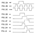
- the shift stages of the shift register 101 sequentially output the shift pulses Vs1 to Vsn having the same pulse width as the period of the horizontal clocks HCK and HCKX.
- These shift pulses Vs1 to Vsn are supplied to switches 102-1 to 102-n of the clock sampling switch group 102.
- each of the switches 102-1 to 102-n of the clock sampling switch group 102 are alternately connected to clock lines 104-1 and 104-2 receiving the horizontal clocks HCK and HCKX as input.
- the switches 102-1 to 102-n are turned on in sequence and sample the horizontal clocks HCKX and HCK.
- Each of these sampled pulses is supplied, as the sampling pulses Vh1 to Vhn, to switches 103-1 to 103-n of the sampling switch group 103.
- each of the switches 103-1 to 103-n of the sampling switch group 103 is connected to a video line 105 transmitting a video signal VOD.
- the switches 103-1 to 103-n turn on in sequence in response to the sampling pulses Vh1 to Vhn which are supplied in sequence as a result of being sampled by the switches 102-1 to 102-n of the clock sampling switch group 102, thereby sampling the video signal VDO, and supply it to signal lines 106-1 to 106-n of a pixel part (not illustrated).
- the horizontal driving circuit 100 using the clock driving method according to the above-described conventional example during the transmission process from when the horizontal clocks HCKX and HCK are sampled by the switches 102-1 to 102-n of the clock sampling switch group 102 until these are supplied as the sampling pulses Vh1 to Vhn to the switches 103-1 to 103-n of the sampling switch group 103, a delay occurs in the pulses due to wiring resistance, parasitic capacitance, etc.
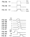
- the video signal VDO As shown in FIG. 5A, has a portion of a black level BLVL in a pulse state.
- the pulse width thereof is input as a waveform equal to the pulse width of a sampling pulse SMPL as shown in FIG. 5B.
- This pulse-state video signal VDO is ideally a rectangular wave, but the rising or falling edge of the pulse waveform becomes rounded (video signal VDO') as shown in FIG. 5C due to the wiring resistance, parasitic capacitance, etc. of the video line for transmitting the video signal VDO.
- BGLVL of FIGS. 5A and 5C indicate background gray levels.
- the black signal section (pulse section) of the video signal VDO overlaps the sampling pulse Vhk-1 of the (k-1)-th stage, the black signal is written also into the signal line of the (k-1)-th stage.
- a ghost GST occurs at the position of the (k-1)-th stage, that is, in front in a horizontal scanning direction HSCND (VSCND indicates a vertical scanning direction).
- S/H 0, the sampling pulse Vhk-1 of the (k-1)-th stage and the black signal section of the video signal VDO overlap each other, so a ghost GST occurs in front in the horizontal scanning direction HSCND.
- the video black signal overlaps the sampling pulse Vhk+1 of the (k+1)-th stage.
- the black signal is written into the signal line of the (k+1)-th stage when the sampling switch is turned on, then the line tries to return to the gray level.
- the potential of the signal line does not completely return to the gray level BGLVL by the amount indicated by NRTN in FIG. 9G.
- a ghost GST occurs at the position of the (k+1)-th stage, that is, behind in the horizontal scanning direction HSCND.
- a ghost occurs due to the overlap of the video signal VDO and the sampling pulse.
- the pulse waveform portion of the related video signal VDO overlaps the sampling pulse of the previous stage or subsequent stage, so it is impossible to obtain a larger ghost margin by that amount.
- a display device for obtaining shift pulses in sequence in synchronization with a first clock signal at the time of horizontal scanning with respect to a pixel part comprised by pixels arranged in a matrix and having a signal line arranged for each pixel string and for supplying a video signal to the signal line of said pixel part while sampling the video signal based on these shift pulses, wherein a second clock signal having the same period and having a smaller duty ratio than the first clock signal is generated, the second clock pulse is sampled based on the shift pulse and used as the sampling pulse, and the video signal is supplied to a signal line of the pixel part while sampling the video signal by this sampling pulse.
- each switch of the first switch group samples a second clock signal in sequence in response to a shift pulse which is output in sequence in synchronization with a first clock signal from the shift register.
- the second clock signal having a duty ratio smaller than that of the first clock signal is supplied, as a sampling signal, to the second switch group.
- each switch of the second switch group samples and holds the input video signal in sequence in response to these sampling signals and supplies the signal to the signal line of the pixel part.
- the duty ratio of the sampling signal is smaller than that of the first clock signal, perfectly non-overlapping sampling can be realized.
- FIG. 11 is a circuit diagram of an example of the configuration of an active-matrix type liquid crystal display device using the point-sequence driving method according to an embodiment of the present invention using for example liquid-crystal cells as pixel display elements (electro-optical elements).
- pixel display elements electronic-optical elements
- FIG. 11 a circuit diagram of an example of the configuration of an active-matrix type liquid crystal display device using the point-sequence driving method according to an embodiment of the present invention using for example liquid-crystal cells as pixel display elements (electro-optical elements).
- pixel display elements electro-optical elements
- each of the pixels (PXL) 11 of the 4 rows and 4 columns arranged in a matrix is comprised of a pixel transistor, that is, a thin-film transistor TFT, a liquid-crystal cell LC whose pixel electrode is connected to a drain electrode of this thin-film transistor TFT, and a holding capacitor Cs one electrode of which is connected to the drain electrode of the thin-film transistor TFT.
- Signal lines 12-1 to 12-4 are laid for the columns of these pixels 11 along the pixel array direction, while gate lines 13-1 to 13-4 are laid for the rows along the pixel array direction.
- source electrodes (or the drain electrodes) of the thin-film transistors TFT are connected to the corresponding signal lines 12-1 to 12-4.
- Gate electrodes of the thin-film transistors TFT are connected to the corresponding gate lines 13-1 to 13-4.
- the counter electrodes of the liquid-crystal cells LC and the other electrodes of the holding capacitors Cs are connected to a Cs line 14 common for the pixels.
- a predetermined DC voltage is supplied as a common voltage Vcom to this Cs line 14.
- a pixel part (PXLP) 15 is formed in which pixels 11 are arranged in a matrix, signal lines 12-1 to 12-4 are laid for the columns of these pixels 11, and gate lines 13-1 to 13-4 are laid for the rows.
- one end of each of the gate lines 13-1 to 13-4 is connected to an output end of each row of a vertical driving circuit (VDRV) 16 disposed, for example, to the left of the pixel part 15.
- VDRV vertical driving circuit
- the vertical driving circuit 16 performs processing for scanning in the vertical direction (row direction) at each field period so as to select the pixels 11 connected to the gate lines 13-1 to 13-4 in sequence in row units. Namely, when a scanning pulse Vg1 is supplied from the vertical driving circuit 16 to the gate line 13-1, the pixels of the columns of the first row are selected, while when a scanning pulse Vg2 is supplied to the gate line 13-2, the pixels of the columns of the second row are selected.
- scanning pulses Vg3 and Vg4 are supplied in sequence to the gate lines 13-3 and 13-4.
- a horizontal driving circuit (HDRV) 17 is disposed above for example the pixel part 15, a horizontal driving circuit (HDRV) 17 is disposed. Also, a clock generating circuit (CLKGEN: timing generator) 18 for supplying various clock signals to the vertical driving circuit 16 and the horizontal driving circuit 17 is provided.
- This clock generating circuit 18 generates a vertical start pulse VST for instructing the start of vertical scanning, opposite phase vertical clocks VCK and VCKX serving as a vertical scanning reference, a vertical start pulse VST for instructing the start of horizontal scanning, and opposite phase horizontal clocks HCK and HCKX serving as a horizontal scanning reference.
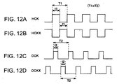
- the clock generating circuit 18, furthermore, as shown in the timing charts of FIGS. 12A to 12D, also generates opposite phase clocks DCK and DCKX having the same period (T1 T2) as that of the horizontal clocks HCK and HCKX and having a smaller duty ratio.
- the duty ratio is a ratio of the pulse width t to the pulse repetition period T in the pulse waveform.
- the duty ratio (t1/T1) of the horizontal clocks HCK and HCKX is 50%
- the duty ratio (t2/T2) of the clocks DCK and DCKX is set to be smaller than this percentage, that is, the pulse width t2 of the clocks DCK and DCKX is set to be smaller than the pulse width t1 of the horizontal clocks HCK and HCKX.
- the horizontal driving circuit 17 is for sampling the input video signal VDO in sequence at intervals of 1H (H is the horizontal scanning period) and for performing a writing process on each pixel 11 selected in row units by the vertical driving circuit 16.
- the present example is configured employing a clock driving method and having a shift register 21, a clock sampling switch group 22, and a sampling switch group 23.
- the shift register 21 is comprised by four shift stages (S/R stages) 21-1 to 21-4 corresponding to the pixel strings of the pixel part 15 (in the present example, four columns).
- the shift register 21 performs a shift operation in synchronization with the opposite phase horizontal clocks HCK and HCKX.
- the clock sampling switch group 22 is formed of four switches 22-1 to 22-4 corresponding to the pixel strings of the pixel part 15. Ends of each of these switches 22-1 to 22-4 are alternately connected to the clock lines 24-1 and 24-2 which transmit the clocks DCKX and DCK from the clock generating circuit 18. Namely, one end of each of the switches 22-1 and 22-3 is connected to the clock line 24-1, and one end of each of the switches 22-2 and 22-4 is connected to the clock line 24-2.
- the shift pulses Vs1 to Vs4 which are output in sequence from the shift stages 21-1 to 21-4 of the shift register 21 are supplied to the switches 22-1 to 22-4 of the clock sampling switch group 22.
- the switches 22-1 to 22-4 are turned on in sequence in response to these shift pulses Vs1 to Vs4, thereby alternately sampling the opposite phase clocks DCKX and DCK.
- the sampling switch group 23 is formed of four switches 23-1 to 23-4 corresponding to the pixel strings of the pixel part 15. One end of each of these switches 23-1 to 23-4 is connected to a video line 25 receiving a video signal VDO as input.
- the switches 23-1 to 23-4 of the sampling switch group 23 are turned on in sequence in response to these sampling pulses Vh1 to Vh4, thereby sequentially sampling the video signal VDO which is input through the video line 25, and supply the signal to the signal lines 12-1 to 12-4 of the pixel part 15.
- the opposite phase clocks DCKX and DCK are sampled alternately in synchronization with the sampling pulses Vh1 to Vh4 and these clocks DCKX and DCK are used directly as the sampling pulses Vh1 to Vh4, making it possible to suppress variations of the sampling pulses Vh1 to Vh4. As a result, it becomes possible to eliminate ghosts caused by variations of the sampling pulses Vh1 to Vh4.
- the horizontal driving circuit 17 rather than sampling the horizontal clocks HCKX and HCK which serve as a reference for the shift operation of the shift register 21 and using them as the sampling pulses Vh1 to Vh4 as in the related art, the clocks DCKX and DCK having the same period as that of the horizontal clocks HCKX and HCK and having a smaller duty ratio are separately generated. These clocks DCKX and DCK are sampled and used as the sampling pulses Vh1 to Vh4. As a consequence, the operation and effect such as those described below are obtained.
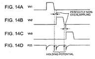
- each of the sampled clocks DCKX and DCK has a perfectly non-overlapping waveform with respect to the previous and subsequent pulses. Note that, FIG. 14D shows a potential P25 of the video line 25.
- the sampling switch group 23 when a particular k-th stage is considered, the sampling of the video signal VDO by the sampling switch of the k-th stage can always be completed before the sampling switch of the (k+1)-th stage is turned on.
- S/H 0 to 5
- SMPL perfectly non-overlapping sampling pulses
- the video black signal overlaps the sampling pulse Vhk+1 of the (k+1)-th stage.
- the black signal is written into the signal line of the (k+1)-th stage when the sampling switch is turned on, then the line tries to return to the gray level.
- the potential!of the signal line does not completely return to the gray level by exactly the amount indicated by NRTN in FIG. 17G. Accordingly, a ghost occurs behind in the horizontal scanning direction.
- the present invention is not limited to application to an LCD device and can be applied to active-matrix type liquid crystal display devices in general using a point-sequence driving method employing a clock driving method for horizontal driving circuits, for example an active-matrix-type EL display device using an electroluminescence (EL) element as the display element of each pixel.
- EL electroluminescence
- Examples of the point-sequence driving method include, in addition to the well known 1H inversion driving method and dot inversion driving method, the so-called dot line inversion driving method in which video signals having opposite polarities are written simultaneously into the pixels of two rows separated by odd-numbered rows among adjacent pixel strings, for example, the pixels of two rows, i.e., an upper row and a lower row, so that the polarities of the pixels become the same in the right and left adjacent pixels and become opposite polarities in the upper and lower pixels in the pixel array after the video signals are written.
- the so-called dot line inversion driving method in which video signals having opposite polarities are written simultaneously into the pixels of two rows separated by odd-numbered rows among adjacent pixel strings, for example, the pixels of two rows, i.e., an upper row and a lower row, so that the polarities of the pixels become the same in the right and left adjacent pixels and become opposite polarities in the upper and lower pixels in the pixel array after the video signals are written.
- the active-matrix-type liquid crystal display device using the point-sequence driving method according to the embodiment explained above can be used as a display panel of a projection type liquid crystal display device (liquid-crystal projector), that is, an LCD (liquid-crystal display) panel.
- liquid-crystal projector liquid-crystal projector
- LCD liquid-crystal display
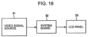
- FIG. 18 is a block diagram of the system configuration of the projection type liquid crystal display device.
- the projection type liquid crystal display device according to the present example is comprised of a video signal source 31, system board 32, and LCD panel 33.
- the system board 32 performs signal processing such as adjustment of the above mentioned sampling and holding position with respect to a video signal which is output from the video signal source 31.
- the system board 32 also mounts the clock generating circuit (timing generator) 18 of FIG. 11.
- the LCD panel 33 use is made of an active-matrix type liquid crystal display device using the point-sequence driving method according to the above mentioned embodiment. Also, in the case of color, LCD panels 33 are provided corresponding to R (red), G (green), and B (blue).
- FIG. 19 is a schematic view of the configuration showing an example of the configuration of the optical system of the projection type color liquid crystal display device.
- a specific color component in white light emitted from a light source 41 for example, a B (blue) component having the shortest wavelength, passes through a first beam splitter 42, while the remaining color components are reflected.
- the B component passed through the first beam splitter 42 is changed in its optical path at a mirror 43 and emitted to an LCD panel 45B through a lens 44.
- the for example G (green) component is reflected at a second beam splitter 46, while the R (red) component passes through it.
- the G component reflected at the second beam splitter 46 is emitted to a G LCD panel 45G through a lens 47.
- the R component passed through the second beam splitter 46 is changed in its optical path at mirrors 48 and 49 and emitted to an R LCD panel 45R through a lens 50.
- Each of the LCD panels 45R, 45G, and 45B is configured by a first base plate having a plurality of pixels arranged in a matrix, a second base plate oppositely arranged with a predetermined interval with respect to this first base plate, a liquid-crystal layer held between these base plates, and filter layers corresponding to the colors.
- the R, G, and B light components passing through these LCD panels 45R, 45G, and 45B are optically combined by a cross prism 51. Then, the composite light emitted from this cross prism 51 is projected to a screen 53 by a projection prism 52.
- the projection type liquid crystal display device having the above-described configuration, by using active-matrix type liquid crystal display devices using the point-sequence driving method according to the above mentioned embodiment as the LCD panels 45R, 45G, and 45B, perfectly non-overlapping sampling is realized in the horizontal driving system in the related liquid crystal display devices, whereby the occurrence of streaks caused by overlapping sampling can be suppressed, and the ghost margin can be raised, so a higher quality image display can be realized.
- projection type liquid crystal display devices include a rear type and a front type.
- a rear type projection type liquid crystal display device has been used as a projection TV for moving pictures
- a front type projection type liquid crystal display device has been used as a data projector
- the active-matrix type liquid crystal display device using the point-sequence driving method according to the above mentioned embodiment can be applied to both types.
- an explanation was made of the case where the present invention was applied to a color projection type liquid crystal display device as an example, but the present invention can be similarly applied also to a monochrome projection type liquid crystal display device.
- a second clock signal having the same period and having a smaller duty ratio than a first clock signal serving as a horizontal scanning reference is generated, this second clock signal is sampled, and the video signal is sampled using this as the sampling pulse, whereby perfectly non-overlapping sampling can be realized, so the occurrence of streaks caused by overlapping sampling can be suppressed, and the ghost margin can be raised.
Landscapes
- Engineering & Computer Science (AREA)
- Chemical & Material Sciences (AREA)
- Crystallography & Structural Chemistry (AREA)
- Physics & Mathematics (AREA)
- Computer Hardware Design (AREA)
- General Physics & Mathematics (AREA)
- Theoretical Computer Science (AREA)
- Liquid Crystal Display Device Control (AREA)
- Control Of Indicators Other Than Cathode Ray Tubes (AREA)
- Liquid Crystal (AREA)
Abstract
Description
Claims (6)
- A display device, comprising:a pixel part comprised of pixels arranged in a matrix and having a signal line arranged for each pixel string,a clock generating means for generating a first clock signal serving as a reference for horizontal scanning and generating a second clock signal having the same period and having a smaller duty ratio than the first clock signal,a shift register for performing a shift operation in synchronization with said first clock signal and outputting a shift pulse in sequence from the shift stages,a first switch group for sampling said second clock signal in response to a shift pulse output in sequence from said shift register, anda second switch group for sampling an input video signal in sequence in response to said second clock signal sampled by the switches of the first switch group and supplying the same to the signal lines of the pixel part.
- A display device as set forth in claim 1, wherein a display element of each pixel of said pixel part is a liquid-crystal cell.
- A method of driving a display device for obtaining shift pulses in sequence in synchronization with a first clock signal at the time of horizontal scanning with respect to a pixel part comprised by pixels arranged in a matrix and having a signal line arranged for each pixel string and for supplying a video signal to the signal line of said pixel part while sampling the video signal based on these shift pulses, comprising:generating a second clock signal having the same period and having a smaller duty ratio than the first clock signal,sampling the second clock pulse based on the shift pulse and using it as the sampling pulse, andsupplying the video signal to a signal line of the pixel part while sampling the video signal by this sampling pulse.
- A method of driving a display device as set forth in claim 3, wherein a display element of each pixel of said pixel part is a liquid-crystal cell.
- A projection type display device, comprising:a clock generating means for generating a first clock signal serving as a reference for horizontal scanning and generating a second clock signal having the same period and having a smaller duty ratio than the first clock signal,a display panel having a pixel part comprised by pixels arranged in a matrix and having a signal line arranged for each pixel string and a horizontal driving system for sampling said second clock signal based on a shift pulse obtained in sequence in synchronization with said first clock signal and sampling an input video signal in sequence in response to said sampled second clock signal and supplying the same to the signal lines of the pixel part,an emitting means for emitting light to said display panel, anda projecting means for projecting light passing through the display panel to a screen.
- A projection type display device as set forth in claim 5, wherein a display element of each pixel of said pixel part is a liquid-crystal cell.
Applications Claiming Priority (3)
| Application Number | Priority Date | Filing Date | Title |
|---|---|---|---|
| JP2000177927 | 2000-06-14 | ||
| JP2000177927 | 2000-06-14 | ||
| PCT/JP2001/005063 WO2001097205A1 (en) | 2000-06-14 | 2001-06-14 | Display device and its driving method, and projection-type display device |
Publications (2)
| Publication Number | Publication Date |
|---|---|
| EP1300825A1 true EP1300825A1 (en) | 2003-04-09 |
| EP1300825A4 EP1300825A4 (en) | 2005-11-09 |
Family
ID=18679447
Family Applications (1)
| Application Number | Title | Priority Date | Filing Date |
|---|---|---|---|
| EP01938660A Withdrawn EP1300825A4 (en) | 2000-06-14 | 2001-06-14 | DISPLAY DEVICE AND METHOD FOR CONTROLLING THE SAME, AND PROJECTION DISPLAY DEVICE |
Country Status (6)
| Country | Link |
|---|---|
| US (1) | US20020149558A1 (en) |
| EP (1) | EP1300825A4 (en) |
| KR (1) | KR20020005421A (en) |
| NO (1) | NO20020730L (en) |
| TW (1) | TW507190B (en) |
| WO (1) | WO2001097205A1 (en) |
Cited By (1)
| Publication number | Priority date | Publication date | Assignee | Title |
|---|---|---|---|---|
| CN112614469A (en) * | 2020-12-24 | 2021-04-06 | 北京集创北方科技股份有限公司 | Electronic device, driving apparatus, power supply, and electronic apparatus |
Families Citing this family (12)
| Publication number | Priority date | Publication date | Assignee | Title |
|---|---|---|---|---|
| TW562972B (en) * | 2001-02-07 | 2003-11-21 | Toshiba Corp | Driving method for flat-panel display device |
| JP3633528B2 (en) * | 2001-08-24 | 2005-03-30 | ソニー株式会社 | Display device |
| CN100359552C (en) * | 2001-10-17 | 2008-01-02 | 索尼株式会社 | display screen |
| JP3890948B2 (en) | 2001-10-17 | 2007-03-07 | ソニー株式会社 | Display device |
| JP3968499B2 (en) * | 2001-10-17 | 2007-08-29 | ソニー株式会社 | Display device |
| JP3755484B2 (en) * | 2002-05-21 | 2006-03-15 | ソニー株式会社 | Display device |
| JP2004309822A (en) * | 2003-04-08 | 2004-11-04 | Sony Corp | Display device |
| JP3870933B2 (en) * | 2003-06-24 | 2007-01-24 | ソニー株式会社 | Display device and driving method thereof |
| JP4089546B2 (en) | 2003-08-04 | 2008-05-28 | ソニー株式会社 | Display device and driving method thereof |
| JP2005148557A (en) * | 2003-11-18 | 2005-06-09 | Sony Corp | Display device and projection display device |
| JP3872085B2 (en) * | 2005-06-14 | 2007-01-24 | シャープ株式会社 | Display device drive circuit, pulse generation method, and display device |
| KR101941447B1 (en) * | 2012-04-18 | 2019-01-23 | 엘지디스플레이 주식회사 | Flat display device |
Family Cites Families (6)
| Publication number | Priority date | Publication date | Assignee | Title |
|---|---|---|---|---|
| JPH10143115A (en) * | 1996-11-11 | 1998-05-29 | Sharp Corp | Active matrix type image display |
| WO1999023530A1 (en) * | 1997-10-31 | 1999-05-14 | Seiko Epson Corporation | Electro-optical device and electronic apparatus |
| US6377235B1 (en) * | 1997-11-28 | 2002-04-23 | Seiko Epson Corporation | Drive circuit for electro-optic apparatus, method of driving the electro-optic apparatus, electro-optic apparatus, and electronic apparatus |
| JP3846057B2 (en) * | 1998-09-03 | 2006-11-15 | セイコーエプソン株式会社 | Electro-optical device drive circuit, electro-optical device, and electronic apparatus |
| JP2000310963A (en) * | 1999-02-23 | 2000-11-07 | Seiko Epson Corp | Driving circuit for electro-optical device, electro-optical device, and electronic apparatus |
| JP2000310964A (en) * | 1999-02-23 | 2000-11-07 | Seiko Epson Corp | Driving circuit for electro-optical device, electro-optical device, and electronic apparatus |
-
2001
- 2001-06-13 TW TW090114308A patent/TW507190B/en active
- 2001-06-13 KR KR1020010033279A patent/KR20020005421A/en not_active Withdrawn
- 2001-06-14 WO PCT/JP2001/005063 patent/WO2001097205A1/en not_active Ceased
- 2001-06-14 EP EP01938660A patent/EP1300825A4/en not_active Withdrawn
- 2001-06-14 US US10/049,520 patent/US20020149558A1/en not_active Abandoned
-
2002
- 2002-02-13 NO NO20020730A patent/NO20020730L/en not_active Application Discontinuation
Cited By (2)
| Publication number | Priority date | Publication date | Assignee | Title |
|---|---|---|---|---|
| CN112614469A (en) * | 2020-12-24 | 2021-04-06 | 北京集创北方科技股份有限公司 | Electronic device, driving apparatus, power supply, and electronic apparatus |
| CN112614469B (en) * | 2020-12-24 | 2022-05-20 | 北京集创北方科技股份有限公司 | Electronic device, driving apparatus, power supply, and electronic apparatus |
Also Published As
| Publication number | Publication date |
|---|---|
| US20020149558A1 (en) | 2002-10-17 |
| EP1300825A4 (en) | 2005-11-09 |
| WO2001097205A1 (en) | 2001-12-20 |
| NO20020730D0 (en) | 2002-02-13 |
| KR20020005421A (en) | 2002-01-17 |
| NO20020730L (en) | 2002-04-08 |
| TW507190B (en) | 2002-10-21 |
Similar Documents
| Publication | Publication Date | Title |
|---|---|---|
| US5648793A (en) | Driving system for active matrix liquid crystal display | |
| KR101620104B1 (en) | Apparatus and method for driving electro-optical device, the electro-optical device, and an electronic apparatus | |
| KR101026809B1 (en) | Impulsive driving liquid crystal display device and driving method thereof | |
| EP1300825A1 (en) | Display device and its driving method, and projection-type display device | |
| US20080180462A1 (en) | Liquid crystal display device and method of driving liquid crystal display device | |
| KR100893966B1 (en) | Display appratus | |
| US7151538B2 (en) | Display device and projection type display device | |
| KR100686502B1 (en) | Electro-optical device and its driving method, driving circuit and electronic device of electro-optical device | |
| KR101051605B1 (en) | Display device and driving method thereof | |
| US9564095B2 (en) | Liquid crystal display device and method for driving the liquid crystal display device whereby shadowing can be prevented | |
| KR100954012B1 (en) | Display device | |
| US20070285383A1 (en) | Electro-optical device, method for driving electro-optical device, and electronic apparatus | |
| WO2018221477A1 (en) | Liquid crystal display device | |
| KR20050062158A (en) | Impulsive driving liquid crystal display and driving method thereof | |
| JP3900256B2 (en) | Liquid crystal drive device and liquid crystal display device | |
| KR20110076086A (en) | Silicone liquid crystal display | |
| JP2002072987A (en) | Display device, driving method thereof, and projection display device | |
| HK1055636A1 (en) | Display device and its driving method, and projection-type display device | |
| JP2003330431A (en) | Liquid crystal display | |
| KR20040087933A (en) | Display device | |
| JPH0926583A (en) | Liquid crystal panel and projection type image display device using the same | |
| JP3788435B2 (en) | Display device and projection display device | |
| JP4552595B2 (en) | Electro-optical device, image signal processing method thereof, and electronic apparatus | |
| JP3852418B2 (en) | Display device and projection display device | |
| JP3852417B2 (en) | Display device and projection display device |
Legal Events
| Date | Code | Title | Description |
|---|---|---|---|
| PUAI | Public reference made under article 153(3) epc to a published international application that has entered the european phase |
Free format text: ORIGINAL CODE: 0009012 |
|
| 17P | Request for examination filed |
Effective date: 20020215 |
|
| AK | Designated contracting states |
Kind code of ref document: A1 Designated state(s): AT BE CH CY DE DK ES FI FR GB GR IE IT LI LU MC NL PT SE TR Designated state(s): AT BE CH CY DE DK ES FI FR GB GR IE IT LI LU MC NL PT SE TR |
|
| AX | Request for extension of the european patent |
Extension state: AL LT LV MK RO SI |
|
| RBV | Designated contracting states (corrected) |
Designated state(s): BE GB NL |
|
| REG | Reference to a national code |
Ref country code: DE Ref legal event code: 8566 |
|
| A4 | Supplementary search report drawn up and despatched |
Effective date: 20050928 |
|
| STAA | Information on the status of an ep patent application or granted ep patent |
Free format text: STATUS: THE APPLICATION IS DEEMED TO BE WITHDRAWN |
|
| 18D | Application deemed to be withdrawn |
Effective date: 20060503 |
|
| REG | Reference to a national code |
Ref country code: HK Ref legal event code: WD Ref document number: 1055636 Country of ref document: HK |