EP1298967A2 - Electronic card - Google Patents
Electronic card Download PDFInfo
- Publication number
- EP1298967A2 EP1298967A2 EP02021557A EP02021557A EP1298967A2 EP 1298967 A2 EP1298967 A2 EP 1298967A2 EP 02021557 A EP02021557 A EP 02021557A EP 02021557 A EP02021557 A EP 02021557A EP 1298967 A2 EP1298967 A2 EP 1298967A2
- Authority
- EP
- European Patent Office
- Prior art keywords
- patterns
- circuit board
- circuit
- electronic card
- charge prevention
- Prior art date
- Legal status (The legal status is an assumption and is not a legal conclusion. Google has not performed a legal analysis and makes no representation as to the accuracy of the status listed.)
- Granted
Links
Images



Classifications
-
- G—PHYSICS
- G06—COMPUTING OR CALCULATING; COUNTING
- G06K—GRAPHICAL DATA READING; PRESENTATION OF DATA; RECORD CARRIERS; HANDLING RECORD CARRIERS
- G06K19/00—Record carriers for use with machines and with at least a part designed to carry digital markings
- G06K19/06—Record carriers for use with machines and with at least a part designed to carry digital markings characterised by the kind of the digital marking, e.g. shape, nature, code
- G06K19/067—Record carriers with conductive marks, printed circuits or semiconductor circuit elements, e.g. credit or identity cards also with resonating or responding marks without active components
- G06K19/07—Record carriers with conductive marks, printed circuits or semiconductor circuit elements, e.g. credit or identity cards also with resonating or responding marks without active components with integrated circuit chips
- G06K19/077—Constructional details, e.g. mounting of circuits in the carrier
-
- G—PHYSICS
- G06—COMPUTING OR CALCULATING; COUNTING
- G06K—GRAPHICAL DATA READING; PRESENTATION OF DATA; RECORD CARRIERS; HANDLING RECORD CARRIERS
- G06K19/00—Record carriers for use with machines and with at least a part designed to carry digital markings
- G06K19/06—Record carriers for use with machines and with at least a part designed to carry digital markings characterised by the kind of the digital marking, e.g. shape, nature, code
- G06K19/067—Record carriers with conductive marks, printed circuits or semiconductor circuit elements, e.g. credit or identity cards also with resonating or responding marks without active components
- G06K19/07—Record carriers with conductive marks, printed circuits or semiconductor circuit elements, e.g. credit or identity cards also with resonating or responding marks without active components with integrated circuit chips
- G06K19/077—Constructional details, e.g. mounting of circuits in the carrier
- G06K19/0772—Physical layout of the record carrier
- G06K19/07735—Physical layout of the record carrier the record carrier comprising means for protecting against electrostatic discharge
-
- H—ELECTRICITY
- H05—ELECTRIC TECHNIQUES NOT OTHERWISE PROVIDED FOR
- H05K—PRINTED CIRCUITS; CASINGS OR CONSTRUCTIONAL DETAILS OF ELECTRIC APPARATUS; MANUFACTURE OF ASSEMBLAGES OF ELECTRICAL COMPONENTS
- H05K1/00—Printed circuits
- H05K1/02—Details
- H05K1/0213—Electrical arrangements not otherwise provided for
- H05K1/0254—High voltage adaptations; Electrical insulation details; Overvoltage or electrostatic discharge protection ; Arrangements for regulating voltages or for using plural voltages
- H05K1/0257—Overvoltage protection
- H05K1/0259—Electrostatic discharge [ESD] protection
-
- H—ELECTRICITY
- H05—ELECTRIC TECHNIQUES NOT OTHERWISE PROVIDED FOR
- H05K—PRINTED CIRCUITS; CASINGS OR CONSTRUCTIONAL DETAILS OF ELECTRIC APPARATUS; MANUFACTURE OF ASSEMBLAGES OF ELECTRICAL COMPONENTS
- H05K3/00—Apparatus or processes for manufacturing printed circuits
- H05K3/22—Secondary treatment of printed circuits
- H05K3/24—Reinforcing of the conductive pattern
- H05K3/241—Reinforcing of the conductive pattern characterised by the electroplating method; means therefor, e.g. baths or apparatus
- H05K3/242—Reinforcing of the conductive pattern characterised by the electroplating method; means therefor, e.g. baths or apparatus characterised by using temporary conductors on the printed circuit for electrically connecting areas which are to be electroplated
-
- H—ELECTRICITY
- H05—ELECTRIC TECHNIQUES NOT OTHERWISE PROVIDED FOR
- H05K—PRINTED CIRCUITS; CASINGS OR CONSTRUCTIONAL DETAILS OF ELECTRIC APPARATUS; MANUFACTURE OF ASSEMBLAGES OF ELECTRICAL COMPONENTS
- H05K2201/00—Indexing scheme relating to printed circuits covered by H05K1/00
- H05K2201/03—Conductive materials
- H05K2201/0332—Structure of the conductor
- H05K2201/0335—Layered conductors or foils
- H05K2201/0352—Differences between the conductors of different layers of a multilayer
-
- H—ELECTRICITY
- H05—ELECTRIC TECHNIQUES NOT OTHERWISE PROVIDED FOR
- H05K—PRINTED CIRCUITS; CASINGS OR CONSTRUCTIONAL DETAILS OF ELECTRIC APPARATUS; MANUFACTURE OF ASSEMBLAGES OF ELECTRICAL COMPONENTS
- H05K2201/00—Indexing scheme relating to printed circuits covered by H05K1/00
- H05K2201/09—Shape and layout
- H05K2201/09209—Shape and layout details of conductors
- H05K2201/09654—Shape and layout details of conductors covering at least two types of conductors provided for in H05K2201/09218 - H05K2201/095
- H05K2201/09709—Staggered pads, lands or terminals; Parallel conductors in different planes
-
- H—ELECTRICITY
- H05—ELECTRIC TECHNIQUES NOT OTHERWISE PROVIDED FOR
- H05K—PRINTED CIRCUITS; CASINGS OR CONSTRUCTIONAL DETAILS OF ELECTRIC APPARATUS; MANUFACTURE OF ASSEMBLAGES OF ELECTRICAL COMPONENTS
- H05K2201/00—Indexing scheme relating to printed circuits covered by H05K1/00
- H05K2201/09—Shape and layout
- H05K2201/09209—Shape and layout details of conductors
- H05K2201/09654—Shape and layout details of conductors covering at least two types of conductors provided for in H05K2201/09218 - H05K2201/095
- H05K2201/09781—Dummy conductors, i.e. not used for normal transport of current; Dummy electrodes of components
-
- H—ELECTRICITY
- H05—ELECTRIC TECHNIQUES NOT OTHERWISE PROVIDED FOR
- H05K—PRINTED CIRCUITS; CASINGS OR CONSTRUCTIONAL DETAILS OF ELECTRIC APPARATUS; MANUFACTURE OF ASSEMBLAGES OF ELECTRICAL COMPONENTS
- H05K3/00—Apparatus or processes for manufacturing printed circuits
- H05K3/22—Secondary treatment of printed circuits
- H05K3/28—Applying non-metallic protective coatings
- H05K3/281—Applying non-metallic protective coatings by means of a preformed insulating foil
Definitions
- the present invention relates to electronic cards formed of a double-sided printed circuit board.
- Electronic cards such as an SD (Secure Digital) card which is formed of a non-volatile semiconductor memory device and which constitutes, for example, a small-sized memory card is inserted into and removed from an electronic equipment by gripping it.
- SD Secure Digital
- card surfaces may be formed by covering only a component mounted surface formed on one surface of a printed circuit board, with a card case, and coating a wiring pattern portion on the other surface with a protective film composed of, for example, ultraviolet hardened resin. More effective electrostatic prevention measures are required for such small-sized very thin electronic cards.
- electrolytic plating patterns required for gold plating or the like in a desired circuit pattern are continuously disposed over a plurality of circuit boards before the individual circuit boards are blanked. After the individual circuit boards have been obtained, the patterns remain at the edges of the circuit boards. These electrolytic plating patterns remain connected to circuit patterns forming internal signal paths. Thus, when a discharge current induced by static electricity flows into the patterns formed at the edges of the circuit board, it may destroy the internal circuit or data or result in other problems. Thus, effective electrostatic measures have been required particularly for the patterns formed at that edge of the circuit board which is located closer to the grip portion.
- An embodiment of the present invention is directed to an electronic card that substantially obviates one or more of the problems due to limitations and disadvantages of the related art.
- an electronic card comprises:
- an SD card will be described as an electronic card to which the present invention is applied.
- FIGS. 1A to 4 show a first embodiment in which the present invention is applied to an SD card.
- a circuit component mounted surface 20B (hereinafter referred to as a "front surface") of a very thin double-sided printed circuit board (hereinafter simply referred to as a "circuit board”) is entirely covered with a card case 10 to protect internal circuit components, as shown in FIG. 1B.
- the card case 10 is composed of a flat and rectangular synthetic resin material and has a grip portion 11 formed at one end thereof and formed of a recessed groove, as shown in FIG. 1A.
- the circuit board 20 has a plurality of contact terminals TP, TP, ...
- a back surface disposed on the opposite surface (hereinafter referred to as a "back surface") of the circuit board 20 at one side thereof located opposite the grip portion 11 as shown in FIG. 1C.
- the contact terminals TP, TP, ... are exposed, with the rest of the back surface 20A coated flat with a protective film composed of, for example, ultraviolet hardened resin or the like.
- This coating layer 30 forms a card surface.
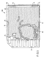
- FIG. 2 shows the details of the front surface 20B of the circuit board 20.
- Circuit component mounting patterns and circuit patterns forming signal paths are disposed on the front surface 20B.
- a circuit component 21 is soldered onto the circuit component mounting patterns by reflow.
- a plurality of electrolytic plating patterns CP, CP, ... connected to the circuit patterns forming the signal paths are disposed so as to extend from end surfaces of the circuit board.
- FIG. 3 shows the details of the back surface 20A of the circuit board 20.
- the back surface 20A is provided with a ground pattern GP forming a ground potential on the circuit.
- a plurality of charge prevention patterns GL, GL, ... connected to the ground pattern GP and corresponding to the electrolytic plating patterns CP, CP, ... are disposed so as to extend from edges of the circuit board 20.
- the charge prevention patterns GL, GL, ... may be connected to a power supply pattern.
- the charge prevention patterns GL, GL, ... provided on the back surface 20A and the electrolytic plating patterns CP, CP, ... disposed on the front surface 20B are disposed in a zigzag fashion (alternately) at predetermined intervals, as shown in FIG. 4, which is a sectional view of an end surface of the circuit board 20.
- the thickness Da of the coating layer 30 is smaller than the thickness Db of the card case 10.
- the charge prevention patterns GL, GL, ... and the electrolytic plating patterns CP, CP, ... are disposed in a zigzag pattern. Further, each of the electrolytic plating patterns CP, CP, ... extends along the charge prevention patterns GL, GL, ... so as to be sandwiched therebetween. Furthermore, the thickness Da of the coating layer 30 is smaller than the thickness Db of the card case 10. Consequently, when a user grips the grip portion 11, formed in the card case 10, shown in FIG. 1A, to insert or remove the electronic card into or from a computer, etc., a discharge current induced by static electricity flows into the ground pattern GP via the charge prevention patterns GL, GL, ..., which are closest to the ground pattern GP. This avoids the disadvantage that a discharge current induced by static electricity flows into an internal circuit via the electrolytic plating patterns CP, CP, ....
- this embodiment provides an electronic card formed of a double-sided printed circuit board and which has a simple and inexpensive configuration and for which more effective electrostatic measures are taken.
- effective electrostatic measures can be taken for the patterns formed at that edge of the circuit board which is located closer to the gripped portion.
- this embodiment provides an electronic card comprising a double-sided printed circuit board in which a surface thereof on which components are mounted is covered with a cover member, while the other surface thereof is coated with a protective film except for external connection terminals, wherein charge prevention circuit patterns connected to a ground pattern or a power supply pattern are provided on the other surface of the circuit board.
- this embodiment provides an electronic card formed of a double-sided printed circuit board with a grip portion, the electronic card comprising signal patterns provided on one surface of the circuit board, located under the grip portion, charge prevention patterns, provided on the other surface of the circuit board located under the grip portion, a cover member covering one surface of the circuit board, and a coating layer coating the circuit patterns disposed on the other surface of the circuit board, wherein the thickness of the coating layer is smaller than the thickness of the cover member.
- this embodiment provides an electronic card formed of a double-sided circuit board, wherein with respect to circuit patterns provided on one surface of the circuit board and a plurality of electrolytic plating circuit patterns connected to the above circuit patterns and disposed so as to contact with edges of the circuit board, a plurality of charge prevention circuit patterns are disposed on the other surface of the circuit board so as to contact with edges thereof, the charge prevention circuit patterns being extended from a ground pattern or a power supply pattern along the electrolytic plating circuit patterns so as to sandwich each of'the electrolytic plating circuit patterns therebetween.
- this embodiment provides an electronic card formed of a double-sided circuit board, one surface of which has circuit patterns forming signal paths, and electrolytic plating circuit patterns connected to the circuit patterns, disposed so as to contact the edges of the circuit board.
- the other surface has a ground pattern or a power supply pattern and charge prevention circuit patterns disposed to extend from the ground or power supply pattern along the electrolytic plating circuit patterns and contact the edges of the circuit board.
- a protective cover member covers one surface of the circuit board, and a protective film covers circuit patterns provided on at least a part of the other surface of the circuit board. The thickness of the protective film is smaller than the thickness of the protective cover.
- this embodiment provides an electronic card formed of a double-sided circuit board, and the electronic card comprises signal patterns disposed on one surface of the circuit board at the grip portion; charge prevention patterns disposed on the other surface of the circuit board at the grip portion; a protective cover covering one surface of the circuit board; and a protective film covering circuit patterns provided on at least a part of the other surface of the circuit board.
- the thickness of the protective film is smaller than the thickness of the protective cover.
- the present invention is not limited to the above described embodiment.
- the charge prevention patterns GL, GL, ... are connected to the ground pattern to allow a discharge current induced by static electricity to flow to the ground (GND).
- the present invention is not limited to this connection, and, for example, the charge prevention patterns GL, GL, ... may be connected to another power supply line with a low impedance, for example, a Vcc line (terminal) through which power is supplied to the interior of the card.
- Vcc power supply source
- a discharge current induced by static electricity can be converged and discharged on a low-impedance circuit of the power supply source. Consequently, stable circuit operations can be maintained without affecting the operation driving voltage or signal level of the internal circuit.
- charge prevention measures are taken for the charge prevention patterns CP, CP, ... disposed up to the edges of the circuit board and connected to the patterns forming the signal paths for the internal circuit.
- the circuit patterns forming the signal paths may be protected from problems attributed to a discharge current induced by static electricity by disposing similar charge prevention patterns GL, GL, ... for the circuit patterns disposed on the other surface 20B of the circuit board 20, which is located under the grip portion 11, the circuit patterns forming the signal paths.
Landscapes
- Engineering & Computer Science (AREA)
- Microelectronics & Electronic Packaging (AREA)
- Computer Hardware Design (AREA)
- Physics & Mathematics (AREA)
- General Physics & Mathematics (AREA)
- Theoretical Computer Science (AREA)
- Manufacturing & Machinery (AREA)
- Credit Cards Or The Like (AREA)
- Structure Of Printed Boards (AREA)
- Electroplating Methods And Accessories (AREA)
Abstract
Description
Claims (12)
- An electronic card comprising:a printed circuit board (20) which has components mounted on one surface thereof;a cover member (10) which covers the one surface of the printed circuit board; andexternal connection terminals (TP) provided on the other surface of the printed circuit board,
characterized by further comprising:charge prevention circuit patters (GL) provided on the other surface of the printed circuit board; anda film (30) which coats the other surface of the printed circuit board except for the external connection terminals. - An electronic card according to claim 1, characterized in that a grip (11) is formed at one end of the cover member, and the charge prevention circuit patters are provided under the grip.
- An electronic card according to claim 2, characterized in that the charge prevention circuit patters are provided at portions corresponding to circuit patterns provided on the one surface of the printed circuit board.
- An electronic card according to claim 3, characterized in that the charge prevention circuit patters and the circuit patterns are disposed in a zigzag fashion.
- An electronic card according to claim 1, characterized by further comprising:a coating layer (30) which coats circuit patterns disposed on the other surface of the printed circuit board, a thickness of the coating layer being smaller than a thickness of the cover member.
- An electronic card according to claim 5, characterized in that the circuit patterns comprise one of a ground pattern (GP) and a power supply pattern.
- An electronic card according to claim 6, characterized in that a grip is formed at one end of the cover member, and the charge prevention circuit patters are provided under the grip.
- An electronic card according to claim 6, characterized in that the charge prevention circuit patters are provided at portions corresponding to circuit patterns provided on the one surface of the printed circuit board.
- An electronic card according to claim 6, characterized in that the charge prevention circuit patters and the circuit patterns are disposed in a zigzag fashion.
- An electronic card according to claim 1, characterized by further comprising:characterized in that the charge prevention circuit pattern (GL) extends from the predetermined potential pattern along the plating circuit pattern so as to contact the edges of the substrate.a circuit pattern provided on the one surface of the printed circuit board;a plating circuit pattern (CP) provided on the one surface of the printed circuit board and connected to the circuit patterns so as to contact edges of the circuit board; anda predetermined potential pattern (GP) provided on the other surface of the circuit board, and
- An electronic card according to claim 10, characterized in that the plating circuit pattern comprises first patterns, the charge prevention circuit pattern comprises second patterns, and each of the first patterns are disposed between two of the second patterns,
- An electronic card according to claim 10, characterized in that the plating circuit pattern comprises first patterns, the charge prevention circuit pattern comprises second patterns, and the first patterns and the second patterns are disposed in a zigzag fashion.
Applications Claiming Priority (2)
| Application Number | Priority Date | Filing Date | Title |
|---|---|---|---|
| JP2001304575A JP3735553B2 (en) | 2001-09-28 | 2001-09-28 | Card type electronic equipment |
| JP2001304575 | 2001-09-28 |
Publications (3)
| Publication Number | Publication Date |
|---|---|
| EP1298967A2 true EP1298967A2 (en) | 2003-04-02 |
| EP1298967A3 EP1298967A3 (en) | 2005-03-30 |
| EP1298967B1 EP1298967B1 (en) | 2008-08-06 |
Family
ID=19124476
Family Applications (1)
| Application Number | Title | Priority Date | Filing Date |
|---|---|---|---|
| EP02021557A Expired - Lifetime EP1298967B1 (en) | 2001-09-28 | 2002-09-26 | Electronic card |
Country Status (5)
| Country | Link |
|---|---|
| US (1) | US6784527B2 (en) |
| EP (1) | EP1298967B1 (en) |
| JP (1) | JP3735553B2 (en) |
| KR (1) | KR100547963B1 (en) |
| DE (1) | DE60228034D1 (en) |
Families Citing this family (9)
| Publication number | Priority date | Publication date | Assignee | Title |
|---|---|---|---|---|
| JP3785083B2 (en) * | 2001-11-07 | 2006-06-14 | 株式会社東芝 | Semiconductor device, electronic card and pad rearrangement substrate |
| US6903935B1 (en) * | 2004-07-16 | 2005-06-07 | Tien-Tzu Chen | Memory card with a static electricity conducting board |
| JP4564321B2 (en) * | 2004-09-30 | 2010-10-20 | 株式会社東芝 | Card type electronic equipment |
| CN100416827C (en) * | 2006-05-18 | 2008-09-03 | 威盛电子股份有限公司 | Package component |
| JP4996193B2 (en) * | 2006-10-06 | 2012-08-08 | ルネサスエレクトロニクス株式会社 | Wiring board, semiconductor package |
| JP2010522396A (en) * | 2007-03-23 | 2010-07-01 | イノベイティア インコーポレイテッド | Step card and step card manufacturing method |
| AU2014247983B2 (en) | 2013-04-05 | 2017-08-10 | Pny Technologies, Inc. | Reduced length memory card |
| USD734756S1 (en) | 2014-04-04 | 2015-07-21 | Pny Technologies, Inc. | Reduced length memory card |
| DE102015219979A1 (en) * | 2015-10-14 | 2017-04-20 | Conti Temic Microelectronic Gmbh | Suppression module for an electrically commutated electric motor, method for producing a suppression module and vehicle with such suppression module |
Family Cites Families (13)
| Publication number | Priority date | Publication date | Assignee | Title |
|---|---|---|---|---|
| CA1204213A (en) * | 1982-09-09 | 1986-05-06 | Masahiro Takeda | Memory card having static electricity protection |
| JPH0690872B2 (en) * | 1986-08-18 | 1994-11-14 | 東京電気株式会社 | Memory card device |
| JPH04345895A (en) * | 1991-05-22 | 1992-12-01 | Hitachi Maxell Ltd | Memory card |
| JP2965183B2 (en) * | 1992-09-07 | 1999-10-18 | ローム株式会社 | IC card |
| ES2120466T3 (en) * | 1993-10-22 | 1998-11-01 | Molex Inc | SYSTEM FOR SUPPRESSING ELECTRICAL LOADS ASSOCIATED WITH MEMORY CARD CONNECTORS. |
| JPH07302318A (en) * | 1994-03-09 | 1995-11-14 | Seiko Epson Corp | Card type electronic device |
| US5502620A (en) * | 1994-03-11 | 1996-03-26 | Molex Incorporated | Grounded IC card |
| JPH08123929A (en) * | 1994-10-28 | 1996-05-17 | Mitsubishi Plastics Ind Ltd | IC memory card |
| US6150193A (en) * | 1996-10-31 | 2000-11-21 | Amkor Technology, Inc. | RF shielded device |
| US6160705A (en) * | 1997-05-09 | 2000-12-12 | Texas Instruments Incorporated | Ball grid array package and method using enhanced power and ground distribution circuitry |
| US6064113A (en) * | 1998-01-13 | 2000-05-16 | Lsi Logic Corporation | Semiconductor device package including a substrate having bonding fingers within an electrically conductive ring surrounding a die area and a combined power and ground plane to stabilize signal path impedances |
| US6040622A (en) * | 1998-06-11 | 2000-03-21 | Sandisk Corporation | Semiconductor package using terminals formed on a conductive layer of a circuit board |
| US6462273B1 (en) * | 2001-03-16 | 2002-10-08 | Micron Technology, Inc. | Semiconductor card and method of fabrication |
-
2001
- 2001-09-28 JP JP2001304575A patent/JP3735553B2/en not_active Expired - Fee Related
-
2002
- 2002-09-24 US US10/252,798 patent/US6784527B2/en not_active Expired - Fee Related
- 2002-09-25 KR KR1020020058246A patent/KR100547963B1/en not_active Expired - Fee Related
- 2002-09-26 EP EP02021557A patent/EP1298967B1/en not_active Expired - Lifetime
- 2002-09-26 DE DE60228034T patent/DE60228034D1/en not_active Expired - Lifetime
Also Published As
| Publication number | Publication date |
|---|---|
| JP2003108967A (en) | 2003-04-11 |
| DE60228034D1 (en) | 2008-09-18 |
| EP1298967B1 (en) | 2008-08-06 |
| JP3735553B2 (en) | 2006-01-18 |
| KR20030028381A (en) | 2003-04-08 |
| US6784527B2 (en) | 2004-08-31 |
| KR100547963B1 (en) | 2006-02-02 |
| US20030141580A1 (en) | 2003-07-31 |
| EP1298967A3 (en) | 2005-03-30 |
Similar Documents
| Publication | Publication Date | Title |
|---|---|---|
| US7090541B1 (en) | Slim USB electronic device | |
| KR100924238B1 (en) | Card Manufacturing Techniques and Cards thereby | |
| US4794243A (en) | Integrated circuit card with increased number of connecting terminals | |
| EP1189271A3 (en) | Wiring boards and mounting of semiconductor devices thereon | |
| US6603079B2 (en) | Printed circuit board electrical interconnects | |
| US7835160B2 (en) | Electronic circuit connection structure and its manufacturing method | |
| KR950026062A (en) | Electrical device with balanced flexible circuit | |
| US20030060062A1 (en) | Flexible Printed Circuit Board Having Conductor Lands Formed Thereon | |
| CN107535080A (en) | Electronic circuit module | |
| JP3560599B2 (en) | Electronic circuit device | |
| US6784527B2 (en) | Electronic card formed of a double-sided printed circuit board with static electricity prevention circuit | |
| US7878827B2 (en) | Electrical connector with electrical device incorporated therein | |
| JPH1154237A (en) | Wiring board discharge structure | |
| US7018224B2 (en) | Charge-controlling system | |
| KR20010101546A (en) | Electronic component and use of a protective structure contained therein | |
| US7075017B2 (en) | Wiring circuit board | |
| US7135204B2 (en) | Method of manufacturing a wiring board | |
| US20010001747A1 (en) | Multi-connectable printed circuit board | |
| EP0993042A3 (en) | Manufacturing a semiconductor device using a film substrate | |
| KR20220121980A (en) | Circuit panel and side wiring forming method using side wiring | |
| CN102349358A (en) | Circuit board and electrical device provided with same | |
| JP2013077386A (en) | Connector | |
| KR101224665B1 (en) | Camera module | |
| EP0212020A1 (en) | Data processing card system and method of forming same | |
| JP2004128412A (en) | Flexible circuit board |
Legal Events
| Date | Code | Title | Description |
|---|---|---|---|
| PUAI | Public reference made under article 153(3) epc to a published international application that has entered the european phase |
Free format text: ORIGINAL CODE: 0009012 |
|
| 17P | Request for examination filed |
Effective date: 20020926 |
|
| AK | Designated contracting states |
Kind code of ref document: A2 Designated state(s): AT BE BG CH CY CZ DE DK EE ES FI FR GB GR IE IT LI LU MC NL PT SE SK TR |
|
| AX | Request for extension of the european patent |
Extension state: AL LT LV MK RO SI |
|
| PUAL | Search report despatched |
Free format text: ORIGINAL CODE: 0009013 |
|
| AK | Designated contracting states |
Kind code of ref document: A3 Designated state(s): AT BE BG CH CY CZ DE DK EE ES FI FR GB GR IE IT LI LU MC NL PT SE SK TR |
|
| AX | Request for extension of the european patent |
Extension state: AL LT LV MK RO SI |
|
| AKX | Designation fees paid |
Designated state(s): DE FR GB |
|
| 17Q | First examination report despatched |
Effective date: 20060202 |
|
| GRAP | Despatch of communication of intention to grant a patent |
Free format text: ORIGINAL CODE: EPIDOSNIGR1 |
|
| GRAS | Grant fee paid |
Free format text: ORIGINAL CODE: EPIDOSNIGR3 |
|
| GRAA | (expected) grant |
Free format text: ORIGINAL CODE: 0009210 |
|
| AK | Designated contracting states |
Kind code of ref document: B1 Designated state(s): DE FR GB |
|
| REG | Reference to a national code |
Ref country code: GB Ref legal event code: FG4D |
|
| REF | Corresponds to: |
Ref document number: 60228034 Country of ref document: DE Date of ref document: 20080918 Kind code of ref document: P |
|
| PLBE | No opposition filed within time limit |
Free format text: ORIGINAL CODE: 0009261 |
|
| STAA | Information on the status of an ep patent application or granted ep patent |
Free format text: STATUS: NO OPPOSITION FILED WITHIN TIME LIMIT |
|
| 26N | No opposition filed |
Effective date: 20090507 |
|
| PGFP | Annual fee paid to national office [announced via postgrant information from national office to epo] |
Ref country code: GB Payment date: 20121030 Year of fee payment: 11 |
|
| PGFP | Annual fee paid to national office [announced via postgrant information from national office to epo] |
Ref country code: DE Payment date: 20130918 Year of fee payment: 12 |
|
| PGFP | Annual fee paid to national office [announced via postgrant information from national office to epo] |
Ref country code: FR Payment date: 20130910 Year of fee payment: 12 |
|
| GBPC | Gb: european patent ceased through non-payment of renewal fee |
Effective date: 20130926 |
|
| PG25 | Lapsed in a contracting state [announced via postgrant information from national office to epo] |
Ref country code: GB Free format text: LAPSE BECAUSE OF NON-PAYMENT OF DUE FEES Effective date: 20130926 |
|
| REG | Reference to a national code |
Ref country code: DE Ref legal event code: R119 Ref document number: 60228034 Country of ref document: DE |
|
| REG | Reference to a national code |
Ref country code: FR Ref legal event code: ST Effective date: 20150529 |
|
| PG25 | Lapsed in a contracting state [announced via postgrant information from national office to epo] |
Ref country code: DE Free format text: LAPSE BECAUSE OF NON-PAYMENT OF DUE FEES Effective date: 20150401 |
|
| PG25 | Lapsed in a contracting state [announced via postgrant information from national office to epo] |
Ref country code: FR Free format text: LAPSE BECAUSE OF NON-PAYMENT OF DUE FEES Effective date: 20140930 |