EP1298731A1 - Simox substrate production process and simox substrate - Google Patents
Simox substrate production process and simox substrate Download PDFInfo
- Publication number
- EP1298731A1 EP1298731A1 EP02707234A EP02707234A EP1298731A1 EP 1298731 A1 EP1298731 A1 EP 1298731A1 EP 02707234 A EP02707234 A EP 02707234A EP 02707234 A EP02707234 A EP 02707234A EP 1298731 A1 EP1298731 A1 EP 1298731A1
- Authority
- EP
- European Patent Office
- Prior art keywords
- substrate
- single crystal
- heat treatment
- crystal silicon
- resistivity
- Prior art date
- Legal status (The legal status is an assumption and is not a legal conclusion. Google has not performed a legal analysis and makes no representation as to the accuracy of the status listed.)
- Granted
Links
Images



Classifications
-
- H—ELECTRICITY
- H10—SEMICONDUCTOR DEVICES; ELECTRIC SOLID-STATE DEVICES NOT OTHERWISE PROVIDED FOR
- H10D—INORGANIC ELECTRIC SEMICONDUCTOR DEVICES
- H10D86/00—Integrated devices formed in or on insulating or conducting substrates, e.g. formed in silicon-on-insulator [SOI] substrates or on stainless steel or glass substrates
-
- H—ELECTRICITY
- H10—SEMICONDUCTOR DEVICES; ELECTRIC SOLID-STATE DEVICES NOT OTHERWISE PROVIDED FOR
- H10P—GENERIC PROCESSES OR APPARATUS FOR THE MANUFACTURE OR TREATMENT OF DEVICES COVERED BY CLASS H10
- H10P90/00—Preparation of wafers not covered by a single main group of this subclass, e.g. wafer reinforcement
- H10P90/19—Preparing inhomogeneous wafers
- H10P90/1904—Preparing vertically inhomogeneous wafers
- H10P90/1906—Preparing SOI wafers
- H10P90/1908—Preparing SOI wafers using silicon implanted buried insulating layers, e.g. oxide layers [SIMOX]
-
- H—ELECTRICITY
- H10—SEMICONDUCTOR DEVICES; ELECTRIC SOLID-STATE DEVICES NOT OTHERWISE PROVIDED FOR
- H10D—INORGANIC ELECTRIC SEMICONDUCTOR DEVICES
- H10D86/00—Integrated devices formed in or on insulating or conducting substrates, e.g. formed in silicon-on-insulator [SOI] substrates or on stainless steel or glass substrates
- H10D86/201—Integrated devices formed in or on insulating or conducting substrates, e.g. formed in silicon-on-insulator [SOI] substrates or on stainless steel or glass substrates the substrates comprising an insulating layer on a semiconductor body, e.g. SOI
-
- H—ELECTRICITY
- H10—SEMICONDUCTOR DEVICES; ELECTRIC SOLID-STATE DEVICES NOT OTHERWISE PROVIDED FOR
- H10W—GENERIC PACKAGES, INTERCONNECTIONS, CONNECTORS OR OTHER CONSTRUCTIONAL DETAILS OF DEVICES COVERED BY CLASS H10
- H10W10/00—Isolation regions in semiconductor bodies between components of integrated devices
- H10W10/10—Isolation regions comprising dielectric materials
- H10W10/181—Semiconductor-on-insulator [SOI] isolation regions, e.g. buried oxide regions of SOI wafers
Definitions
- the present invention relates to an SOI substrate comprising an oxide layer buried near the surface of a silicon substrate, with a single crystal silicon layer (hereinafter referred to as SOI (Silicon-On-Insulator) layer) formed thereover. More specifically, it relates to a process for fabrication of an SOI layer by SIMOX (Separation by Implanted Oxygen) technology.
- SOI Silicon-On-Insulator
- SIMOX wafers and bonded SOI wafers are known as the primary types of SOI wafers that have single crystal silicon layers formed on insulators such as silicon oxide.
- SIMOX wafers are SOI wafers obtained by implanting oxygen ions into a single crystal silicon substrate by implantation of oxygen ions, and subsequently performing annealing treatment for chemical reaction between the oxygen ions and silicon atoms to form a buried oxide layer.
- 'Bonded SOI wafers are SOI wafers obtained by bonding two single crystal silicon substrates, one of which is oxidized but the other is not, and thinning one of the two wafers.
- SIMOX wafers are characterized by especially excellent layer thickness uniformity because the SOI layer thickness can be controlled by the oxygen ion implantation depth.
- the SOI layer can be formed to a thickness of 0.3 ⁇ m or smaller, and satisfactory thickness control can even be achieved with SOI layers of approximately 0.1 ⁇ m thickness or smaller.
- SOI layers with thicknesses of 0.1 ⁇ m and smaller are generally applied for formation of fully depleted MOS-LSIS, where the film thickness of the SOI layer itself is directly proportional to the threshold voltage for the MOSFET operation; the SOI layer thickness uniformity is therefore an important quality for high-yield fabrication of high-performance devices. From this standpoint, SIMOX wafers with excellent SOI layer thickness uniformity are promising as next generation MOSFET wafers.
- a MOS-LSI fabricated on a SOI substrate is electrically insulated from the substrate body in the device-formed region by a buried oxide layer as the insulator, it is possible to achieve excellent characteristics including improved radiation resistance or latch-up resistance, low power consumption operation and super-high speed operation.
- electrically separating the device-formed region from the substrate can reduce the effect of the junction capacitance between the device-formed region and the substrate, thereby providing an advantage for high-speed devices such as baseband processors.
- Japanese Unexamined Patent Publication HEI No. 9-64320 proposes increasing the resistivity value of the support substrate of the SOI substrate to 50 ⁇ cm or greater, as a technique for further improving the characteristics of a super-high frequency device formed on the SOI substrate.
- the SOI substrate is produced by a "bonding method" whereby a high-resistance single crystal silicon substrate manufactured by a floating zone method is used on the support substrate side and a low-resistance single crystal silicon substrate manufactured by the Czochralski process is used on the device-formed side, and bonding is performed after thermally oxidizing each of the surfaces to form oxide films of the desired thickness, after which the silicon substrate on the device-formed side is polished to a desired thin thickness.
- the high-resistance support substrate for the bonded SOI substrate proposed in Japanese Unexamined Patent Publication HEI No. 9-64320 can be easily manufactured by the aforementioned floating zone system, this type silicon substrates contain no oxygen, and therefore their mechanical strength is insufficient, slip tends to occur, and it is difficult to fabricate large-diameter substrates with diameters of 8 inches (200 mm) or greater.
- polishing of the silicon layer to serve as the device-formed section in an SOI substrate obtained by a bonding method results in deterioration of the film thickness uniformity, such that silicon layer thicknesses of about 0.1 ⁇ m cannot be formed with satisfactory layer thickness uniformity.
- a single crystal silicon substrate obtained by the Czochralski process has excellent mechanical strength due to an oxygen concentration of approximately 10 18 cm -3 , while large-diameter substrates of 8 inches (200 mm) and larger can also be manufactured. Furthermore, by adjusting the impurity addition during crystal growth it is possible to manufacture a single crystal silicon substrate with a resistivity of 100 ⁇ cm or greater. (For discussion on the relationship between resistivity and impurity concentration in silicon substrates, see, for example, "Physics of Semiconductor Devices (2nd Edition)" ed. by S.M. Sze, (1981), John Wiley & Sons, Inc., p.32.)
- the SOI structure is formed by oxygen ion implantation and high-temperature heat treatment, but since the oxygen implantation depth can be controlled by the ion acceleration energy, it is characterized by giving excellent layer thickness uniformity of the SOI structure obtained after high-temperature heat treatment, thereby allowing manufacture of silicon layers with satisfactory layer thickness uniformity even with thicknesses of around 0.1 ⁇ m.
- the oxygen solubility limit in the silicon substrate increases in response to the treatment temperature.
- the oxygen concentration of the substrate after SIMOX fabrication increases even when the oxygen concentration of the substrate material is drastically lowered, creating a problem in that reduction in the resistivity due to thermal donor generation cannot be avoided during low-temperature heat treatment in the device manufacturing steps.
- the present invention overcomes these problems associated with SOI substrates with high-resistivity silicon substrates and their manufacturing methods, by providing higher quality high-resistivity SOI substrates.
- the present inventors have newly discovered that by carrying out a step of maintaining a temperature of from 800°C to 1250°C for a minimal predetermined time in the final stage of high-temperature heat treatment following oxygen ion implantation during fabrication of an SOI substrate by the SIMOX process using a single crystal silicon substrate with high resistivity, it is possible to lower the oxygen concentration in the substrate which has increased during the high-temperature heat treatment, and thus maintain high resistivity even after low-temperature heat treatment in the subsequent device manufacturing steps.
- the present invention relates to an SOI substrate and fabrication process therefor which solve the aforementioned problems by way of the following means.
- the invention provides a process for fabrication of a SIMOX substrate wherein oxygen ions are implanted into a single crystal silicon substrate and then subjected to high-temperature heat treatment to form a buried oxide layer and a surface single crystal silicon layer, the process being characterized in that the single crystal silicon substrate used has a mean resistivity of at least 100 ⁇ cm and no greater than the intrinsic resistivity of the single crystal silicon, and there is a step of maintaining a temperature of from 800°C to 1250°C for a prescribed time in the final stage of high-temperature heat treatment.
- the aforementioned SIMOX substrate fabrication process is characterized in that a temperature of from 800°C to 1200°C is maintained in the final stage of high-temperature heat treatment.
- the aforementioned SIMOX substrate fabrication process is characterized in that the temperature is maintained for a period of 4 hours or longer in the final stage of high-temperature heat treatment.
- the aforementioned SIMOX substrate fabrication process is also preferably characterized in that the single crystal silicon substrate is manufactured by the Czochralski process.
- the aforementioned SIMOX substrate fabrication process is characterized in that the single crystal silicon substrate used has a mean resistivity of at least 500 ⁇ cm and no greater than the intrinsic resistivity of the single crystal silicon.
- the SIMOX substrate is preferably a SIMOX substrate fabricated by the process as described above, and is characterized in that the mean resistivity of the substrate section after low-temperature heat treatment of the SIMOX substrate is at least 100 ⁇ cm and no greater than the intrinsic resistivity of the single crystal silicon.
- the SIMOX substrate is a SIMOX substrate fabricated by the process as described above, and is characterized in that the mean resistivity of the substrate section after low-temperature heat treatment of the SIMOX substrate is at least 500 ⁇ cm and no greater than the intrinsic resistivity of the single crystal silicon.
- the present invention relates to a high-resistance SOI substrate with a high resistivity support substrate, wherein the SOI substrate has a semiconductor layer formed on the support substrate via an insulating layer.
- a single crystal silicon substrate with high resistivity is used as the substrate material and an SOI substrate is fabricated by the SIMOX process.
- FIG. 1A A single crystal silicon substrate 1 fabricated by the Czochralski process, shown in Fig. 1A, is implanted with oxygen ions 2 from above the silicon substrate 1 in a high electric field as shown in Fig. 1B, and a high oxygen concentration layer 3 is formed inside the silicon substrate 1 as shown in Fig. 1C.
- the silicon substrate 1 is heat treated, to form an SOI substrate comprising the silicon substrate 1, the buried oxygen layer 3' and a silicon layer 4 above it thereon (Fig. 1D).
- the SOI substrate is then subjected to a semiconductor fabrication step utilizing the silicon layer 4 on the buried oxide layer 3 and forming a interconnection layer 5 thereover, to manufacture a transistor or other semiconductor element or semiconductor circuit (Fig. 1E).
- the single crystal silicon substrate serving as the material need only be one which can give the prescribed high resistivity, and its conduction type may be either P-type or N-type. There are also no particular restrictions on the type of dopant introduced, and typically boron is used as a P-type dopant while phosphorus, arsenic or antimony are used as N-type dopants.
- the single crystal silicon manufacture method may be either the Czochralski process or floating zone process, but the Czochralski process is preferred from the standpoint of mechanical strength of the substrate. There are no particular restrictions on the manufacturing conditions for the single crystal silicon, such as the crystal pulling rate for the Czochralski process, or the thermal history. A magnetic field may be applied to the silicon melt during crystal growth in the Czochralski process. The oxygen concentration of the substrate is also not particularly restricted.
- the resistivity of the substrate is preferably at least 100 ⁇ cm and no greater than the intrinsic resistivity of the single crystal silicon, and more preferably at least 500 ⁇ cm and no greater than the intrinsic resistivity of the single crystal silicon, in order to obtain satisfactory high-frequency characteristics for the device formed thereover.
- Single crystal silicon having such resistivity can be produced by adjusting the amount of dopants added during crystal growth, as mentioned above.
- the oxygen ion dose may be either a low dose or high dose, or otherwise as desired.
- a low dose is a dose whereby the buried oxide film is first formed upon high-temperature heat treatment at 1300°C or above after oxygen implantation
- a high dose is a dose whereby the buried oxide film is formed after oxygen implantation without such high-temperature heat treatment.
- the dose ranges are functions of the respective implantation energies and, in the case of multiple implantation, they depend on each implantation temperature and dose; for example, in the case of 180 keV implantation, a low dose is usually in the range of about 3.5 x 10 17 to about 4.5 x 10 17 ions/cm 2 , and for the same 180 keV implantation, a high dose is usually in the range of about 1.3 x 10 18 ions/cm 2 or greater.
- the oxygen ion implantation may also be carried out in multiple separate stages.
- the substrate temperature during oxygen ion implantation is preferably about 500-600°C from the standpoint of in-sitn recovery but this is not particularly restrictive.
- the apparatus used for oxygen ion implantation need only be able to apply a voltage to the oxygen ions for acceleration and then implant them through the silicon substrate surface, and there are no particular restrictions on the form of apparatus, ion implantation system, etc.
- the high-temperature heat treatment conditions employed following the oxygen ion implantation are not particularly restricted except for the final stage as specified by the invention, but from the standpoint of removing damage to the crystals caused by the oxygen ion implantation, the heat treatment is preferably conducted at a high temperature of 1300°C or above.
- the atmosphere for heat treatment may be an inert gas such as argon or nitrogen, or alternatively oxygen, hydrogen or a mixed gas of argon/oxygen or nitrogen/oxygen.
- Internal oxidation treatment may also be carried out by increasing the oxygen partial pressure during heat treatment.
- a temperature of from 800°C to 1250°C must be maintained for a prescribed period of time at the final stage of the high-temperature heat treatment, for the following reason.
- the resistivity of the silicon substrate varies depending on the thermal donor generated during low-temperature heat treatment.
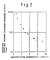
- the present inventors investigated the relationship between silicon substrate oxygen concentration and resistivity of the substrate after treatment for 1 hour in a hydrogen atmosphere at 450°C, where the substrate was a single crystal silicon substrate with an oxygen concentration of 6.0-10.0 x 10 17 atoms/cm 3 (calculated using the oxygen concentration conversion factor by the Japan Electronic Industry Development Association) and a resistivity of about 1000 ⁇ cm before heat treatment. As shown by the results in Fig.
- a SIMOX substrate employs an atmosphere with considerable oxygen during the high-temperature heat treatment step of the manufacturing process, and therefore the oxygen concentration in the substrate varies according to the solubility limit at the treatment temperature.
- the relationship between the oxygen solubility limit in single crystal silicon and the temperature is shown in Fig. 3 (J.C. Mikkelsen, Jr., THE DIFFUSIYITY AND SOLUBILITY OF OXYGEN IN SILICON, p.19-30, Materials Research Society (1986)), indicating that the solubility limit increases with increasing temperature, reaching 1.0 x 10 18 cm -3 or greater at temperatures of 1300°C and above which are normally used for high-temperature heat treatment in SIMOX substrate fabrication.
- the oxygen concentration of the SIMO X substrate varies close to the solubility limit at a given temperature during heat treatment, regardless of the oxygen concentration of the material substrate.
- the oxygen solid solution limit falls with decreasing temperature, providing a step of maintaining a temperature lowered from the maximum treatment temperature at the final stage of high-temperature heat treatment will make it possible to reduce the treatment time as well as the oxygen concentration near the solubility limit at the maintained temperature, as during the high-temperature heat treatment described above.
- 1250°C is the approximate temperature at which the oxygen solubility limit in single crystal silicon is 7.5 x 10 17 cm -3 , providing a step of maintaining a temperature of 1250°C or below for a prescribed time at the final stage of high-temperature heat treatment will render it possible to keep the oxygen concentration of the SIMOX substrate 7.5 x 10 17 cm -3 or lower. More effectively, the temperature is preferably kept at no higher than 1200°C.
- the degree of reduction in the oxygen concentration is determined by the product of the diffusion length of the oxygen dissolved in silicon at the holding temperature, and the holding time. Considering the diffusion length at 1250°C, the holding time is preferably 4 hours or longer, but from the standpoint of economy, the treatment time is preferably no longer than a maximum of 20 hours.
- the lower limit for the holding temperature is preferably 800°C.
- the atmosphere for the aforementioned step established as the final stage of the high-temperature heat treatment is not particularly restricted, as in the other steps of the high-temperature heat treatment, and it may be an inert gas such as argon or nitrogen, or alternatively oxygen, hydrogen or a mixed gas of argon/oxygen or nitrogen/oxygen.
- the apparatus used to carry out the high-temperature heat treatment is not particularly restricted so long as it can accomplish heat treatment at the prescribed temperature for the prescribed period of time.
- a high-temperature heat treatment furnace may be mentioned as a preferred typical apparatus, but so long as the functions of treatment temperature and treatment time are satisfied, the treatment may even be carried out with a lamp annealing furnace.
- the conditions in the heat treatment furnace other than the treatment temperature and treatment time, for example, the stand-by temperature, temperature ramp up and down rates, etc. are not particularly restricted, and the temperature ramp up and down conditions may also vary in stages.
- Single crystal silicon samples were produced by the Czochralski process, one with the impurity concentration controlled to 1 x 10 14 cm -3 or lower and another with it controlled to 2 x 10 13 cm -3 or lower. Each of the crystals was then worked to fabricate an 8-inch (200 mm) diameter single crystal silicon substrate.
- the resistivity of the silicon substrate immediately after fabrication was measured from the back side using the 4-point probe method, the resistivity of the substrate worked from the first crystal was 100 ⁇ cm, and the resistivity of the substrate worked from the other crystal was 500 ⁇ cm.
- the oxygen concentration was measured with a Fourier transform infrared spectrometer and found to be 8.5 x 10 17 cm -3 in both substrates.
- two of each silicon substrate were prepared, for a total of 4 substrates, which were subjected to oxygen ion implantation at a substrate temperature of 550°C, an acceleration energy of 180 keV and an implantation dose of 4 x 10 17 cm -2 .
- Pairs of the two substrates worked from different crystals were each inserted into a high-temperature heat treatment furnace for heat treatment.
- the first pair of samples A and B were heat treated for 6 hours at a temperature of 1350°C in an argon atmosphere with an oxygen partial pressure of 0.5%, after which the temperature was lowered to 800°C at a rate of 5°C/min before removal from the furnace.
- the second pair of samples C and D were heat treated for 6 hours at the same temperature of 1350°C in the same atmosphere, after which the temperature was lowered to 1250°C at a rate of 5°C/min and kept at that temperature for 4 hours. The temperature was then lowered to 800°C at a rate of 5°C/min before removal from the furnace. From the SIMOX substrate removed from the heat treatment furnace, the surface thermal oxide film was removed using a dilute hydrofluoric acid solution.
- samples A and B were found to have a surface silicon layer thickness of 340 nm and a buried oxide layer thickness of 85 nm, while samples C and D were both found to have such thicknesses of 330 nm and 85 nm, respectively.
- the resistivities of the SIMOX substrates were measured from the back side using the 4-point probe method, the values for samples A and C were 100 ⁇ cm and the values for samples B and D were 500 ⁇ cm, as for the material substrates.
- the present invention provides a high-resistance SOI substrate which has satisfactory quality and exhibits high substrate resistivity even after low-temperature heat treatment applied in device fabrication steps, by means such that the high-temperature heat treatment conditions are specified during manufacture of the SIMOX substrate using a single crystal silicon substrate with high resistivity.
Landscapes
- Element Separation (AREA)
- Crystals, And After-Treatments Of Crystals (AREA)
Abstract
Description
characterized by giving excellent layer thickness uniformity of the SOI structure obtained after high-temperature heat treatment, thereby allowing manufacture of silicon layers with satisfactory layer thickness uniformity even with thicknesses of around 0.1 µm.
| Sample | Resistivity according to 4-point probe measurement (Ωcm) | Note | |
| Before hydrogen sintering | After | ||
| A | |||
| 100 | 50 | Comp. Ex.1 | |
| B | 500 | 50 | Comp. Ex.2 |
| | 100 | 100 | Example 1 |
| D | 500 | 500 | Example 2 |
Claims (7)
- A process for fabrication of a SIMOX substrate wherein oxygen ions are implanted into a single crystal silicon substrate and then subjected to a high-temperature heat treatment to form a buried oxide layer and a surface single crystal silicon layer, the process being characterized in that the single crystal silicon substrate used has a mean resistivity of at least 100 Ωcm and no greater than the intrinsic resistivity of the single crystal silicon, and there is conducted a step of maintaining a temperature of from 800°C to 1250°C for a predetermined time in the final stage of the high-temperature heat treatment.
- The process for fabrication of a SIMOX substrate according to claim 1, characterized in that said temperature maintained in the final stage of the high-temperature heat treatment is from 800°C to 1250°C.
- The process for fabrication of a SIMOX substrate according to claim 1 or 2, characterized in that the time period for maintaining said temperature in the final stage of the high-temperature heat treatment is 4 hours or longer.
- The process for fabrication of a SIMOX substrate according to any one of claims 1 to 3, characterized in that the single crystal silicon substrate is manufactured by the Czochralski process.
- The process for fabrication of a SIMOX substrate according to any one of claims 1 to 4, characterized in that the single crystal silicon substrate used has a mean resistivity of at least 500 Ωcm and no greater than the true resistivity of the single crystal silicon.
- A SIMOX substrate fabricated by the process according to any one of claims 1 to 4, characterized in that the mean resistivity of the substrate section after a low-temperature heat treatment of said SIMOX substrate is at least 100 Ωcm and no greater than the true resistivity of the single crystal silicon.
- A SIMOX substrate fabricated by a process according to claim 5, characterized in that the mean resistivity of the substrate section after a low-temperature heat treatment of said SIMOX substrate is at least 500 Ωcm and no greater than the true resistivity of the single crystal silicon.
Applications Claiming Priority (3)
| Application Number | Priority Date | Filing Date | Title |
|---|---|---|---|
| JP2001093228 | 2001-03-28 | ||
| JP2001093228A JP2002289820A (en) | 2001-03-28 | 2001-03-28 | SIMOX substrate manufacturing method and SIMOX substrate |
| PCT/JP2002/003128 WO2002080277A1 (en) | 2001-03-28 | 2002-03-28 | Simox substrate production process and simox substrate |
Publications (3)
| Publication Number | Publication Date |
|---|---|
| EP1298731A1 true EP1298731A1 (en) | 2003-04-02 |
| EP1298731A4 EP1298731A4 (en) | 2008-04-09 |
| EP1298731B1 EP1298731B1 (en) | 2011-09-14 |
Family
ID=18947589
Family Applications (1)
| Application Number | Title | Priority Date | Filing Date |
|---|---|---|---|
| EP02707234A Expired - Lifetime EP1298731B1 (en) | 2001-03-28 | 2002-03-28 | Simox substrate production process |
Country Status (6)
| Country | Link |
|---|---|
| US (1) | US6740565B2 (en) |
| EP (1) | EP1298731B1 (en) |
| JP (1) | JP2002289820A (en) |
| KR (1) | KR100511654B1 (en) |
| TW (1) | TW541601B (en) |
| WO (1) | WO2002080277A1 (en) |
Cited By (1)
| Publication number | Priority date | Publication date | Assignee | Title |
|---|---|---|---|---|
| NL2006146C2 (en) * | 2011-02-04 | 2012-08-07 | Xycarb Ceramics B V | A method of processing substrate holder material as well as a substrate holder processed by such a method. |
Families Citing this family (5)
| Publication number | Priority date | Publication date | Assignee | Title |
|---|---|---|---|---|
| JP2005285963A (en) * | 2004-03-29 | 2005-10-13 | Sumco Corp | Manufacturing method of SOI substrate |
| JP2007005563A (en) * | 2005-06-23 | 2007-01-11 | Sumco Corp | SIMOX wafer manufacturing method |
| US8426282B2 (en) * | 2011-02-21 | 2013-04-23 | Institute of Microelectronics, Chinese Academy of Sciences | Method for forming semiconductor substrate isolation |
| FR3077924B1 (en) * | 2018-02-13 | 2020-01-17 | Soitec | REMOVABLE STRUCTURE AND DISASSEMBLY METHOD USING THE SAME |
| JP7666396B2 (en) * | 2022-05-12 | 2025-04-22 | 信越半導体株式会社 | Method for detecting crystal defects in silicon single crystal substrate |
Family Cites Families (11)
| Publication number | Priority date | Publication date | Assignee | Title |
|---|---|---|---|---|
| JPS5856344A (en) | 1981-09-29 | 1983-04-04 | Fujitsu Ltd | Manufacture of semiconductor device |
| JPS62202528A (en) * | 1986-03-03 | 1987-09-07 | Toshiba Corp | Manufacture of semiconductor substrate |
| JP3036619B2 (en) * | 1994-03-23 | 2000-04-24 | コマツ電子金属株式会社 | SOI substrate manufacturing method and SOI substrate |
| JP3204855B2 (en) | 1994-09-30 | 2001-09-04 | 新日本製鐵株式会社 | Semiconductor substrate manufacturing method |
| JPH0964320A (en) | 1995-08-29 | 1997-03-07 | Hitachi Ltd | SOI substrate, semiconductor device using the same, and method of manufacturing the same |
| JP3762144B2 (en) * | 1998-06-18 | 2006-04-05 | キヤノン株式会社 | Method for manufacturing SOI substrate |
| JP2000082679A (en) * | 1998-07-08 | 2000-03-21 | Canon Inc | Semiconductor substrate and manufacturing method thereof |
| EP1087041B1 (en) * | 1999-03-16 | 2009-01-07 | Shin-Etsu Handotai Co., Ltd | Production method for silicon wafer and silicon wafer |
| JP3870293B2 (en) | 1999-03-26 | 2007-01-17 | シルトロニック・ジャパン株式会社 | Silicon semiconductor substrate and manufacturing method thereof |
| JP2000281490A (en) | 1999-03-26 | 2000-10-10 | Nippon Steel Corp | Silicon semiconductor substrate and method of manufacturing the same |
| EP1423871A2 (en) * | 2001-06-22 | 2004-06-02 | MEMC Electronic Materials, Inc. | Process for producing silicon on insulator structure having intrinsic gettering by ion implantation |
-
2001
- 2001-03-28 JP JP2001093228A patent/JP2002289820A/en active Pending
-
2002
- 2002-03-28 WO PCT/JP2002/003128 patent/WO2002080277A1/en not_active Ceased
- 2002-03-28 KR KR10-2002-7015978A patent/KR100511654B1/en not_active Expired - Fee Related
- 2002-03-28 TW TW091106214A patent/TW541601B/en not_active IP Right Cessation
- 2002-03-28 US US10/296,858 patent/US6740565B2/en not_active Expired - Lifetime
- 2002-03-28 EP EP02707234A patent/EP1298731B1/en not_active Expired - Lifetime
Cited By (3)
| Publication number | Priority date | Publication date | Assignee | Title |
|---|---|---|---|---|
| NL2006146C2 (en) * | 2011-02-04 | 2012-08-07 | Xycarb Ceramics B V | A method of processing substrate holder material as well as a substrate holder processed by such a method. |
| EP2485252A1 (en) | 2011-02-04 | 2012-08-08 | Xycarb Ceramics B.V. | A method of processing substrate holder material |
| US9362157B2 (en) | 2011-02-04 | 2016-06-07 | Xycarb Ceramics B.V. | Method of processing substrate holder material as well as substrate holder processed by such method |
Also Published As
| Publication number | Publication date |
|---|---|
| KR20030007704A (en) | 2003-01-23 |
| US20030170940A1 (en) | 2003-09-11 |
| KR100511654B1 (en) | 2005-09-01 |
| WO2002080277A1 (en) | 2002-10-10 |
| US6740565B2 (en) | 2004-05-25 |
| JP2002289820A (en) | 2002-10-04 |
| EP1298731B1 (en) | 2011-09-14 |
| TW541601B (en) | 2003-07-11 |
| EP1298731A4 (en) | 2008-04-09 |
Similar Documents
| Publication | Publication Date | Title |
|---|---|---|
| CN103430298B (en) | Silicon-on-insulator structures having regions of high resistivity in a handle wafer and methods of fabricating such structures | |
| CN114093764B (en) | Single crystal silicon wafer | |
| KR101340002B1 (en) | SOI Wafer Manufacturing Method | |
| JPWO2005024925A1 (en) | Manufacturing method of SOI wafer | |
| EP0817248A2 (en) | Method of manufacturing SOI substrate | |
| JP3033655B2 (en) | Semiconductor device and method of manufacturing semiconductor device | |
| US20080164572A1 (en) | Semiconductor substrate and manufacturing method thereof | |
| EP1298731B1 (en) | Simox substrate production process | |
| US20100052093A1 (en) | Semiconductor substrate and method of manufacturing the same | |
| CN115552592B (en) | Method of manufacturing a semiconductor-on-insulator substrate for radio frequency applications | |
| EP1391931A1 (en) | Soi substrate | |
| CN100472710C (en) | Semiconductor substrate and manufacturing method thereof | |
| US12588445B2 (en) | Methods of manufacturing semiconductor devices and semiconductor devices | |
| TWI911218B (en) | Process for fabricating a semiconductor-on-insulator substrate for radiofrequency applications | |
| JP2005175390A (en) | Simox substrate and its manufacturing method | |
| WO2011118205A1 (en) | Process for producing soi wafer | |
| JP2000068489A (en) | SOI substrate and method of manufacturing the same | |
| JP2002289819A (en) | SIMOX substrate | |
| JP2008159868A (en) | Method for manufacturing simox substrate |
Legal Events
| Date | Code | Title | Description |
|---|---|---|---|
| PUAI | Public reference made under article 153(3) epc to a published international application that has entered the european phase |
Free format text: ORIGINAL CODE: 0009012 |
|
| 17P | Request for examination filed |
Effective date: 20021128 |
|
| AK | Designated contracting states |
Kind code of ref document: A1 Designated state(s): AT BE CH CY DE DK ES FI FR GB GR IE IT LI LU MC NL PT SE TR Designated state(s): AT BE CH CY DE DK ES FI FR GB GR IE IT LI LU MC NL PT SE TR |
|
| A4 | Supplementary search report drawn up and despatched |
Effective date: 20080306 |
|
| 17Q | First examination report despatched |
Effective date: 20080718 |
|
| GRAP | Despatch of communication of intention to grant a patent |
Free format text: ORIGINAL CODE: EPIDOSNIGR1 |
|
| RTI1 | Title (correction) |
Free format text: SIMOX SUBSTRATE PRODUCTION PROCESS |
|
| GRAS | Grant fee paid |
Free format text: ORIGINAL CODE: EPIDOSNIGR3 |
|
| GRAA | (expected) grant |
Free format text: ORIGINAL CODE: 0009210 |
|
| RAP1 | Party data changed (applicant data changed or rights of an application transferred) |
Owner name: NIPPON STEEL CORPORATION |
|
| AK | Designated contracting states |
Kind code of ref document: B1 Designated state(s): DE FR GB IT |
|
| REG | Reference to a national code |
Ref country code: GB Ref legal event code: FG4D |
|
| REG | Reference to a national code |
Ref country code: DE Ref legal event code: R096 Ref document number: 60241019 Country of ref document: DE Effective date: 20111110 |
|
| PLBE | No opposition filed within time limit |
Free format text: ORIGINAL CODE: 0009261 |
|
| STAA | Information on the status of an ep patent application or granted ep patent |
Free format text: STATUS: NO OPPOSITION FILED WITHIN TIME LIMIT |
|
| 26N | No opposition filed |
Effective date: 20120615 |
|
| REG | Reference to a national code |
Ref country code: DE Ref legal event code: R097 Ref document number: 60241019 Country of ref document: DE Effective date: 20120615 |
|
| REG | Reference to a national code |
Ref country code: DE Ref legal event code: R081 Ref document number: 60241019 Country of ref document: DE Owner name: NIPPON STEEL & SUMITOMO METAL CORPORATION, JP Free format text: FORMER OWNER: NIPPON STEEL CORPORATION, TOKIO/TOKYO, JP Effective date: 20130227 Ref country code: DE Ref legal event code: R082 Ref document number: 60241019 Country of ref document: DE Representative=s name: VOSSIUS & PARTNER, DE Effective date: 20130227 Ref country code: DE Ref legal event code: R081 Ref document number: 60241019 Country of ref document: DE Owner name: NIPPON STEEL & SUMITOMO METAL CORPORATION, JP Free format text: FORMER OWNER: NIPPON STEEL CORP., TOKIO/TOKYO, JP Effective date: 20110920 Ref country code: DE Ref legal event code: R082 Ref document number: 60241019 Country of ref document: DE Representative=s name: VOSSIUS & PARTNER PATENTANWAELTE RECHTSANWAELT, DE Effective date: 20130227 |
|
| REG | Reference to a national code |
Ref country code: FR Ref legal event code: CA Effective date: 20130913 Ref country code: FR Ref legal event code: CD Owner name: NIPPON STEEL & SUMITOMO METAL CORPORATION, JP Effective date: 20130913 |
|
| REG | Reference to a national code |
Ref country code: FR Ref legal event code: PLFP Year of fee payment: 15 |
|
| REG | Reference to a national code |
Ref country code: FR Ref legal event code: PLFP Year of fee payment: 16 |
|
| REG | Reference to a national code |
Ref country code: FR Ref legal event code: PLFP Year of fee payment: 17 |
|
| PGFP | Annual fee paid to national office [announced via postgrant information from national office to epo] |
Ref country code: IT Payment date: 20190326 Year of fee payment: 18 Ref country code: DE Payment date: 20190312 Year of fee payment: 18 Ref country code: GB Payment date: 20190327 Year of fee payment: 18 |
|
| PGFP | Annual fee paid to national office [announced via postgrant information from national office to epo] |
Ref country code: FR Payment date: 20190213 Year of fee payment: 18 |
|
| REG | Reference to a national code |
Ref country code: DE Ref legal event code: R082 Ref document number: 60241019 Country of ref document: DE Representative=s name: VOSSIUS & PARTNER PATENTANWAELTE RECHTSANWAELT, DE Ref country code: DE Ref legal event code: R081 Ref document number: 60241019 Country of ref document: DE Owner name: NIPPON STEEL CORPORATION, JP Free format text: FORMER OWNER: NIPPON STEEL & SUMITOMO METAL CORPORATION, TOKYO, JP |
|
| REG | Reference to a national code |
Ref country code: DE Ref legal event code: R119 Ref document number: 60241019 Country of ref document: DE |
|
| PG25 | Lapsed in a contracting state [announced via postgrant information from national office to epo] |
Ref country code: FR Free format text: LAPSE BECAUSE OF NON-PAYMENT OF DUE FEES Effective date: 20200331 Ref country code: DE Free format text: LAPSE BECAUSE OF NON-PAYMENT OF DUE FEES Effective date: 20201001 |
|
| GBPC | Gb: european patent ceased through non-payment of renewal fee |
Effective date: 20200328 |
|
| PG25 | Lapsed in a contracting state [announced via postgrant information from national office to epo] |
Ref country code: GB Free format text: LAPSE BECAUSE OF NON-PAYMENT OF DUE FEES Effective date: 20200328 |
|
| PG25 | Lapsed in a contracting state [announced via postgrant information from national office to epo] |
Ref country code: IT Free format text: LAPSE BECAUSE OF NON-PAYMENT OF DUE FEES Effective date: 20200328 |