EP1298714A1 - Method of manufacturing compound semiconductor wafer - Google Patents
Method of manufacturing compound semiconductor wafer Download PDFInfo
- Publication number
- EP1298714A1 EP1298714A1 EP02701687A EP02701687A EP1298714A1 EP 1298714 A1 EP1298714 A1 EP 1298714A1 EP 02701687 A EP02701687 A EP 02701687A EP 02701687 A EP02701687 A EP 02701687A EP 1298714 A1 EP1298714 A1 EP 1298714A1
- Authority
- EP
- European Patent Office
- Prior art keywords
- wafer
- wafers
- polishing
- obverse
- adsorption pad
- Prior art date
- Legal status (The legal status is an assumption and is not a legal conclusion. Google has not performed a legal analysis and makes no representation as to the accuracy of the status listed.)
- Withdrawn
Links
Images



Classifications
-
- H—ELECTRICITY
- H10—SEMICONDUCTOR DEVICES; ELECTRIC SOLID-STATE DEVICES NOT OTHERWISE PROVIDED FOR
- H10P—GENERIC PROCESSES OR APPARATUS FOR THE MANUFACTURE OR TREATMENT OF DEVICES COVERED BY CLASS H10
- H10P70/00—Cleaning of wafers, substrates or parts of devices
- H10P70/10—Cleaning before device manufacture, i.e. Begin-Of-Line process
- H10P70/15—Cleaning before device manufacture, i.e. Begin-Of-Line process by wet cleaning only
-
- H—ELECTRICITY
- H10—SEMICONDUCTOR DEVICES; ELECTRIC SOLID-STATE DEVICES NOT OTHERWISE PROVIDED FOR
- H10P—GENERIC PROCESSES OR APPARATUS FOR THE MANUFACTURE OR TREATMENT OF DEVICES COVERED BY CLASS H10
- H10P52/00—Grinding, lapping or polishing of wafers, substrates or parts of devices
-
- B—PERFORMING OPERATIONS; TRANSPORTING
- B24—GRINDING; POLISHING
- B24B—MACHINES, DEVICES, OR PROCESSES FOR GRINDING OR POLISHING; DRESSING OR CONDITIONING OF ABRADING SURFACES; FEEDING OF GRINDING, POLISHING, OR LAPPING AGENTS
- B24B37/00—Lapping machines or devices; Accessories
- B24B37/04—Lapping machines or devices; Accessories designed for working plane surfaces
- B24B37/042—Lapping machines or devices; Accessories designed for working plane surfaces operating processes therefor
-
- B—PERFORMING OPERATIONS; TRANSPORTING
- B24—GRINDING; POLISHING
- B24B—MACHINES, DEVICES, OR PROCESSES FOR GRINDING OR POLISHING; DRESSING OR CONDITIONING OF ABRADING SURFACES; FEEDING OF GRINDING, POLISHING, OR LAPPING AGENTS
- B24B37/00—Lapping machines or devices; Accessories
- B24B37/27—Work carriers
- B24B37/30—Work carriers for single side lapping of plane surfaces
-
- H—ELECTRICITY
- H10—SEMICONDUCTOR DEVICES; ELECTRIC SOLID-STATE DEVICES NOT OTHERWISE PROVIDED FOR
- H10P—GENERIC PROCESSES OR APPARATUS FOR THE MANUFACTURE OR TREATMENT OF DEVICES COVERED BY CLASS H10
- H10P90/00—Preparation of wafers not covered by a single main group of this subclass, e.g. wafer reinforcement
- H10P90/12—Preparing bulk and homogeneous wafers
- H10P90/129—Preparing bulk and homogeneous wafers by polishing
Definitions
- the present invention relates to methods of manufacturing compound semiconductor wafers. It relates in particular to a method for polishing sliced wafers to a mirrorlike finish, and to a novel method for post-polishing wafer storage.
- a "compound semiconductor” means a semiconductor that is of a compound such as gallium arsenide (GaAs), indium phosphate (InP), or gallium phosphate (GaP). From polycrystalline raw materials, single crystals are grown by a crystal-growth technique such as the vertical boat (VB) method, liquid-encapsulated Czochralski (LEC) method, or horizontal Bridgman (HB) method. A single-crystal ingot is sliced into thin slices to produce "as-cut” wafers. These are processed through procedures such as pre-processing, polishing, cleaning, inspection/measuring, and final cleaning procedures, and shipped as "mirror wafers" to the device manufacturer.
- VB vertical boat
- LEC liquid-encapsulated Czochralski
- a compound semiconductor wafer manufacturing method is as follows.
- a cylindrical single-crystal ingot is grown from a polycrystalline raw material using single-crystal-growing equipment such as an LEC device, an HB device, or a VB device.
- Single-crystal ingots that do not turn out cylindrical are ground into a cylinder.
- the cylindrical single-crystal ingot is sliced through a plane perpendicular to its axis, rendering an as-cut wafer of constant thickness.
- the ridgeline along the wafer circumferentially is then thinly shaved obliquely. This is called chamfering or beveling.
- This wafer is treated by etching-lapping- etching processes.
- the etching process at the beginning removes manufacturing distortions; the lapping process makes the thickness a predetermined depth; the etching process at the end removes distortions due to lapping.
- the initial etching process can be left out. A beveled wafer of constant thickness is thus produced.
- a polishing-preprocess procedure (a); a polishing procedure (b); a cleaning procedure (c); an inspection/measuring procedure (d); and a final cleaning procedure (e).
- a single procedure includes a plurality of processes. To the end of the word "process,” “operation,” “step,” or nothing at all, will be affixed. Procedure and process should not be confused.
- mirror wafers are fabricated, and are shipped in that state to the device maker.
- the device maker cannot use them as substrates for thin-film growing (layering). This is because in the course after being packaged and until reaching the device maker they become oxidized, contaminated, and dirtied with adhering particles. Therefore, prior to thin-film growing the wafers have had to be etched and cleaned on the manufacturer's end.
- Prior Art I., Japanese Pub. Pat. App. No. H11-204471, "Compound Semiconductor Wafer Manufacturing Method,” provides for oxidizing using ozone after polishing a semiconductor wafer and before drying and cleaning.
- An oxide layer that is 1.5 nm or more in thickness is said to be satisfactory.
- Fashioning the oxide layer leads to debris riding onto the oxide layer on the wafer.
- cleaning using alkali to get rid of the oxide layer and at once to get rid of the debris is then provided for. This means that the obverse surface will become clean, since removing the oxide layer also removes the debris thereon.
- One object of the present invention is to resolve drawbacks as in the foregoing, by providing a wafer manufacturing method through which there is no possibility of the wafers being contaminated by organic matter, such as wax, used for joining.
- Another object of the present invention is to provide a wafer manufacturing method in which the use of organic solvent is reduced to contribute significantly to environmental protection.
- Yet another object of the present invention is to provide a wafer manufacturing method rendered so as not to give rise to quality-deteriorating factors-such as adherence of debris, oxidization, or alteration-due to post-polish drying of the wafers in the atmosphere.
- a further object of the present invention is to provide a wafer manufacturing method that enables the fabrication of wafers having an advanced degree of cleanness without requiring re-cleaning at the shipping destination (device maker).
- a method under the present invention of manufacturing a compound semiconductor wafer are that the wafers are, without using an organic joining material, adsorbed onto an adsorption pad and mirror-polished, and the post-mirror-polished wafers are stored in water within an ultra-purified water vat.
- the wafers that have been stored within water are, with no cleaning in organic solvent, alkali washed, purified-water washed, and dried to produce clean, mirror-polished wafers.
- the wafers are adsorbed onto an adsorption pad without in the least using wax or any other organic joining material.
- One other is that the storing into water is without post-polish drying-which is not atmospheric storage, but aquatic storage. There are thus two features, each with superior effects.
- aquatic storage is epochal.
- post-polish drying is detrimental in that it leads to adherence of foreign matter, and to alteration of the wafer obverse surface.
- the present invention since the wafers without being dried are aquatically stored in a purified water vat, the problem of the wafers getting smudged while drying disappears. Problems with the wafer surface oxidizing/altering while drying, or else with foreign matter firmly clinging to the wafers may be solved.
- the storage method is truly unconventional and surpassing.
- Adsorption pads themselves are publicly known, and have been developed for non-wax wafer polishing. They are sometimes also referred to as "packing pads” or “templates.” They are thin porous sheets of plastic and are adhered to a metal jig such as a polishing plate with, e.g., adhesive tape. They are pliant materials with flatness nonetheless. To attach wafers to the pads, organic joining material such as wax is not needed.
- certain pads are such that the wafer is wet with water and pressed onto the pad. After polishing the wafer may be detached with a spatula. Alternatively, the pad is heated and the wafer is pressed on. After polishing it is cooled and the wafer is removed with a spatula. Because it is suitably pliant, the adsorption pad retains the wafer gently. The holding power against slipping is, however, not strong in the way that wax is. Therefore, a shallow wafer-mounting hole whose diameter is about equal to the size of the wafer is formed in the polishing plate, and the adsorption pad is fixed into the wafer-mounting hole.
- the adsorption pad thickness is d
- the hole depth is t
- the wafer thickness is w
- the mounting hole retains that much (d + w- t ) of the wafer circumferential surface that is in excess of the hole depth. Accordingly, when the polishing plate is pressed onto the polishing platen and the platen is rotated, the wafers on the polishing plate become polished.
- the adsorption pad has been described.
- the present invention uses an adsorption pad for non-wax polishing of wafers.
- Non-wax polishing though a new technology, is previously known publicly; and the adsorption pad itself is not novel.
- polishing that uses a conventional adsorption pad to date has been the post-polish drying and atmospheric storage in Fig. 1. It has therefore not been possible to overcome the drawbacks of debris adhering to the wafers, the surface oxidizing, and the surface altering. Debris stuck on a water-wet wafer agglutinates after drying and is hard to get off. When devices are built on the surface, alteration therein produces inconsistencies in the characteristics. While surface oxidization is said to be gotten rid of by alkali treatment, even though the oxidization film may be removed with alkali, since it is thick and not uniform, jaggedness appears.
- the present invention is non-wax wafer polishing using adsorption pads, and storage of the wafers in water, and so is strikingly capable of ingeniously preventing wafer contamination, oxidization and alteration. Inasmuch as the wafers are stored in water, particles do not adhere, the surface does not oxidize, nor does the surface alter, which would not be the case but for the fact that adsorption pads are employed.
- aquatic storage done with wax-employing polishing is meaningless.
- the significance of aquatic storage begins with non-wax polishing.
- the present invention eliminates finishing polish done (mirror polishing) according to the organic-compound- (wax-) applying plate-paste process.
- the wafers are retained utilizing adsorption pads instead. Chemical-solvent cleaning becomes unnecessary. Since the wafers are stored in water, surface degradation such as particle adherence, oxidization, and alteration does not occur. Wafers with uncontaminated surfaces are gained.
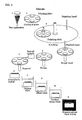
- Figs. 1 and 3 a wafer manufacturing method under the present invention will be explained in contrast to a conventional method. Processes that are the same as those of the conventional technique are labeled with the same reference marks.
- One wafer is tacked onto a single polishing plate in Fig. 3.
- some polishing plates are single-wafer, and some are multiple-wafer.
- An adsorption pad made from a flexible material having a flat and smooth surface is glued onto the back surface of the polishing plate, and against it a water-wet wafer or a heated wafer is pressed, adsorbing the wafer onto the pad. Wax is unnecessary. Whether the wafer is heated or immersed in water depends on the properties of the adsorption pad.
- the wafer surface that is exposed to the exterior is the obverse face.
- the polishing plate is a jig being a disk atop which a shaft is fixed.
- the wafer surfaces are oxidized by and alter due to oxygen and minute amounts of chemical substances in the air.
- aerial drying and storage is the danger of oxidization and alteration of, and debris adherence to, the wafers.
- storing in ultra-purified water eliminates the risk of oxidization and alteration. This is because there is neither oxygen nor chemical substances in ultra-purified water. What is more, there is no adhering of particles.
- aquatic storage is flawless. It is a perfect method in eliminating oxidization and alteration of, and debris adherence to, the wafers as just mentioned, and the present invention in presenting this is very unconventional and epochal.
- the polishing liquid is sufficiently gotten rid of while cleaning, contamination may be decreased still further.
- GaAs ingots were sliced into rounds, etched and lapped. These were adsorbed onto an adsorption pad on a polishing plate and pressed against a rotary platen; by spinning the platen while flowing a polishing liquid on them the wafers were polished.
- the wafers were undone from the adsorption pad. With a simple cleaning and without drying they were aquatically stored within ultra-purified water. Thereafter they were alkali washed, purified-water washed, and spin-dried. Then, based on specifications from the shipping destination, they were inspected and measured. Thereafter they were given an alkali wash, a purified-water wash, and a spin dry.
- mirror wafers This yielded mirror wafers.
- the mirror wafers were examined under a microscope. It was confirmed that the obverse surfaces were completely cleared of residual organic matter, and that they were uncontaminated mirror wafers free of alterations in and oxidized films on the mirror-like face, and of adhered particles.
- GaAs wafers were fabricated by the conventional fabrication procedures (Fig. 1 left side; Fig. 2).
- a thin film was grown directly onto the substrates without likewise carrying out the thin-film growth preprocess procedure (etching, cleaning) on wafers according to the conventional technique.
- Foreign matter between the obverse surface and the thin film was assayed, whereupon the presence of residual foreign matter was confirmed.
- the present invention carries out wafer polishing by means of a polishing plate that does not use wax, and aquatically stores without drying the post-polished wafers undone from the polishing plate. Inasmuch as the drying process is omitted, there is no obverse surface oxidation, obverse surface alteration, nor debris adherence. Inasmuch as no wax is used, there is no residual organic matter.
- the present invention enables, markedly more so than conventionally, the fabrication of high-quality, uncontaminated mirror wafers. This thereby enables omitting on the device-maker end (the shipping destination) preprocessing, such as etching and cleaning, for thin-film formation. A further advantage is that abnormal growth appearing when thin films are grown on top of conventional-technique wafers does not occur.
- the vertical scale is relative scores for obverse-surface foreign-matter counts on wafers from the conventional technique (expressed in percentages; 100% being the prior-art level), wherein the average of the obverse-surface foreign-matter counts is taken to be 100.
- a horizontal line has been drawn at the average level for obverse-surface foreign-matter counts on wafers from the conventional technique.
- a horizontal line is also drawn at the average of the obverse-surface foreign-matter counts on wafers by the present invention.
- the foreign-matter counts (particles) on the wafers from the conventional technique are larger. Likewise, fluctuation in the foreign-matter count is greater.
- the particle score for No. 8 was 222%; for No. 9, 206%; and for No. 7, 203%. For Nos. 42 and 37 there was 140% obverse-surface foreign matter. Oppositely, the particle score was about 41% for wafers No. 49 and 53.
- the foreign-matter counts (particles) on the wafers from the present invention are slight, and foreign-matter count fluctuations are small.
- Nos. 5, 31, 42, 43, 46 and 58 are the slightest at 27%.
- the average obverse-surface foreign-matter count (particle score) for wafers from the present invention was 45%, meaning that it decreased to around 45% of the conventional technique by comparison. A decrease like this in obverse-surface foreign-matter count attests as described to the superiority of the present invention.
- the thicknesses of obverse-surface oxidization films in the same 60-wafers-apiece sample groups were gauged.
- the obverse-surface oxidization film thickness average for wafers by the conventional technique was 1.0 nm.
- the oxidization-film average thickness for wafers by the present invention was 0.7 nm, meaning that the oxidization film became about 0.3 nm thinner. This is an effect of aquatic storage. Inasmuch as the wafers were brought out into the air and dried following aquatic storage, the obverse surface did oxidize slightly, as would be expected.
Landscapes
- Engineering & Computer Science (AREA)
- Mechanical Engineering (AREA)
- Mechanical Treatment Of Semiconductor (AREA)
Abstract
Description
Claims (6)
- A compound-semiconductor-wafer manufacturing method characterized in that a compound semiconductor wafer is without using organic material adsorbently fixed to a polishing plate to which an adsorption pad is bonded, pressed against a polishing platen and polished, and taken off the polishing plate and aquatically stored within purified water without being dried.
- The compound-semiconductor-wafer manufacturing method set forth in claim 1, characterized in that a cleaning procedure for cleaning the aquatically stored wafer does not include organic solvent washing.
- The compound-semiconductor-wafer manufacturing method set forth in claim 1 or 2, characterized in that the wafer is held fast to the adsorption pad by means of water surface tension by dripping water onto a smooth surface that the adsorption pad has and pressing the wafer onto the adsorption pad.
- The compound-semiconductor-wafer manufacturing method set forth in any of claims 1 through 3, characterized in that a template having a hole 0.2 mm to 0.8 mm diametrically larger than the wafer diameter is mounted onto the adsorption pad when polishing, and the wafer is fixed to the adsorption pad surface within the template hole.
- The compound-semiconductor-wafer manufacturing method set forth in any of claims 1 through 4, characterized in that after cleaning the aquatically stored wafers they are dried by spin-drying.
- The compound-semiconductor-wafer manufacturing method set forth in any of claims 1 through 5, characterized in that preprocessing is not done for thin-film growing.
Applications Claiming Priority (3)
| Application Number | Priority Date | Filing Date | Title |
|---|---|---|---|
| JP2001061178 | 2001-03-06 | ||
| JP2001061178A JP2002261058A (en) | 2001-03-06 | 2001-03-06 | Method for manufacturing compound semiconductor wafer |
| PCT/JP2002/001936 WO2002071461A1 (en) | 2001-03-06 | 2002-03-01 | Method of manufacturing compound semiconductor wafer |
Publications (2)
| Publication Number | Publication Date |
|---|---|
| EP1298714A1 true EP1298714A1 (en) | 2003-04-02 |
| EP1298714A4 EP1298714A4 (en) | 2006-05-24 |
Family
ID=18920510
Family Applications (1)
| Application Number | Title | Priority Date | Filing Date |
|---|---|---|---|
| EP02701687A Withdrawn EP1298714A4 (en) | 2001-03-06 | 2002-03-01 | PROCESS FOR PRODUCING COMPOUND SEMICONDUCTORS |
Country Status (7)
| Country | Link |
|---|---|
| EP (1) | EP1298714A4 (en) |
| JP (1) | JP2002261058A (en) |
| KR (1) | KR20020093134A (en) |
| CN (1) | CN100405553C (en) |
| CA (1) | CA2406424A1 (en) |
| TW (1) | TW569329B (en) |
| WO (1) | WO2002071461A1 (en) |
Families Citing this family (11)
| Publication number | Priority date | Publication date | Assignee | Title |
|---|---|---|---|---|
| JP2006261473A (en) * | 2005-03-18 | 2006-09-28 | National Institute Of Advanced Industrial & Technology | Storage method of silicon substrate on which silicon oxide film is formed |
| CN100522478C (en) * | 2006-08-22 | 2009-08-05 | 北京有色金属研究总院 | Double-side polishing method for gallium phosphide wafer |
| CN105014520B (en) * | 2015-08-13 | 2017-10-27 | 江苏吉星新材料有限公司 | A kind of sapphire substrate sheet immersion cmp method |
| JP6938084B2 (en) * | 2017-07-26 | 2021-09-22 | 株式会社ディスコ | Blade holder |
| CN108000356A (en) * | 2017-11-20 | 2018-05-08 | 杭州智谷精工有限公司 | A kind of aspheric-surface workpiece clamp method |
| CN107984383A (en) * | 2017-11-20 | 2018-05-04 | 杭州智谷精工有限公司 | A kind of planar part clamp method |
| CN108000243A (en) * | 2017-11-20 | 2018-05-08 | 杭州智谷精工有限公司 | A kind of biplane Polishing machining method |
| CN108015666A (en) * | 2017-11-20 | 2018-05-11 | 杭州智谷精工有限公司 | A kind of monoplane Polishing machining method |
| CN107993921A (en) * | 2017-11-27 | 2018-05-04 | 上海超硅半导体有限公司 | Curing means and maintaining process after a kind of wafer polishing |
| CN110379759B (en) * | 2019-07-05 | 2021-02-02 | 深超光电(深圳)有限公司 | Adsorption device, transfer system and transfer method |
| CN112720226A (en) * | 2020-12-29 | 2021-04-30 | 广东先导先进材料股份有限公司 | Wax-free polishing method for ultrathin semiconductor wafer |
Family Cites Families (11)
| Publication number | Priority date | Publication date | Assignee | Title |
|---|---|---|---|---|
| JPH04101418A (en) * | 1990-08-20 | 1992-04-02 | Kyushu Electron Metal Co Ltd | Method of increasing lifetime of si wafer |
| JPH04213825A (en) * | 1990-12-11 | 1992-08-04 | Sumitomo Electric Ind Ltd | Manufacture of compound semiconductor device |
| JPH05166785A (en) * | 1991-12-18 | 1993-07-02 | Nikko Kyodo Co Ltd | Storing method for semiconductor wafer |
| JPH06151304A (en) * | 1992-11-13 | 1994-05-31 | Toshiba Corp | Compound semiconductor wafer |
| US5571373A (en) * | 1994-05-18 | 1996-11-05 | Memc Electronic Materials, Inc. | Method of rough polishing semiconductor wafers to reduce surface roughness |
| JPH09270401A (en) * | 1996-01-31 | 1997-10-14 | Shin Etsu Handotai Co Ltd | Polishing method for semiconductor wafer |
| JPH09262763A (en) * | 1996-03-28 | 1997-10-07 | Shin Etsu Handotai Co Ltd | Method and apparatus for manufacturing backing pad |
| JP3257518B2 (en) * | 1997-12-26 | 2002-02-18 | 信越半導体株式会社 | How to store silicon wafers in liquid |
| US6884721B2 (en) | 1997-12-25 | 2005-04-26 | Shin-Etsu Handotai Co., Ltd. | Silicon wafer storage water and silicon wafer storage method |
| JP3255103B2 (en) * | 1997-12-25 | 2002-02-12 | 信越半導体株式会社 | Storage water for silicon wafers and method of storage |
| JP2000308961A (en) * | 1999-04-26 | 2000-11-07 | Speedfam-Ipec Co Ltd | Adhesive plate and its manufacturing method |
-
2001
- 2001-03-06 JP JP2001061178A patent/JP2002261058A/en active Pending
-
2002
- 2002-03-01 KR KR1020027014854A patent/KR20020093134A/en not_active Ceased
- 2002-03-01 CN CNB028005376A patent/CN100405553C/en not_active Expired - Fee Related
- 2002-03-01 EP EP02701687A patent/EP1298714A4/en not_active Withdrawn
- 2002-03-01 CA CA002406424A patent/CA2406424A1/en not_active Abandoned
- 2002-03-01 WO PCT/JP2002/001936 patent/WO2002071461A1/en not_active Ceased
- 2002-03-06 TW TW091104134A patent/TW569329B/en not_active IP Right Cessation
Also Published As
| Publication number | Publication date |
|---|---|
| KR20020093134A (en) | 2002-12-12 |
| JP2002261058A (en) | 2002-09-13 |
| CN100405553C (en) | 2008-07-23 |
| WO2002071461A1 (en) | 2002-09-12 |
| CN1457507A (en) | 2003-11-19 |
| EP1298714A4 (en) | 2006-05-24 |
| TW569329B (en) | 2004-01-01 |
| CA2406424A1 (en) | 2002-10-16 |
Similar Documents
| Publication | Publication Date | Title |
|---|---|---|
| JP5628224B2 (en) | Method for polishing a substrate surface | |
| US6899762B2 (en) | Epitaxially coated semiconductor wafer and process for producing it | |
| US4588473A (en) | Semiconductor wafer process | |
| US6861360B2 (en) | Double-sided polishing process for producing a multiplicity of silicon semiconductor wafers | |
| JP6206360B2 (en) | Polishing method of silicon wafer | |
| US20010014570A1 (en) | Process for producing a semiconductor wafer with polished edge | |
| JP2000235941A (en) | Semiconductor wafer, method of manufacturing semiconductor wafer, and use of the method | |
| KR102117362B1 (en) | Silicon wafer polishing method and silicon wafer manufacturing method | |
| JP2001358095A (en) | Semiconductor wafer double-side polishing method and carrier for carrying out the method | |
| JPH11502674A (en) | Single etch stop method for the manufacture of silicon-on-insulator wafers | |
| JP2006222453A (en) | Silicon wafer manufacturing method, silicon wafer, and SOI wafer | |
| CN104952701B (en) | A kind of abnormity semiconductor wafer and preparation method thereof | |
| CA2406424A1 (en) | Method of manufacturing compound semiconductor wafer | |
| US20010039101A1 (en) | Method for converting a reclaim wafer into a semiconductor wafer | |
| US7078343B2 (en) | Method of manufacturing compound semiconductor wafer | |
| US4184908A (en) | Method for polishing cadmium sulfide semiconductors | |
| JPH11191544A (en) | Semiconductor substrate and method of manufacturing the same | |
| CN118438300A (en) | Pretreatment method for soft and brittle crystal before fine polishing | |
| JP2000243796A (en) | Method for measuring contaminants on semiconductor wafer surface | |
| JP4168546B2 (en) | Epitaxial wafer for semiconductor light emitting device and method for manufacturing semiconductor light emitting device | |
| JP3014152B2 (en) | Method for manufacturing semiconductor wafer | |
| JPH0297500A (en) | GaAs single crystal mirror wafer and its manufacturing method | |
| JP4128687B2 (en) | Semiconductor wafer surface cleanliness management method and etching allowance detection method | |
| JP3718419B2 (en) | Manufacturing method of silicon epitaxial wafer | |
| JPH06342839A (en) | Method of inspecting layer feebly modified by treatment on surface of silicon wafer, and method of measuring its thickness |
Legal Events
| Date | Code | Title | Description |
|---|---|---|---|
| PUAI | Public reference made under article 153(3) epc to a published international application that has entered the european phase |
Free format text: ORIGINAL CODE: 0009012 |
|
| 17P | Request for examination filed |
Effective date: 20021106 |
|
| AK | Designated contracting states |
Kind code of ref document: A1 Designated state(s): AT BE CH CY DE DK ES FI FR GB GR IE IT LI LU MC NL PT SE TR Designated state(s): AT BE CH CY DE DK ES FI FR GB GR IE IT LI LU MC NL PT SE TR |
|
| AX | Request for extension of the european patent |
Extension state: AL LT LV MK RO SI |
|
| A4 | Supplementary search report drawn up and despatched |
Effective date: 20060406 |
|
| RIC1 | Information provided on ipc code assigned before grant |
Ipc: H01L 21/306 20060101ALI20060401BHEP Ipc: B24B 37/04 20060101ALI20060401BHEP Ipc: H01L 21/304 20060101AFI20020913BHEP |
|
| 17Q | First examination report despatched |
Effective date: 20090518 |
|
| STAA | Information on the status of an ep patent application or granted ep patent |
Free format text: STATUS: THE APPLICATION IS DEEMED TO BE WITHDRAWN |
|
| 18D | Application deemed to be withdrawn |
Effective date: 20110409 |