EP1298710A1 - Method for protecting a tungsten element in semiconductor device fabrication - Google Patents
Method for protecting a tungsten element in semiconductor device fabrication Download PDFInfo
- Publication number
- EP1298710A1 EP1298710A1 EP01121475A EP01121475A EP1298710A1 EP 1298710 A1 EP1298710 A1 EP 1298710A1 EP 01121475 A EP01121475 A EP 01121475A EP 01121475 A EP01121475 A EP 01121475A EP 1298710 A1 EP1298710 A1 EP 1298710A1
- Authority
- EP
- European Patent Office
- Prior art keywords
- temperature
- processing
- tungsten
- anyone
- processing step
- Prior art date
- Legal status (The legal status is an assumption and is not a legal conclusion. Google has not performed a legal analysis and makes no representation as to the accuracy of the status listed.)
- Withdrawn
Links
Images


Classifications
-
- H—ELECTRICITY
- H10—SEMICONDUCTOR DEVICES; ELECTRIC SOLID-STATE DEVICES NOT OTHERWISE PROVIDED FOR
- H10D—INORGANIC ELECTRIC SEMICONDUCTOR DEVICES
- H10D64/00—Electrodes of devices having potential barriers
- H10D64/01—Manufacture or treatment
- H10D64/013—Manufacture or treatment of electrodes having a conductor capacitively coupled to a semiconductor by an insulator
- H10D64/01302—Manufacture or treatment of electrodes having a conductor capacitively coupled to a semiconductor by an insulator the insulator being formed after the semiconductor body, the semiconductor being silicon
- H10D64/01304—Manufacture or treatment of electrodes having a conductor capacitively coupled to a semiconductor by an insulator the insulator being formed after the semiconductor body, the semiconductor being silicon characterised by the conductor
- H10D64/01316—Manufacture or treatment of electrodes having a conductor capacitively coupled to a semiconductor by an insulator the insulator being formed after the semiconductor body, the semiconductor being silicon characterised by the conductor the conductor comprising a layer of elemental metal contacting the insulator, e.g. Ta, W, Mo or Al
-
- H—ELECTRICITY
- H10—SEMICONDUCTOR DEVICES; ELECTRIC SOLID-STATE DEVICES NOT OTHERWISE PROVIDED FOR
- H10B—ELECTRONIC MEMORY DEVICES
- H10B12/00—Dynamic random access memory [DRAM] devices
- H10B12/01—Manufacture or treatment
- H10B12/02—Manufacture or treatment for one transistor one-capacitor [1T-1C] memory cells
- H10B12/05—Making the transistor
- H10B12/053—Making the transistor the transistor being at least partially in a trench in the substrate
-
- H—ELECTRICITY
- H10—SEMICONDUCTOR DEVICES; ELECTRIC SOLID-STATE DEVICES NOT OTHERWISE PROVIDED FOR
- H10D—INORGANIC ELECTRIC SEMICONDUCTOR DEVICES
- H10D64/00—Electrodes of devices having potential barriers
- H10D64/60—Electrodes characterised by their materials
- H10D64/66—Electrodes having a conductor capacitively coupled to a semiconductor by an insulator, e.g. MIS electrodes
- H10D64/665—Electrodes having a conductor capacitively coupled to a semiconductor by an insulator, e.g. MIS electrodes the conductor comprising a layer of elemental metal contacting the insulator, e.g. tungsten or molybdenum
-
- H—ELECTRICITY
- H10—SEMICONDUCTOR DEVICES; ELECTRIC SOLID-STATE DEVICES NOT OTHERWISE PROVIDED FOR
- H10B—ELECTRONIC MEMORY DEVICES
- H10B12/00—Dynamic random access memory [DRAM] devices
- H10B12/01—Manufacture or treatment
- H10B12/02—Manufacture or treatment for one transistor one-capacitor [1T-1C] memory cells
- H10B12/03—Making the capacitor or connections thereto
- H10B12/038—Making the capacitor or connections thereto the capacitor being in a trench in the substrate
- H10B12/0383—Making the capacitor or connections thereto the capacitor being in a trench in the substrate wherein the transistor is vertical
-
- H—ELECTRICITY
- H10—SEMICONDUCTOR DEVICES; ELECTRIC SOLID-STATE DEVICES NOT OTHERWISE PROVIDED FOR
- H10B—ELECTRONIC MEMORY DEVICES
- H10B12/00—Dynamic random access memory [DRAM] devices
- H10B12/30—DRAM devices comprising one-transistor - one-capacitor [1T-1C] memory cells
- H10B12/48—Data lines or contacts therefor
- H10B12/488—Word lines
-
- H—ELECTRICITY
- H10—SEMICONDUCTOR DEVICES; ELECTRIC SOLID-STATE DEVICES NOT OTHERWISE PROVIDED FOR
- H10P—GENERIC PROCESSES OR APPARATUS FOR THE MANUFACTURE OR TREATMENT OF DEVICES COVERED BY CLASS H10
- H10P14/00—Formation of materials, e.g. in the shape of layers or pillars
- H10P14/60—Formation of materials, e.g. in the shape of layers or pillars of insulating materials
- H10P14/69—Inorganic materials
- H10P14/694—Inorganic materials composed of nitrides
- H10P14/6943—Inorganic materials composed of nitrides containing silicon
- H10P14/69433—Inorganic materials composed of nitrides containing silicon the material being a silicon nitride not containing oxygen, e.g. SixNy or SixByNz
Definitions
- the present invention relates to a method for processing a semiconductor device or the like, which is in particular included in a process of manufacturing a DRAM device or the like.
- tungsten oxide WO 3 appears on the surface as so-called tungsten whiskers, so that the further processed, i.e. coated or annealed, tungsten surface area appears disadvantageously rough and undulated.
- a semiconductor section having at least one semiconductor surface area is formed.
- one or more tungsten sections within said semiconductor section are formed which have tungsten surface areas being a part of said semiconductor surface area.
- at least one high temperature processing step at a relative high processing temperature Th is performed with having at least said tungsten surface area or a part thereof exposed to a given high temperature processing ambient atmosphere.
- the inventive method for processing a semiconductor device is characterized in that before said high temperature processing step an intermediate nitridation processing step is performed at least on said tungsten surface area. Said intermediate nitridation processing step is performed at an intermediate processing temperature Tn which is below said high processing temperature. Thereby, a nitridized tungsten surface layer is formed as or on said tungsten surface area as an oxidation blocking layer or the like, and/or in particular avoiding the formation of tungsten whiskers or the like, in particular during the high temperature processing step.
- This intermediate nitridation processing step is carried out at an intermediate processing temperature Tn below said high processing temperature.
- the tungsten surface area is nitridized with an nitridized tungsten surface layer which acts as an oxidation blocking layer.
- said intermediate nitridation step is carried out in an ammonia atmosphere or in an ammonia containing atmosphere as an intermediate temperature processing ambient atmosphere.
- said intermediate temperature processing ambient atmosphere is set to a pressure of about 1 Torr or higher.
- the intermediate processing temperature Tn is chosen to be about 500°C or higher.
- the inventive method for processing a semiconductor device advantageously comprises at least a high temperature annealing step for said semiconductor device as said high temperature processing step.
- the inventive method for processing a semiconductor device may comprise a step of coating at least said semiconductor surface area with hard mask or spacer elements, in particular using silicon nitride or the like.
- the inventive method for processing a semiconductor device gives benefits when comprising as said high temperature processing step a LPCVD and/or a PECVD process or the like.
- said high processing temperature Th is set to a temperature of about 700°C or higher.
- intermediate nitridation processing step is performed at an intermediate processing temperature Tn of about 600°C as a thermal nitridation step.
- said intermediate nitridation step can be performed below a tungsten oxidation temperature, which is about 450°C, and in particular at a temperature of about 300°C, i.e. below said oxidation temperature, and further in particular using a PECVD method and/or using an energy and/or a back bias of about 500 W.
- a tungsten oxidation temperature which is about 450°C, and in particular at a temperature of about 300°C, i.e. below said oxidation temperature, and further in particular using a PECVD method and/or using an energy and/or a back bias of about 500 W.
- inventive method can be applied in processes for arbitrary semiconductor devices it is of particular advantage when in said method said tungsten section is formed as a gate section of a MOSFET arrangement or the like, in particular of a cell selection transistor for a DRAM device or the like.
- Low resistivity gate interconnects are required for the suppression of the gate RC delay.
- the standard polysilicon or polycide gate can be replaced by a polymetal of full metal structure.
- Tungsten W is commonly used as metal for this purpose.
- a silicon nitride Si 3 N 4 layer needs to be deposited as hard mask and as spacers in case a self aligned contact is required.
- an LPCVD Si 3 N 4 layer is often used for this purpose due to the high step coverage, high thermal stability and high density and purity. But when Si 3 N 4 is deposited an abnormal crystal growth of W is observed. In particular W forms long spikes called W whiskers. This makes the integration of metal or poly/metal gates impossible.
- the W whiskers formation is possibly due to W oxidation during the wafers load in in the LPCVD chamber.
- the chamber stand by temperature is of the order of 700°C, while the deposition itself can be done at higher temperatures, such as 715°C or even higher such as 800°C.
- the wafers wait in a pre-chamber before to be loaded in.
- the chamber is only purged with N 2 but the oxygen contamination cannot be stopped. W oxidises very easily if it is exposed at oxygen under a temperature higher than 450°C.
- the solution could be the introduction of an intermediate step between the loading step at a temperature not too low such as 500°C and the ramping up temperature step for Si 3 N 4 deposition such as 715 - 800°C.
- the additional step is a NH 3 reduction step, in which ammonia is introduced in the chamber at high pressure, e.g. 1 Torr or higher. During this step the hydrogen H contained in the ammonia gas will reduce the W surface already oxided, removing the WO 3 from the W surface and instead nitradising the W surface.
- the step can be included without changing much the process temperature. In fact the step itself may last around 6 - 7 hours.
- the nitridation step will add no more than 30 minutes process time. Not a significant change in the process time required.
- the step may also easily performed in the LPCVD chamber.
- the proposal suggests the introduction of a nitridation step before the LPCVD Si 3 N 4 layer deposition. During this step the H will reduce the WO 3 on the W surface cleaning the surface from the Oxigene contamination. Also the surface will be nitrided so that the Si 3 N 4 layer will be more uniformly deposited.
- the fabrication procedure may be implemented as follows:
- the problem is that W reacts with oxygen at temperatures higher than 500°C, oxygen can be on the W surface as a surface contamination and can be in the process chamber as a background contamination (few ppm).
- the proposed solution comprises a step of cleaning the W surface by a pre-nitradation process (NH 3 + N 2 ), thermal or plasma enhanced.
- a pre-nitradation process NH 3 + N 2
- the H reduces the WO 3 and the process will form W-N bonds acting as a barrier for WO 3 formation.
- the nitradation processes may have the following form:
- Example 1 describes an embodiment of the inventive method including a LPCVD Si 3 N 4 deposition at a temperature of about 725°C.
- Example 2 describes embodiments of the inventive method including an annealing process in an inert ambient atmosphere at high temperatures of about 1050°C.
- Example 1 LPCVD SiN deposition at 725°C process flows: Pros/Cons: 1 step process: • Pros: 1 process step in 1 tool • Load in LPCVD furnace at 600°C or lower • Cons: furnace must be ramp down at low temperature for load in/nitridation ⁇ risk of particles • Thermal nitradation step at this low temperature • then ramp up at the deposition temperature (725°C) 2 steps process: • Pros: no process complexity, short process • Nitradation in PECVD tool • Load in LPCVD furnace at 700°C (30 sec), no risk of particles • then ramp up at the deposition temperature (725°C) • Cons: additional step in different tool
- a tungsten section 30 W is formed having a tungsten surface area 30a which is a part of the semiconductor surface area 20a.
- the tungsten section 30 acts as an gate section G of a vertical field effect transistor T is formed as a deep trench transistor. Therefore, the tungsten section 30 or the gate section G is surrounded on its sidewall areas 30b by the so-called gate oxide GOX and on the bottom area 30c by the so-called trench top oxide TTO.
- top electrode connection section TE for the top electrode of an storage capacitor, both of which are not shown in Fig. 1.
- the top electrode connection TE is shielded against the semiconductor section 20 by a shielding SH.
- the so-called buried strap region BS is included in the sidewalls Sh of the top electrode connection TE so as to build, e.g. by an ion diffusion process of a certain dopant an overlap region with the gate oxide GOX to form a conduction channel K and to define a source/drain region SD of the vertical field effect transistor T.
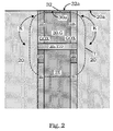
- the tungsten surface area 30a is nitridized so that a nitridized tungsten surface layer 32 covers the tungsten section 30 as an protection layer.
- a high temperature processing step can be performed on the arrangement shown in Fig. 2, avoiding in the high temperature region an oxidation process with respect to adsorbed oxygen molecules on the tungsten surface area 30a as said adsorbed oxygen molecules are replaced or displaced.
- the surface area 32a of the nitridized tungsten layer 32 is still essentially planar so that when coating the arrangement of Fig. 2 with an silicon nitride hard mask layer 40 the surface area 40a of the latter remains planar, in contrast to prior art methods, in which the tungsten whiskers impinge their undulation from the undulated tungsten surface area 40a to the respective surface area 50a of the hard mask layer 40.
Landscapes
- Engineering & Computer Science (AREA)
- Manufacturing & Machinery (AREA)
- Insulated Gate Type Field-Effect Transistor (AREA)
- Electrodes Of Semiconductors (AREA)
Abstract
Description
- LPCVD: at high pressure (> 1 Torr), Tn >= 600°C, time >= 30 min
- PECVD: at high power (∼ 500 W for high ion energy) and time ∼ 30 sec, Tn ∼ 300°C (below W oxidation temperature).
| Example 1: LPCVD SiN deposition at 725°C | |
| process flows: | Pros/Cons: |
| 1 step process: | • Pros: 1 process step in 1 tool |
| • Load in LPCVD furnace at 600°C or lower | |
| • Cons: furnace must be ramp down at low temperature for load in/nitridation → risk of particles | |
| • Thermal nitradation step at this low temperature | |
| • then ramp up at the deposition temperature (725°C) | |
| 2 steps process: | • Pros: no process complexity, short process |
| • Nitradation in PECVD tool | |
| • Load in LPCVD furnace at 700°C | (30 sec), no risk of particles |
| • then ramp up at the deposition temperature (725°C) | • Cons: additional step in different tool |
| Example 1: Annealing in inert ambient at high temperature | |
| process flows: | Pros/Cons: |
| one step process: | • Pros: 1 process step in 1 tool |
| • Load in RTP/furnace at room temperature | |
| • Cons: low temp nitridation require long time | |
| • Thermal nitradation step at low temperature (e.g. 600°C) | |
| • then ramp up at the annealing temperature (e.g. 1050°C) | |
| two steps process: | • Pros: short process (30 sec), additional protection against O2 background |
| • Nitradation in PECVD tool | |
| • Load in RTP/furnace at room temperature | |
| • then ramp up at the annealing temperature (e.g. 1050°C) | • Cons: additional step in different tool |
- Fig. 1 - 3
- are schematical cross-sectional views elucidating intermediate stages with respect to example of an embodiment of the inventive method for processing a semiconductor device.
- 1
- semiconductor device
- 20
- semiconductor section
- 20a
- semiconductor surface area
- 30
- tungsten section
- 30a
- tungsten surface area
- 30b
- sidewall section
- 30c
- bottom section
- 32
- oxidation blocking layer, nitridized tungsten layer
- 32a
- surface area
- 40
- hard mask, silicon nitride
- 40a
- surface area
- 100
- high temperature processing ambient atmosphere
- 102
- intermediate temperature processing ambient atmosphere
- BS
- buried strap region
- G
- gate region, gate section
- GOX
- gate oxide region
- Sh
- shielding
- TE
- top electrode connection
- T
- transistor device
- TTO
- trench top oxide
Claims (12)
- Method for processing a semiconductor device or the like, in particular in a process of manufacturing a DRAM device or the like, comprising the steps of:characterized in thatforming a semiconductor section (20) having at least one semiconductor surface area (20a),forming a tungsten section (30) within said semiconductor section (20) and having a tungsten surface area (30a) being a part of said semiconductor area (20a), andperforming on said semiconductor section (20), said tungsten section (30), and/or the surface areas (20a, 30a) thereof at least one high temperature processing step at a relative high processing temperature (Th) with having at least said tungsten surface area (30a) or a part thereof exposed to an high temperature processing ambient atmosphere (100),before said high temperature processing step an intermediate nitridation processing step is performed at least on said tungsten surface area (30a) at an intermediate processing temperature (Tn) below said high processing temperature (Th), andthereby forming a nitridized tungsten surface layer (32) as an oxidation blocking layer or the like, and/or in particular for avoiding the formation of tungsten whiskers or the like.
- Method according to claim 1, wherein said intermediate nitridation processing step is carried out in an ammonia atmosphere or ammonia containing atmosphere as an intermediate temperature processing ambient atmosphere (102).
- Method according to claim 2, wherein said intermediate temperature processing ambient atmosphere (102) is set at a pressure of about 1 Torr or higher.
- Method according to anyone of the preceding claims, wherein said intermediate processing temperature (Tn) is chosen to be about 500°C or higher.
- Method according to anyone of the preceding claims, wherein said intermediate nitridation processing step is included into or performed during a process of increasing the processing temperature from a relative low processing temperature (Tr), for instance room temperature, to said relative high processing temperature (Th).
- Method according to anyone of the preceding claims, wherein said high temperature processing step at least comprises a high temperature annealing step for said semiconductor device (1).
- Method according to anyone of the preceding claims, wherein said high temperature processing step at least comprises a step of coating at least said semiconductor surface area (20a) with hard mask (40) or spacer elements, in particular using silicon nitride Si3N4 or the like.
- Method according to anyone of the preceding claims, wherein said high temperature processing step at least involves a LPCVD and/or PECVD process or the like.
- Method according to anyone of the preceding claims, wherein the high processing temperature (Th) is set to be about 700°C or higher.
- Method according to anyone of the preceding claims, wherein said intermediate nitridation processing step is performed at an intermediate processing temperature (Tn) of about 600°C as a thermal nitridation processing step.
- Method according to anyone of the claims 1 to 9, wherein said intermediate nitridation processing step is performed at an intermediate processing temperature (Tn) below a tungsten oxidation temperature of about 450°C and in particular at a temperature of about 300°C, in particular using a PECVD method or the like and/or with an energy and/or a back bias of about 500 W.
- Method according to anyone of the preceding claims, wherein said tungsten section (30) is formed as a gate section (G) of a MOSFET arrangement or the like, in particular of a cell selection transistor (T) for a DRAM device (1) or the like.
Priority Applications (1)
| Application Number | Priority Date | Filing Date | Title |
|---|---|---|---|
| EP01121475A EP1298710A1 (en) | 2001-09-07 | 2001-09-07 | Method for protecting a tungsten element in semiconductor device fabrication |
Applications Claiming Priority (1)
| Application Number | Priority Date | Filing Date | Title |
|---|---|---|---|
| EP01121475A EP1298710A1 (en) | 2001-09-07 | 2001-09-07 | Method for protecting a tungsten element in semiconductor device fabrication |
Publications (1)
| Publication Number | Publication Date |
|---|---|
| EP1298710A1 true EP1298710A1 (en) | 2003-04-02 |
Family
ID=8178579
Family Applications (1)
| Application Number | Title | Priority Date | Filing Date |
|---|---|---|---|
| EP01121475A Withdrawn EP1298710A1 (en) | 2001-09-07 | 2001-09-07 | Method for protecting a tungsten element in semiconductor device fabrication |
Country Status (1)
| Country | Link |
|---|---|
| EP (1) | EP1298710A1 (en) |
Citations (4)
| Publication number | Priority date | Publication date | Assignee | Title |
|---|---|---|---|---|
| JPH0277162A (en) * | 1988-06-03 | 1990-03-16 | Sharp Corp | Manufacture of semiconductor device |
| JPH02177427A (en) * | 1988-12-28 | 1990-07-10 | Fujitsu Ltd | Manufacture of semiconductor device |
| US5034787A (en) * | 1990-06-28 | 1991-07-23 | International Business Machines Corporation | Structure and fabrication method for a double trench memory cell device |
| US6284634B1 (en) * | 1999-02-22 | 2001-09-04 | Hyundai Electronics Industries Co., Ltd. | Method for forming metal line in semiconductor device |
-
2001
- 2001-09-07 EP EP01121475A patent/EP1298710A1/en not_active Withdrawn
Patent Citations (4)
| Publication number | Priority date | Publication date | Assignee | Title |
|---|---|---|---|---|
| JPH0277162A (en) * | 1988-06-03 | 1990-03-16 | Sharp Corp | Manufacture of semiconductor device |
| JPH02177427A (en) * | 1988-12-28 | 1990-07-10 | Fujitsu Ltd | Manufacture of semiconductor device |
| US5034787A (en) * | 1990-06-28 | 1991-07-23 | International Business Machines Corporation | Structure and fabrication method for a double trench memory cell device |
| US6284634B1 (en) * | 1999-02-22 | 2001-09-04 | Hyundai Electronics Industries Co., Ltd. | Method for forming metal line in semiconductor device |
Non-Patent Citations (3)
| Title |
|---|
| "SELECTIVE TUNGSTEN NITRIDE FORMATION", IBM TECHNICAL DISCLOSURE BULLETIN, IBM CORP. NEW YORK, US, vol. 31, no. 2, 1 July 1988 (1988-07-01), pages 366 - 368, XP000097132, ISSN: 0018-8689 * |
| PATENT ABSTRACTS OF JAPAN vol. 014, no. 257 (E - 0936) 4 June 1990 (1990-06-04) * |
| PATENT ABSTRACTS OF JAPAN vol. 014, no. 448 (E - 0983) 26 September 1990 (1990-09-26) * |
Similar Documents
| Publication | Publication Date | Title |
|---|---|---|
| US6245616B1 (en) | Method of forming oxynitride gate dielectric | |
| US6638876B2 (en) | Method of forming dielectric films | |
| USRE38674E1 (en) | Process for forming a thin oxide layer | |
| US7271092B2 (en) | Boron incorporated diffusion barrier material | |
| US5891809A (en) | Manufacturable dielectric formed using multiple oxidation and anneal steps | |
| US7429540B2 (en) | Silicon oxynitride gate dielectric formation using multiple annealing steps | |
| US5926741A (en) | Method of forming gate dielectric films for MOSFETs without generation of natural oxide films | |
| US7429538B2 (en) | Manufacturing method for two-step post nitridation annealing of plasma nitrided gate dielectric | |
| US8450221B2 (en) | Method of forming MOS transistors including SiON gate dielectric with enhanced nitrogen concentration at its sidewalls | |
| KR20050096181A (en) | Tailoring nitrogen profile in silicon oxynitride using rapid thermal annealing with ammonia under ultra-low pressure | |
| US5637528A (en) | Semiconductor device manufacturing method including dry oxidation | |
| US20080132086A1 (en) | Reducing nitrogen concentration with in-situ steam generation | |
| JP3399413B2 (en) | Oxynitride film and method for forming the same | |
| EP1298710A1 (en) | Method for protecting a tungsten element in semiconductor device fabrication | |
| JP4999265B2 (en) | Method for manufacturing gate insulating film | |
| JPH10125617A (en) | Method for manufacturing semiconductor device | |
| US20070010103A1 (en) | Nitric oxide reoxidation for improved gate leakage reduction of sion gate dielectrics | |
| JP2002134747A (en) | Low temperature process for hot carrier aging mitigation | |
| KR100351982B1 (en) | Manufacturing method for insulator flim on semiconductor device | |
| KR100914292B1 (en) | Method for forming charge trap layer having silicon nanocrystal, nonvolatile memory device using same and manufacturing method therefor | |
| KR19980050130A (en) | Method of forming gate insulating film of semiconductor device |
Legal Events
| Date | Code | Title | Description |
|---|---|---|---|
| PUAI | Public reference made under article 153(3) epc to a published international application that has entered the european phase |
Free format text: ORIGINAL CODE: 0009012 |
|
| AK | Designated contracting states |
Kind code of ref document: A1 Designated state(s): AT BE CH CY DE DK ES FI FR GB GR IE IT LI LU MC NL PT SE TR Designated state(s): AT BE CH CY DE DK ES FI FR GB GR IE IT LI LU MC NL PT SE TR |
|
| AX | Request for extension of the european patent |
Extension state: AL LT LV MK RO SI |
|
| AKX | Designation fees paid | ||
| REG | Reference to a national code |
Ref country code: DE Ref legal event code: 8566 |
|
| STAA | Information on the status of an ep patent application or granted ep patent |
Free format text: STATUS: THE APPLICATION IS DEEMED TO BE WITHDRAWN |
|
| 18D | Application deemed to be withdrawn |
Effective date: 20031003 |