EP1296544A1 - Flexible printed circuit board and foldable cell phone terminal - Google Patents
Flexible printed circuit board and foldable cell phone terminal Download PDFInfo
- Publication number
- EP1296544A1 EP1296544A1 EP01936845A EP01936845A EP1296544A1 EP 1296544 A1 EP1296544 A1 EP 1296544A1 EP 01936845 A EP01936845 A EP 01936845A EP 01936845 A EP01936845 A EP 01936845A EP 1296544 A1 EP1296544 A1 EP 1296544A1
- Authority
- EP
- European Patent Office
- Prior art keywords
- printed circuit
- circuit board
- flexible printed
- folded
- conductor
- Prior art date
- Legal status (The legal status is an assumption and is not a legal conclusion. Google has not performed a legal analysis and makes no representation as to the accuracy of the status listed.)
- Granted
Links
Images


Classifications
-
- H—ELECTRICITY
- H04—ELECTRIC COMMUNICATION TECHNIQUE
- H04M—TELEPHONIC COMMUNICATION
- H04M1/00—Substation equipment, e.g. for use by subscribers
- H04M1/02—Constructional features of telephone sets
- H04M1/0202—Portable telephone sets, e.g. cordless phones, mobile phones or bar type handsets
- H04M1/0206—Portable telephones comprising a plurality of mechanically joined movable body parts, e.g. hinged housings
- H04M1/0208—Portable telephones comprising a plurality of mechanically joined movable body parts, e.g. hinged housings characterized by the relative motions of the body parts
- H04M1/0214—Foldable telephones, i.e. with body parts pivoting to an open position around an axis parallel to the plane they define in closed position
- H04M1/0216—Foldable in one direction, i.e. using a one degree of freedom hinge
-
- H—ELECTRICITY
- H05—ELECTRIC TECHNIQUES NOT OTHERWISE PROVIDED FOR
- H05K—PRINTED CIRCUITS; CASINGS OR CONSTRUCTIONAL DETAILS OF ELECTRIC APPARATUS; MANUFACTURE OF ASSEMBLAGES OF ELECTRICAL COMPONENTS
- H05K1/00—Printed circuits
- H05K1/02—Details
- H05K1/0277—Bendability or stretchability details
- H05K1/028—Bending or folding regions of flexible printed circuits
-
- H—ELECTRICITY
- H04—ELECTRIC COMMUNICATION TECHNIQUE
- H04M—TELEPHONIC COMMUNICATION
- H04M1/00—Substation equipment, e.g. for use by subscribers
- H04M1/72—Mobile telephones; Cordless telephones, i.e. devices for establishing wireless links to base stations without route selection
- H04M1/725—Cordless telephones
-
- H—ELECTRICITY
- H05—ELECTRIC TECHNIQUES NOT OTHERWISE PROVIDED FOR
- H05K—PRINTED CIRCUITS; CASINGS OR CONSTRUCTIONAL DETAILS OF ELECTRIC APPARATUS; MANUFACTURE OF ASSEMBLAGES OF ELECTRICAL COMPONENTS
- H05K1/00—Printed circuits
- H05K1/02—Details
- H05K1/0213—Electrical arrangements not otherwise provided for
- H05K1/0216—Reduction of cross-talk, noise or electromagnetic interference
- H05K1/0218—Reduction of cross-talk, noise or electromagnetic interference by printed shielding conductors, ground planes or power plane
-
- H—ELECTRICITY
- H05—ELECTRIC TECHNIQUES NOT OTHERWISE PROVIDED FOR
- H05K—PRINTED CIRCUITS; CASINGS OR CONSTRUCTIONAL DETAILS OF ELECTRIC APPARATUS; MANUFACTURE OF ASSEMBLAGES OF ELECTRICAL COMPONENTS
- H05K2201/00—Indexing scheme relating to printed circuits covered by H05K1/00
- H05K2201/05—Flexible printed circuits [FPCs]
- H05K2201/055—Folded back on itself
-
- H—ELECTRICITY
- H05—ELECTRIC TECHNIQUES NOT OTHERWISE PROVIDED FOR
- H05K—PRINTED CIRCUITS; CASINGS OR CONSTRUCTIONAL DETAILS OF ELECTRIC APPARATUS; MANUFACTURE OF ASSEMBLAGES OF ELECTRICAL COMPONENTS
- H05K2201/00—Indexing scheme relating to printed circuits covered by H05K1/00
- H05K2201/20—Details of printed circuits not provided for in H05K2201/01 - H05K2201/10
- H05K2201/2027—Guiding means, e.g. for guiding flexible circuits
Definitions
- the present invention relates to a flexible printed circuit board of which a portion is bent, and relates also to a folding-type cellular telephone terminal having a flexible printed circuit board of which a portion is bent.
- a folding-type (collapsible) cellular telephone terminal such as a folding-type cellular phone or a folding-type PHS (personal handyphone system) phone, has two body casings coupled together with a hinge portion.
- Printed circuit boards having electronic components mounted thereon are housed inside the individual body casings, and are connected together with a flexible printed circuit board.
- the flexible printed circuit board is required to have a sufficiently small width.
- the flexible printed circuit board arranged in the hinge portion is wound in a helical shape.
- the flexible printed circuit board is required to have a smaller width.
- a device such as a folding-type cellular telephone terminal, that employs digital circuits and thus uses a clock pulse, tends to emit pulse noise, making the device a noise source.
- Noise is propagated either by being radiated through the air or by being conducted by a power or signal line.
- wiring is achieved by the use of a flexible printed circuit board
- noise is propagated, by being conducted by the flexible printed circuit board, to other printed circuit boards having electronic components mounted thereon.
- the flexible printed circuit board itself may act as an antenna, receiving noise being radiated through the air and propagating it to the other circuit boards. Such noise can be suppressed by shielding the flexible printed circuit board, but it is not easy to shield it, since it is bent frequently.
- a flexible printed circuit board is provided with first and second insulating sheets, a conductor pattern formed between the first and second insulating sheets, and a shielding conductor fixed to the second insulating sheet.
- the flexible printed circuit board is folded up with the second insulating sheet outside so that the conductor pattern is enclosed inside the shielding conductor.
- a flexible printed circuit board is provided with first and second connection portions where contacts are exposed and first and second path portions where conductor patterns are arranged that connect the contacts of the first and second connection portions together.
- the first and second path portions are formed so as to have substantially symmetrical shapes with each other about a predetermined straight line, and the flexible printed circuit board is folded up along the straight line.
- a folding-type cellular telephone terminal is provided with: first and second body casings; a hinge portion that pivotably couples the first and second body casings together; and a flexible printed circuit board provided with first and second insulating sheets, a conductor pattern formed between the first and second insulating sheets, and a shielding conductor fixed to the second insulating sheet.
- the flexible printed circuit board is arranged so as to bridge between the first and second body casings.
- the flexible printed circuit board is folded up with the second insulating sheet outside so that the conductor pattern is enclosed inside the shielding conductor.
- a folding-type cellular telephone terminal is provided with: first and second body casings; a hinge portion that pivotably couples the first and second body casings together; and a flexible printed circuit board provided with first and second connection portions where contacts are exposed and first and second path portions where conductor patterns are arranged that connect the contacts of the first and second connection portions together.
- the first and second path portions are formed so as to have substantially symmetrical shapes with each other about a predetermined straight line, and the flexible printed circuit board is folded up along the straight line.
- the overlapping portion of the flexible printed circuit board which is formed as a result of the flexible printed circuit board being folded up is arranged so as to form a helical shape in the hinge portion.
- the straight line along which the flexible printed circuit board is folded up is arranged outside the hinge portion, and displacement preventing means for preventing displacement along the straight line is provided only at one end of the first and second path portions.
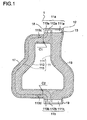
- Figs. 1 and 2 are plan views of a flexible printed circuit board embodying the invention, respectively before and after being shielded. As will be described in detail later, the flexible printed circuit board of this embodiment is incorporated in a folding-type cellular telephone terminal (see Fig. 7),.
- the flexible printed circuit board 1 has a first and a second connection portion 18 and 19 where contact portions 11a and 11b of conductor patterns 11 are exposed.
- the conductor patterns 11 include a first and a second pattern 111 and 112 for signal transmission and a third pattern 113 for grounding.
- the first and second connection portions 18 and 19 are connected together by a first path portion 16 where the first pattern 111 is arranged and a second path potion 17 that branches off the first path portion 18 and where the second and third patterns 111 and 112 are arranged.
- the conductor pattern 11 is vacuum-deposited on a first insulating sheet 12, and on the conductor pattern 11 is laid a second insulating sheet 13 (indicated by hatches ascending rightward in the figures).
- the first and second insulating sheets 12 and 13 are formed of polyimide or polyester about 12.5 ⁇ m (1/2 microinches) thick.
- the conductor pattern 11 is formed of silver or the like about 40 ⁇ m thick.
- the second insulating sheet 13 is laid over the conductor pattern 11 in such a way that individual contact portions 111a, 112a, 113a, 111b, 112b, and 113b of the conductor pattern 11 are exposed. Grounding portions 113c and 113d of the third pattern 113 are also exposed.
- a shielding conductor 14 (indicated by hatches descending rightward in the figures) formed of aluminum or the like is vacuum-deposited.
- the grounding portions 113c and 113d conduct to the shielding conductor 14, which in turn is grounded by way of the third pattern 113.
- substantially central portions of the first and second path portions 16 and 17, as viewed vertically in the figures, are arranged so as to form a helical shape. For this reason, the grounding portions 113c and 113d are formed near the first and second connection portions 18 and 19, where the bending of the first and second path portions 16 and 17 has less effect.
- the external shapes of the first and second path portions 16 and 17 are so designed as to be symmetrical with each other about folding lines C1 and C2 that Lie on a straight line.
- the folding lines C1 and C2 are located away from the first and second connection portions 18 and 19. This permits the first and second connection portions 18 and 19 to be connected to connectors 2a and 3a (see Fig.6) without being bent.
- Fig. 3 is a plan view showing the back side of the flexible printed circuit board 1.
- an adhesive member (displacement preventing means) formed of double-sided adhesive tape or the like is affixed to the first insulating sheets.
- Figs. 4 and 5 are a plan view and a side view, respectively, of the flexible printed circuit board 1 in its state folded up along the folding lines C1 and C2.
- the flexible printed circuit board 1 is folded up along the folding lines C1 and C2 with the adhesive member 15 (see Fig. 3) inside and the shielding conductor 14 (indicated by the rightward descending hatches) outside.
- portions of the first and second path portions 16 and 17 near the second connection portion 19 are bonded together, which prevents the first and second path portions 16 and 17, now facing each other, from being displaced in the direction (indicated by arrows D) perpendicular to the folding lines C1 and C2, and which also prevents the flexible printed circuit board 1, now folded up, from unfolding.
- the first and second path portions 16 and 17 overlap with each other substantially completely, and thus the first pattern 111 now faces the second and the third patterns 112 and 113. That is, the first, second, and third patterns 111, 112, and 113 are now enclosed in the shielding conductor 14 arranged outside.
- the conductor pattern 11 overlaps with itself.
- the conductor pattern 11 does not necessarily have to overlap with itself, as long as the conductor pattern 11 is enclosed in the shielding conductor 14 when the insulating sheet 12 having the shielding conductor 14 fixed thereto is folded up.
- the insulating sheet 13 is formed so as to cover a wider area than where the first and second path portions 16 and 17, facing each other, overlap with each other. This prevents short-circuiting between the first pattern 111 and the second and third patterns 112 and 113.
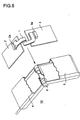
- Fig. 6 is a partially cutaway perspective view of the flexible printed circuit board 1, in its state before being incorporated into a folding-type cellular. telephone terminal.
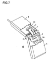
- Fig. 7 is a partially cutaway perspective view of the folding-type cellular telephone terminal having the flexible printed circuit board 1 incorporated therein.
- the folding-type cellular telephone terminal 10 in which the flexible printed circuit board 1 is incorporated is provided with an ear-piece portion (first body casing) 4, a mouth-piece portion (second body casing ) 5, and a hinge portion 6 that pivotably couples the ear-piece portion 4 and the mouth-piece portion 5 together.
- ear-piece portion first body casing
- mouth-piece portion second body casing
- hinge portion 6 that pivotably couples the ear-piece portion 4 and the mouth-piece portion 5 together.
- printed circuit boards 2 and 3 having electronic components mounted thereon.
- the flexible printed circuit board 1 is connected to a connector 2a on the printed circuit board 2 and to a connector 3a on the printed circuit board 3, with a central portion of the flexible printed circuit board 1 bent one turn so as to form a helical shape.
- the flexible printed circuit board 1 is housed in the folding-type cellular telephone terminal 10 with the helical portion (bent portion) of the former placed inside the hinge portion 6 of the latter. Bending the flexible printed circuit board 1 one turn inside the hinge portion 6 helps enhance the durability of the folding-type cellular telephone terminal 10 against its folding and unfolding.
- the flexible printed circuit board 1 is so designed as to be substantially symmetrical about a line, when it is folded up, the first and second path portions 16 and 17 overlap with each other substantially completely. This helps reduce the width of the central portion, as viewed vertically in Fig. 4 described earlier, of the flexible printed circuit board 1 after being folded up. This makes the central portion of the flexible printed circuit board 1, even though it is formed into a helical shape, easy to put in the hinge portion 6. Thus, even if the flexible printed circuit board 1 have more conductor patterns laid thereon, it can easily be housed in the folding-type cellular telephone terminal 10.
- the folding lines C1 and C2 are located outside the hinge portion 6 so as not to run through the helical portion inside the hinge portion 6. This permits the outside and inside of the flexible printed circuit board 1 to move relative to each other in the helical portion thereof placed inside the hinge portion 6.
- the adhesive member 15 is provided only near the second connection portion 19, as the folding-type cellular telephone terminal 10 is unfolded and folded, the second path portion 17 moves relatively toward the first connection portion. This makes it possible to absorb the tensile force resulting from the difference between the external and internal diameters of the helical portion when the folding-type cellular telephone terminal is unfolded and folded. In this way, it is possible to prevent damage to the flexible printed circuit board 1 resulting from a tensile force.
- the flexible printed circuit board 1 of this embodiment has the conductor 11 pattern formed on one side only. However, it is also possible to use a flexible printed circuit board having conductor patterns formed on both sides.
- a flexible printed circuit board has a conductor pattern laid between a first and a second insulating sheet, and is folded up with the second insulating sheet, having a shielding conductor fixed thereto, outside so that the conductor pattern is enclosed in the shielding conductor.
- a shielding conductor fixed thereto, outside so that the conductor pattern is enclosed in the shielding conductor.
- a flexible printed circuit board has a first and a second path portions thereof so designed as to have substantially symmetrical external shapes about a predetermined straight line, and is folded up along this straight line. This permits the first and second path portions to overlap with each other when the flexible printed circuit board is folded up, and thus helps reduce the width of part of the flexible printed circuit board after being folded up.
- the helical portion can easily be put in the hinge portion of a folding-type cellular telephone terminal.
- a flexible printed circuit board is formed into a helical shape in a hinge portion, a folding line is located outside the hinge portion, and a displacement preventing means for preventing displacement in the direction perpendicular to the folding line is provided only at one end of a first and a second path portion.
- This permits the outside and inside of the flexible printed circuit board to move relative to each other inside the hinge portion, and also permits one of the first and second path portions to move relatively at the other end when a folding-type cellular telephone terminal is unfolded and folded.
- This makes it possible to absorb the tensile force resulting from the difference between the external and internal diameters of the helical portion when the folding-type cellular telephone terminal is unfolded and folded. In this way, it is possible to prevent damage to the flexible printed circuit board resulting from a tensile force.
Landscapes
- Engineering & Computer Science (AREA)
- Microelectronics & Electronic Packaging (AREA)
- Signal Processing (AREA)
- Telephone Set Structure (AREA)
- Structure Of Printed Boards (AREA)
- Combinations Of Printed Boards (AREA)
Abstract
Description
Claims (5)
- A flexible printed circuit board comprising first and second insulating sheets, a conductor pattern formed between the first and second insulating sheets, and a shielding conductor fixed to the second insulating sheet, wherein the flexible printed circuit board is folded up with the second insulating sheet outside so that the conductor pattern is enclosed inside the shielding conductor.
- A flexible printed circuit board comprising first and second connection portions where contacts are exposed and first and second path portions where conductor patterns are arranged that connect the contacts of the first and second connection portions together, wherein the first and second path portions are formed so as to have substantially symmetrical shapes with each other about a predetermined straight line, and the flexible printed circuit board is folded up along the straight line.
- A folding-type cellular telephone terminal comprising:wherein the flexible printed circuit board is folded up with the second insulating sheet outside so that the conductor pattern is enclosed inside the shielding conductor.first and second body casings;a hinge portion that pivotably couples the first and second body casings together; anda flexible printed circuit board comprising first and second insulating sheets, a conductor pattern formed between the first and second insulating sheets, and a shielding conductor fixed to the second insulating sheet, the flexible printed circuit board, being arranged so as to bridge between the first and second body casings,
- A folding-type cellular telephone terminal comprising:wherein an overlapping portion of the flexible printed circuit board which is formed as a result of the flexible printed circuit board being folded up is arranged so as to form a helical shape in the hinge portion.first and second body casings;a hinge portion that pivotably couples the first and second body casings together; anda flexible printed circuit board comprising first and second connection portions where contacts are exposed and first and second path portions where conductor patterns are arranged that connect the contacts of the first and second connection portions together, the first and second path portions being formed so as to have substantially symmetrical shapes with each other about a predetermined straight line, the flexible printed circuit board being folded up along the straight line,
- A folding-type cellular telephone terminal as claimed in claim 4,
wherein the straight line along which the flexible printed circuit board is folded up is arranged outside the hinge portion, and displacement preventing means for preventing displacement along the straight line is provided only at one end of the first and second path portions.
Applications Claiming Priority (7)
| Application Number | Priority Date | Filing Date | Title |
|---|---|---|---|
| JP2000198502A JP3515490B2 (en) | 2000-06-30 | 2000-06-30 | Flexible printed circuit board and foldable mobile phone terminal having flexible printed circuit board |
| JP2000198502 | 2000-06-30 | ||
| JP2000333024A JP3773782B2 (en) | 2000-10-31 | 2000-10-31 | Folding mobile phone terminal |
| JP2000333024 | 2000-10-31 | ||
| JP2000333026 | 2000-10-31 | ||
| JP2000333026A JP2002141618A (en) | 2000-10-31 | 2000-10-31 | Flexible printed board and folding portable telephone terminal comprising it |
| PCT/JP2001/004710 WO2002003764A1 (en) | 2000-06-30 | 2001-06-04 | Flexible printed circuit board and foldable cell phone terminal |
Publications (3)
| Publication Number | Publication Date |
|---|---|
| EP1296544A1 true EP1296544A1 (en) | 2003-03-26 |
| EP1296544A4 EP1296544A4 (en) | 2005-08-03 |
| EP1296544B1 EP1296544B1 (en) | 2011-08-03 |
Family
ID=27343927
Family Applications (1)
| Application Number | Title | Priority Date | Filing Date |
|---|---|---|---|
| EP01936845A Expired - Lifetime EP1296544B1 (en) | 2000-06-30 | 2001-06-04 | Flexible printed circuit board and foldable cell phone terminal |
Country Status (3)
| Country | Link |
|---|---|
| US (1) | US6990355B2 (en) |
| EP (1) | EP1296544B1 (en) |
| WO (1) | WO2002003764A1 (en) |
Families Citing this family (35)
| Publication number | Priority date | Publication date | Assignee | Title |
|---|---|---|---|---|
| JP3750587B2 (en) * | 2001-11-05 | 2006-03-01 | 日本電気株式会社 | Foldable mobile phone |
| US6822878B2 (en) | 2002-10-09 | 2004-11-23 | Hewlett-Packard Development Company, L.P. | Circuit board support arrangement, method, and method for using the same |
| ATE370447T1 (en) * | 2002-11-21 | 2007-09-15 | Sony Ericsson Mobile Comm Ab | FLEXIBLE CONDUCTORS SWITCHED BETWEEN TWO PARTS OF A PORTABLE ELECTRONIC DEVICE |
| WO2004046900A2 (en) * | 2002-11-21 | 2004-06-03 | Sony Ericsson Mobile Communications Ab | Flexible conductors connected between two parts of a portable electronic device |
| JP2004266238A (en) * | 2003-01-09 | 2004-09-24 | Sony Chem Corp | Composite wiring board and substrate element piece |
| EP1501202B1 (en) * | 2003-07-23 | 2012-03-28 | LG Electronics, Inc. | Internal antenna and mobile terminal having the internal antenna |
| US7531752B2 (en) * | 2003-07-24 | 2009-05-12 | Nec Corporation | Flexible substrate and electronic device |
| JP4319507B2 (en) * | 2003-10-07 | 2009-08-26 | 京セラ株式会社 | Portable electronic devices |
| US7352592B2 (en) * | 2004-05-21 | 2008-04-01 | Cardiac Pacemakers, Inc. | Method and apparatus for carrying circuit assemblies |
| JP2006073683A (en) * | 2004-08-31 | 2006-03-16 | Sony Corp | CIRCUIT DEVICE AND CIRCUIT DEVICE MANUFACTURING METHOD |
| JP4552565B2 (en) * | 2004-09-03 | 2010-09-29 | 日本電気株式会社 | Flexible wiring board and folding electronic device |
| JP4507789B2 (en) * | 2004-09-21 | 2010-07-21 | 日本電気株式会社 | Stacking connector fixing structure, electronic equipment |
| JP4786197B2 (en) * | 2005-02-25 | 2011-10-05 | 京セラ株式会社 | Portable wireless device |
| US7483727B2 (en) * | 2005-04-04 | 2009-01-27 | Research In Motion Limited | Mobile wireless communications device having improved antenna impedance match and antenna gain from RF energy |
| KR100677475B1 (en) * | 2005-07-14 | 2007-02-02 | 엘지전자 주식회사 | Camera FPC Installation Structure and Installation Method of Portable Terminal |
| KR100659826B1 (en) * | 2005-12-20 | 2006-12-19 | 삼성에스디아이 주식회사 | Circuit board of battery pack |
| KR100744143B1 (en) * | 2006-07-27 | 2007-08-01 | 삼성전자주식회사 | Film wiring board and semiconductor chip package and flat panel display device using same |
| JP5192668B2 (en) * | 2006-07-28 | 2013-05-08 | シャープ株式会社 | Portable terminal |
| JP2008187154A (en) | 2007-01-31 | 2008-08-14 | Nitto Denko Corp | Flexible printed circuit board connection structure and electronic device |
| JP4886603B2 (en) * | 2007-05-31 | 2012-02-29 | 日東電工株式会社 | Printed wiring board |
| US8851356B1 (en) * | 2008-02-14 | 2014-10-07 | Metrospec Technology, L.L.C. | Flexible circuit board interconnection and methods |
| US11266014B2 (en) | 2008-02-14 | 2022-03-01 | Metrospec Technology, L.L.C. | LED lighting systems and method |
| JP4829263B2 (en) * | 2008-02-25 | 2011-12-07 | 富士通株式会社 | Waterproof electronic equipment |
| JP5140028B2 (en) * | 2009-03-26 | 2013-02-06 | 日東電工株式会社 | Wiring circuit board and manufacturing method thereof |
| DE112010005219T5 (en) * | 2010-02-03 | 2012-11-08 | Laird Technologies Ab | A signal transmission device and a portable radio communication device having such a signal transmission device |
| JP5488024B2 (en) * | 2010-02-17 | 2014-05-14 | ミツミ電機株式会社 | AC adapter |
| US20120214556A1 (en) * | 2011-02-17 | 2012-08-23 | Nokia Corporation | Method and Apparatus for Solar Cell Light Concentrator Panel |
| EP2801498A1 (en) | 2013-05-07 | 2014-11-12 | Brusa Elektronik AG | Assembly and method for inductively charging mobile devices |
| KR102340738B1 (en) * | 2014-09-02 | 2021-12-17 | 삼성디스플레이 주식회사 | Curved display apparatus |
| FR3037693B1 (en) * | 2015-06-16 | 2018-07-13 | Ingenico Group | CONTACTLESS COMMUNICATION ANTENNA FOR TERMINAL PAYMENT |
| JP2017146355A (en) * | 2016-02-15 | 2017-08-24 | 船井電機株式会社 | Display device |
| WO2020090157A1 (en) | 2018-11-02 | 2020-05-07 | 株式会社村田製作所 | Flexible wiring board |
| KR102524236B1 (en) * | 2018-11-16 | 2023-04-24 | 삼성전자주식회사 | Electric device including waterproof structure |
| KR102758032B1 (en) * | 2019-08-02 | 2025-01-21 | 삼성전자주식회사 | An electronic device comprising a fpcb |
| JP7483354B2 (en) * | 2019-11-27 | 2024-05-15 | キヤノン株式会社 | Imaging device |
Family Cites Families (16)
| Publication number | Priority date | Publication date | Assignee | Title |
|---|---|---|---|---|
| US3979763A (en) * | 1974-08-05 | 1976-09-07 | Polaroid Corporation | Circuit board arrangement for collapsible camera apparatus |
| JPS53127167U (en) * | 1977-03-17 | 1978-10-09 | ||
| JPS53127167A (en) | 1977-04-12 | 1978-11-07 | Ajinomoto Kk | Method for producing compst from ortanic wastes |
| JPS607516Y2 (en) * | 1978-11-16 | 1985-03-13 | 日本電気株式会社 | Connection structure of small electronic devices |
| JPS5574090A (en) | 1978-11-30 | 1980-06-04 | Matsushita Electric Works Ltd | Device for firing discharge lamp |
| JPS6489845A (en) * | 1987-09-30 | 1989-04-05 | Matsushita Electric Industrial Co Ltd | Electric appliance |
| US5117073A (en) * | 1991-04-02 | 1992-05-26 | Motorola, Inc. | Control signal initiator responsive to a hinge position |
| US5375321A (en) * | 1993-03-30 | 1994-12-27 | United States Department Of Energy | Method for fabricating fan-fold shielded electrical leads |
| JP2522194B2 (en) | 1993-12-30 | 1996-08-07 | ソニー株式会社 | Signal line with shield |
| JP3262151B2 (en) * | 1994-11-24 | 2002-03-04 | 富士写真光機株式会社 | Flexible printed circuit board |
| JP2926212B2 (en) | 1995-09-08 | 1999-07-28 | 日本航空電子工業株式会社 | Hinge connector |
| SG70987A1 (en) * | 1995-05-09 | 2000-03-21 | Motorola Inc | Method and apparatus for routing conductors |
| JPH09153931A (en) * | 1995-11-30 | 1997-06-10 | Mitsubishi Electric Corp | Opening and closing mechanism |
| JPH09199811A (en) | 1996-01-16 | 1997-07-31 | Sumitomo Wiring Syst Ltd | Flexible printed circuit board and manufacture thereof |
| US6421531B1 (en) * | 1997-01-28 | 2002-07-16 | Framatome Connectors International | Mobile telephone with articulated cover and revolving contacts |
| US6352434B1 (en) * | 1997-10-15 | 2002-03-05 | Motorola, Inc. | High density flexible circuit element and communication device using same |
-
2001
- 2001-06-04 EP EP01936845A patent/EP1296544B1/en not_active Expired - Lifetime
- 2001-06-04 WO PCT/JP2001/004710 patent/WO2002003764A1/en not_active Ceased
- 2001-06-04 US US10/069,622 patent/US6990355B2/en not_active Expired - Fee Related
Also Published As
| Publication number | Publication date |
|---|---|
| US6990355B2 (en) | 2006-01-24 |
| WO2002003764A1 (en) | 2002-01-10 |
| EP1296544B1 (en) | 2011-08-03 |
| EP1296544A4 (en) | 2005-08-03 |
| US20020135993A1 (en) | 2002-09-26 |
Similar Documents
| Publication | Publication Date | Title |
|---|---|---|
| US6990355B2 (en) | Flexible printed circuit board and foldable cell phone terminal | |
| EP2046103B1 (en) | Flexible printed board, electronic device equipped with it, and flexible printed board folding method | |
| JP3564053B2 (en) | Flexible cable | |
| EP1501340A2 (en) | Flexible substrate and electronic device | |
| JP2006073840A (en) | Flexible wiring substrate and folding electronic equipment | |
| JP2004088020A (en) | Flexible printed board and electronic device provided with the board | |
| JP2006042102A (en) | Foldable portable radio | |
| CN115207600A (en) | Communication device | |
| JP3992470B2 (en) | Flexible printed circuit board having cable part | |
| US20100079961A1 (en) | Printed circuit board and electronic device | |
| JP4319385B2 (en) | Mobile communication terminal device and flexible substrate | |
| US7359217B2 (en) | Pivoting apparatus with a shielding function | |
| JP2009200015A (en) | Connector for flexible wiring board and electronic device | |
| KR20050040379A (en) | Flexible printed circuit board having bulgy and hollow shape and camera-phone therewith | |
| JP2002141618A (en) | Flexible printed board and folding portable telephone terminal comprising it | |
| KR100678187B1 (en) | Cable connection device between printed circuit board of mobile terminal | |
| JP2006173473A (en) | Cradle for portable information terminal | |
| JP3515490B2 (en) | Flexible printed circuit board and foldable mobile phone terminal having flexible printed circuit board | |
| JP3678113B2 (en) | Printed circuit manufacturing method and portable communication device | |
| JP4642568B2 (en) | Foldable portable electronic device | |
| JP2002111138A (en) | Flexible printed board and electronic apparatus using the same | |
| JP2002141989A (en) | Foldable portable telephone terminal | |
| JP4309230B2 (en) | Portable terminal device and flexible printed wiring board | |
| KR100690780B1 (en) | Mobile communication terminal | |
| JP2013106286A (en) | Electronic apparatus and antenna unit |
Legal Events
| Date | Code | Title | Description |
|---|---|---|---|
| PUAI | Public reference made under article 153(3) epc to a published international application that has entered the european phase |
Free format text: ORIGINAL CODE: 0009012 |
|
| 17P | Request for examination filed |
Effective date: 20020226 |
|
| AK | Designated contracting states |
Kind code of ref document: A1 Designated state(s): AT BE CH CY DE DK ES FI FR GB GR IE IT LI LU MC NL PT SE TR |
|
| RBV | Designated contracting states (corrected) |
Designated state(s): DE FI FR GB SE |
|
| A4 | Supplementary search report drawn up and despatched |
Effective date: 20050617 |
|
| RIC1 | Information provided on ipc code assigned before grant |
Ipc: 7H 05K 5/02 B Ipc: 7H 05K 9/00 B Ipc: 7H 05K 1/00 B Ipc: 7H 05K 7/14 B Ipc: 7H 04M 1/02 B Ipc: 7H 05K 1/02 A Ipc: 7H 05K 7/00 B |
|
| 17Q | First examination report despatched |
Effective date: 20070123 |
|
| RIC1 | Information provided on ipc code assigned before grant |
Ipc: H05K 1/02 20060101ALN20101116BHEP Ipc: H04M 1/725 20060101ALN20101116BHEP Ipc: H05K 1/00 20060101AFI20101116BHEP |
|
| GRAP | Despatch of communication of intention to grant a patent |
Free format text: ORIGINAL CODE: EPIDOSNIGR1 |
|
| GRAS | Grant fee paid |
Free format text: ORIGINAL CODE: EPIDOSNIGR3 |
|
| GRAA | (expected) grant |
Free format text: ORIGINAL CODE: 0009210 |
|
| AK | Designated contracting states |
Kind code of ref document: B1 Designated state(s): DE FI FR GB SE |
|
| REG | Reference to a national code |
Ref country code: GB Ref legal event code: FG4D |
|
| REG | Reference to a national code |
Ref country code: DE Ref legal event code: R096 Ref document number: 60145078 Country of ref document: DE Effective date: 20110929 |
|
| REG | Reference to a national code |
Ref country code: SE Ref legal event code: TRGR |
|
| PLBE | No opposition filed within time limit |
Free format text: ORIGINAL CODE: 0009261 |
|
| STAA | Information on the status of an ep patent application or granted ep patent |
Free format text: STATUS: NO OPPOSITION FILED WITHIN TIME LIMIT |
|
| 26N | No opposition filed |
Effective date: 20120504 |
|
| REG | Reference to a national code |
Ref country code: DE Ref legal event code: R097 Ref document number: 60145078 Country of ref document: DE Effective date: 20120504 |
|
| REG | Reference to a national code |
Ref country code: DE Ref legal event code: R082 Ref document number: 60145078 Country of ref document: DE Representative=s name: GLAWE DELFS MOLL PARTNERSCHAFT MBB VON PATENT-, DE |
|
| REG | Reference to a national code |
Ref country code: GB Ref legal event code: 732E Free format text: REGISTERED BETWEEN 20140807 AND 20140813 |
|
| REG | Reference to a national code |
Ref country code: DE Ref legal event code: R082 Ref document number: 60145078 Country of ref document: DE Effective date: 20140808 Representative=s name: GLAWE DELFS MOLL PARTNERSCHAFT MBB VON PATENT-, DE Ref country code: DE Ref legal event code: R081 Ref document number: 60145078 Country of ref document: DE Owner name: PANASONIC INTELLECTUAL PROPERTY CORPORATION OF, US Free format text: FORMER OWNER: SANYO ELECTRIC CO., LTD., TOTTORI SANYO ELECTRIC CO., LTD, , JP Effective date: 20110808 Ref country code: DE Ref legal event code: R081 Ref document number: 60145078 Country of ref document: DE Owner name: PANASONIC INTELLECTUAL PROPERTY CORPORATION OF, US Free format text: FORMER OWNER: SANYO ELECTRIC CO., LTD., TOTTORI SANYO ELECTRIC CO., LTD, , JP Effective date: 20140808 Ref country code: DE Ref legal event code: R081 Ref document number: 60145078 Country of ref document: DE Owner name: PANASONIC INTELLECTUAL PROPERTY CORPORATION OF, US Free format text: FORMER OWNERS: SANYO ELECTRIC CO., LTD., MORIGUCHI-SHI, OSAKA, JP; TOTTORI SANYO ELECTRIC CO., LTD., TOTTORI, JP Effective date: 20110808 Ref country code: DE Ref legal event code: R081 Ref document number: 60145078 Country of ref document: DE Owner name: PANASONIC INTELLECTUAL PROPERTY CORPORATION OF, US Free format text: FORMER OWNERS: SANYO ELECTRIC CO., LTD., MORIGUCHI-SHI, OSAKA, JP; TOTTORI SANYO ELECTRIC CO., LTD., TOTTORI, JP Effective date: 20140808 |
|
| REG | Reference to a national code |
Ref country code: FR Ref legal event code: TQ Owner name: PANASONIC INTELLECTUAL PROPERTY CORPORATION OF, US Effective date: 20140922 Ref country code: FR Ref legal event code: TQ Owner name: TOTTORI SANYO ELECTRIC CO., LTD., JP Effective date: 20140922 |
|
| REG | Reference to a national code |
Ref country code: FR Ref legal event code: PLFP Year of fee payment: 15 |
|
| PGFP | Annual fee paid to national office [announced via postgrant information from national office to epo] |
Ref country code: SE Payment date: 20150611 Year of fee payment: 15 Ref country code: DE Payment date: 20150527 Year of fee payment: 15 Ref country code: FI Payment date: 20150609 Year of fee payment: 15 Ref country code: GB Payment date: 20150603 Year of fee payment: 15 |
|
| PGFP | Annual fee paid to national office [announced via postgrant information from national office to epo] |
Ref country code: FR Payment date: 20150608 Year of fee payment: 15 |
|
| REG | Reference to a national code |
Ref country code: DE Ref legal event code: R082 Ref document number: 60145078 Country of ref document: DE |
|
| REG | Reference to a national code |
Ref country code: DE Ref legal event code: R119 Ref document number: 60145078 Country of ref document: DE |
|
| PG25 | Lapsed in a contracting state [announced via postgrant information from national office to epo] |
Ref country code: FI Free format text: LAPSE BECAUSE OF NON-PAYMENT OF DUE FEES Effective date: 20160604 |
|
| REG | Reference to a national code |
Ref country code: SE Ref legal event code: EUG |
|
| PG25 | Lapsed in a contracting state [announced via postgrant information from national office to epo] |
Ref country code: SE Free format text: LAPSE BECAUSE OF NON-PAYMENT OF DUE FEES Effective date: 20160605 |
|
| GBPC | Gb: european patent ceased through non-payment of renewal fee |
Effective date: 20160604 |
|
| REG | Reference to a national code |
Ref country code: FR Ref legal event code: ST Effective date: 20170228 |
|
| PG25 | Lapsed in a contracting state [announced via postgrant information from national office to epo] |
Ref country code: FR Free format text: LAPSE BECAUSE OF NON-PAYMENT OF DUE FEES Effective date: 20160630 Ref country code: DE Free format text: LAPSE BECAUSE OF NON-PAYMENT OF DUE FEES Effective date: 20170103 |
|
| PG25 | Lapsed in a contracting state [announced via postgrant information from national office to epo] |
Ref country code: GB Free format text: LAPSE BECAUSE OF NON-PAYMENT OF DUE FEES Effective date: 20160604 |