Field of the Invention
The invention relates to a CDMA (code-division multiple
access) receiver employing a direct sequence CDMA communication
scheme.
Background Art
A CDMA receiver employing a direct sequence CDMA
communication scheme is equipped with a path searcher for seeking
a despread timing. The path searcher is in turn equipped with
a matched filter or a sliding correlator. In the case where the
matched filter is provided, the matched filter is provided with
a delay device, a multiplier, and an adder.
As a sampling frequency used for sampling a received signal
becomes higher, a despread timing (i.e., a path timing) can be
detected with high accuracy. However, if oversampling is
effected for increasing a sampling frequency, the matched filter
will require delay devices which are equal in number to a multiple
of an oversampling ratio.
To solve this problem, a CDMA receiver described in Japanese
Patent Application Laid-Open No. 82973/2000 is provided with
first and second circuit sections. The first circuit section
is constituted of a matched filter for allowing input of a signal
received through low-speed oversampling, and is used for
detecting a coarse despread timing. The second circuit section
is equipped with an integrator and a matched filter. On the basis
of the coarse despread timing detected by the first circuit section,
a highly accurate despread timing is determined through
high-speed oversampling.
However, in the CDMA receiver described in Japanese Patent
Application Laid-Open No. 82973/2000, the second circuit section
performs processing after the first circuit section has performed
processing. Path search processing involves consumption of
time; consequently, there arises a problem of overall despread
processing consuming a considerable amount of time . Although
the first circuit section can be made compact, a necessity for
use of the second circuit section arises. On the whole, not much
reduction in the size of circuitry is achieved.
The invention aims at providing a CDMA receiver which can
render compact a circuit including a matched filter and diminish
load stemming from despread process.
Disclosure of the Invention
The invention has been conceived to solve the problem.
First, a receiver of CDMA communications scheme comprises a
matched filter which operates at a frequency of one-over-n ("n"
is an integer) times the sampling frequency of a received signal
and detects a path timing; and a finger section for despreading
the received signal, wherein the finger section comprises a DLL
which operates at the sampling frequency of the received signal
and computes a difference value representing an offset between
the received signal and a demodulation timing specified by a
path timing detected by the matched filter; a timing adjustment
section which outputs a timing signal of predetermined cycle
while the path timing detected by the matched filter is taken
as a reference and which compensates for the phase of the timing
signal on the basis of the difference value computed by the DLL;
and a despread section which performs despreading operation at
a demodulation timing specified by the timing signal output from
the timing adjustment section.
In the receiver of the first configuration, the matched
filter operates at a frequency of one-over-n ("n" is an integer)
times the sampling frequency of a received signal and detects
a path timing. The DLL provided in the finger section computes
a difference value representing an offset between the received
signal and a demodulation timing. The timing adjustment section
compensates for the phase of the timing signal on the basis of
the difference value. Specifically, the timing adjustment
section causes the phase of the timing signal to advance or delay
in a predetermined situation; for example, when an absolute value
of the difference value is greater than a predetermined threshold
value. More specifically, when the demodulation timing lags
behind the received signal, the phase of the timing signal is
caused to advance. In contrast, when the demodulation timing
is advanced in relation to the received signal, the phase of
the timing signal is caused to delay. The despread section
performs despreading operation at the demodulation timing
specified by the timing adjustment section.
According to the receiver of the first configuration, the
matched filter operates at a frequency of one-over-n ("n" is
an integer) times the sampling frequency of a received signal,
thereby enabling a reduction in the size of a circuit of the
matched filter. The demodulation timing roughly ascertained by
the matched filter is compensated on the basis of information
output from the DLL. The DLL, which is originally provided in
the CDMA receiver, is utilized, thereby preventing an increase
in the size of a circuit of the receiver and processing load.
A correlation peak position can be detected with an accuracy
of sampling frequency, and hence demodulation operation can be
performed with a superior signal-to-noise ratio.
Second, in relation to the first configuration, the timing
adjustment section compensates for the phase of the timing signal
in a predetermined situation and in accordance with a result
of comparison between the difference value computed by the DLL
and a predetermined threshold value. For instance, when the
magnitude of the difference value is greater than a predetermined
threshold value, the compensation operation is performed.
Third, in relation to the first or second configuration,
the timing adjustment section causes the phase of the timing
signal to advance when the magnitude of the difference value
computed by the DLL exceeds a predetermined threshold value and
when the difference value represents that the demodulation timing
lags behind the received signal, and causes the phase of the
timing signal to delay when the magnitude of the difference value
computed by the DLL exceeds the predetermined threshold value
and when the difference value represents that the demodulation
timing is advanced in relation to the received signal. In this
way, the phase of the timing signal can be compensated.
Fourth, in relation to the first or second configuration,
the timing adjustment section causes the phase of the timing
signal to advance when the difference value computed by the DLL
is positive and exceeds a predetermined threshold value ; and
causes the phase of the timing signal to delay when the difference
value computed by the DLL is negative and less than a second
threshold value, which threshold value corresponds to the
predetermined threshold value when it is made negative.
Fifth, in relation to the first, second, third, or fourth
configuration, the timing adjustment section causes the phase
of the timing signal to advance or delay by an amount corresponding
to one clock cycle or a plurality of clock cycles of sampling
frequency of the received signal when the phase of the timing
signal is compensated.
Sixth, in relation to the first, second, third, fourth,
or fifth configuration, the timing adjustment section first
outputs the timing signal after a predetermined period of time
has lapsed from a path timing detected by a matched filter and
compensates for the phase of the timing signal in accordance
with the difference value computed by the DLL.
Seventh, in relation to the first, second, third, fourth,
fifth, or sixth configuration, the DLL comprises a first generator
for outputting a spreading code on the basis of a timing signal
output from the timing adjustment section; a third generator
for outputting a spreading code while lagging behind the timing
at which the first generator produces an output, by a delay period
corresponding to a period of two chips or less; and a second
generator for outputting a spreading code while lagging behind
half the delay period.
Eighth, in relation to the first, second, third, fourth,
fifth, sixth, or seventh configuration, the receiver further
comprises a conversion section which down-samples the received
signal to a frequency of one-over-n ("n" is an integer) times
the sampling frequency of the received signal and outputs the
down-sampled received signal to the matched filter. As a result,
the received signal that has been subjected to down-sampling
can be sent to the matched filter.
Ninth, a receiving method of CDMA communications scheme,
comprises: a path timing detection step of detecting a path timing
through use of a matched filter which operates at a frequency
of one-over-n ("n" is an integer) times the sampling frequency
of a received signal and detects a path timing; a difference
value computation step of computing a difference value
representing an offset between the received signal and a
demodulation timing specified by a path timing detected in the
path timing detection step, through use of a DLL which operates
at the sampling frequency of the received signal; a timing signal
output process for outputting a timing signal of predetermined
cycle while the path timing detected in the path timing detection
step is taken as a reference; and a compensation step of
compensating for the phase of the timing signal to be output
in the timing signal output process, on the basis of the difference
value computed in the difference value computation step.
Therefore, according to the receiving method of the ninth
configuration, the matched filter is operated at a frequency
of one-over-n ("n" is an integer) times the sampling frequency
of a received signal, thereby enabling a reduction in the size
of a circuit of the matched filter. The demodulation timing
roughly ascertained by the matched filter is compensated on the
basis of information output from the DLL. The DLL, which is
originally provided in the CDMA receiver, is utilized, thereby
preventing an increase in the size of a circuit of the receiver
and processing load. A correlation peak position can be detected
with an accuracy of sampling frequency, and hence demodulation
operation can be performed with a superior signal-to-noise ratio.
Tenth, in relation to the ninth configuration, the phase
of the timing signal is compensated in the compensation step
in a predetermined situation and in accordance with a result
of comparison between the difference value computed in the
difference value computation step and a predetermined threshold
value. For instance, when the magnitude of the difference value
is greater than a predetermined threshold value, the compensation
operation is performed.
Eleventh, in relation to the ninth or tenth configuration,
the phase of the timing signal is caused to advance in the
compensation step when the magnitude of the difference value
computed in the difference value computation step exceeds a
predetermined threshold value and when the difference value
represents that the demodulation timing lags behind the received
signal, and the phase of the timing signal is caused to delay
in the compensation step when the magnitude of the difference
value computed in the difference value computation step exceeds
the predetermined threshold value and when the difference value
represents that the demodulation timing is advanced in relation
to the received signal.
Twelfth, in relation to the ninth or tenth configuration,
the phase of the timing signal is caused to advance in the
compensation step when the difference value computed in the
difference value computation step is positive and exceeds a
predetermined threshold value, and the phase of the timing signal
is caused to delay in the compensation step when the difference
value computed in the difference value computation step is
negative and less than a second threshold value, which threshold
value corresponds to the predetermined threshold value when it
is made negative.
Thirteenth, in relation to the ninth, tenth, eleventh,
or twelfth configuration, the phase of the timing signal is caused
to advance or delay by an amount corresponding to one clock cycle
or a plurality of clock cycles of sampling frequency of the received
signal when the phase of the timing signal is compensated in
the compensation step.
Fourteenth, in relation to the ninth, tenth, eleventh,
twelfth, or thirteenth configuration, the timing signal is first
output in the timing signal output step after a predetermined
period of time has lapsed from a path timing detected in the
path timing detection step, and the phase of the timing signal
is compensated in the compensation step in accordance with the
difference value computed in the compensation step.
Brief Description of the Drawings
Fig. 1 is a block diagram showing the configuration of
a receiver according to an embodiment of the invention; Fig.
2 is a block diagram showing the configuration of a matched filter;
Fig. 3 is a block diagram showing the detailed configuration
of a finger; Fig. 4 is a block diagram showing the configuration
of a spreading code generator; Fig. 5 is a descriptive view showing
the operation of a receiver according to an embodiment of the
invention; Fig. 6 is a descriptive view showing the operation
of a receiver according to the embodiment of the invention; Fig.
7 is a descriptive view showing the operation of a receiver
according to the embodiment of the invention; Fig. 8 is a
descriptive view showing the operation of a receiver according
to the embodiment of the invention; and Fig. 9 is a descriptive
view showing the operation of a receiver according to the
embodiment of the invention.
Best Mode for Implementing the Invention
A preferred embodiment of the invention will be described
hereinbelow by utilization of drawings. As shown in Fig. 1, a
receiver A of the invention comprises a speed conversion section
(conversion section) 10, a matched filter 20, fingers (finger
sections) 30, a RAKE combiner section 90, and a control section
100.
Here, the speed conversion section 10 is a circuit for
subjecting a received signal to down-sampling. For instance,
the speed conversion section converts a received signal which
has been oversampled at a ratio of four times a chip rate to
a received signal oversampled by two times. In other words, the
receiving signal input to the receiver A is a digital signal
obtained as a result of a received signal being oversampled by
four times. The speed conversion section 10 subjects the
thus-input received signal to diminishment processing, thus
producing a received signal oversampled by two times. The speed
conversion section may be called "speed conversion means" or
a "speed converter."
The matched filter 20 determines a correlation value
between a received signal and a spreading code, thereby outputting
a path timing signal indicating a timing (path timing) of a peak
position. As shown in Fig. 2, the matched filter 20 comprises
delay devices 21-1 through 21-n; multipliers 22-1 through 22-n;
an adder 23; a memory device 24; and a control section 25. Received
signals are sequentially input to the delay devices 21-1 through
21-n from the speed conversion section 10. A fixed spreading
code is input to the multipliers 22-1 through 22-n, where the
received signals output from the delay devices 21-1 through 21-n
are subjected to multiplication. Here, the adder 23 adds together
results of multiplication operations performed by the multipliers
22-1 to 22-n. The memory device 24 stores a result of addition
output from the adder 23. Specifically, the result of addition
corresponding to one symbol is stored in the memory 24. The
control section 25 detects a timing of peak position on the basis
of the result of addition stored in the memory device 24 and
outputs a path timing signal representing the timing. The path
timing signal is essentially output on a per-symbol basis.
Alternatively, the signal may be output on a per-symbols basis.
The path timing signal represents time information about
a peak position. Strictly speaking, the path timing signal is
a data set pertaining to time which has lapsed since the matched
filter 20 started operation (the time will be described as a
"relative time") . Specifically, the control section 25 detects
a peak position on the basis of the data stored in the memory
24, computes the relative time of the peak position, and outputs
the relative time data as a path timing signal.
In the embodiment, the received signal that has been sampled
by two times is input into the matched filter 20 from the speed
conversion section 10. The matched filter 20 acts as a matched
filter which performs two-times oversampling.
Here, a peak position to be detected includes a sub-peak.
In other words, timings for a plurality of paths are detected
in consideration of a reflected wave or the like. A path timing
signal for each of the timings is output.
In the above description, a path timing signal to be output
from the matched filter 20 is a time data set pertaining to a
peakposition. However, the matched filter 20 may output directly
to a control section 100 data pertaining to a correlation value
for each timing as a path timing signal. In short, the matched
filter 20 outputs directly to the control section 100 data
pertaining to a correlation value for each timing of two-times
oversampling. As shown in Figs. 5(a) and 5(b), the matched filter
20 computes a correlation value on
per-two-times-oversampling-cyclebasis. The data pertaining to
a correlation value are output to the control section 100. Take,
for instance, a graph shown in Fig. 5 (b) as an example, wherein
data pertaining to a correlation value are output on
per-one-half-chip basis. In this case, a two-times oversampling
cycle corresponds to one-half a chip. Here, the matched filter
20 outputs a signal assuming a waveform such as that shown in
Fig. 5(a). Strictly, as mentioned above, data pertaining to a
correlation value are output on a
per-two-times-oversampling-cycle basis. Fig. 5(b) shows apeak
position in an enlarged manner.
It has been described that there are two cases; namely,
a case the matched filter 20 outputs time data pertaining to
a peak position (this is taken as a "first method"), and a case
where the matched filter 20 outputs data pertaining to a
correlation value in its present form (this is taken as a "second
method"). Conceivable criteria for selecting either the first
or second method are as follows: namely, the first method is
employed when one peak is detected from one symbol, and the second
method is employed when a plurality of peaks are detected from
one symbol.
As mentioned above, an additional statement regarding the
case where the matched filter 20 outputs a signal representing
time data pertaining to a peak position as a path timing signal
is that, for example, time data pertaining to Ta shown in Fig.
5(b) are output when time information about a peak position PK
shown in Fig. 5(a) is output.
Each of the fingers 30 performs a despreading operation
for each path of a received signal. The plurality of fingers
30 are provided so as to correspond to respective paths. Each
of the fingers 30 has a DLL (delay locked loop) 40, a timing
adjustment section 60, and a despread section 80.
In relation to a received signal, the DLL 40 outputs a
difference between a correlation device output pertaining to
a spreading E(Early)-code and a correlation device output
pertaining to a spreading L(Late)-code. The DLL 40 comprises
multipliers 42a, 42a, detectors 44a, 44b, a subtractor 48, and
a loop filter 50. Here, the detector 44a summates signals output
from the multiplier 42a and for each symbol period delivers a
correlation output to the subtractor 48. The detector 44b
summates signals output from the multiplier 42b and for each
symbol period delivers a correlation output to the subtractor
48.
As shown in Fig. 4, a spreading code generator 70 shown
in Fig. 3 has a first generator 72, a second generator 74, and
a third generator 76. The first generator 72 outputs a spreading
code to the multiplier 42a, and the third generator 76 outputs
a spreading code to the multiplier 42b. The first generator 72
and the third generator 76 are constituted in the DLL 40. The
first generator 72 outputs a spreading code which is to serve
as an E-code, and the third generator 76 outputs a spreading
code which is serve as an L-code. The second generator 74 is
constituted of a despread section 80.
The first generator 72, the second generator 74, and the
third generator 76 sequentially output spreading codes with a
delay corresponding to one-half of a chip. As shown in Fig. 7,
the second generator 74 outputs a spreading code at a timing
at which a HOLD signal (which will be described later) output
from the timing adjustment section 60 has become LOW; that is,
at a LOW timing (see Fig. 7(b)). The first generator 72 outputs
a spreading code at a phase which has advanced by one-half a
chip in relation to the LOW timing (see Fig. 7(a)). Further,
the third generator 76 outputs a spreading code at a phase which
lags behind the LOW timing by one-half a chip (see Fig. 7(c)).
Here, the third generator 76 outputs a spreading code while lagging
behind the output timing of the first generator 72 by a period
corresponding to one chip. In this case, the period of one chip
corresponds to a delay time described in claims.
The timing adjustment section 60 outputs a HOLD signal.
As shown in Figs. 6(a) and 6(b), the HOLD signal has a frequency
of a chip rate and becomes LOW at a period of the frequency.
Symbol "fs" shown in Fig. 6 designates a sampling frequency at
a chip rate. Individual circuits (e.g., individual sections of
the fingers 30, the RAKE combiner section 90, or the like) become
operative at a timing at which the HOLD signal has become LOW.
The HOLD signal essentially becomes LOW at every cycle
of the frequency of a chip rate. In a predetermined case, the
phase of a LOW timing is compensated in accordance with a path
timing signal delivered from the matched filter 20 by way of
the control section 100 and a difference value output from the
DLL 40.
When the difference value delivered from the DLL 40
represents a phase advance and when the phase advance has exceeded
a predetermined threshold value, the timing adjustment section
60 performs a control operation for causing the phase of the
LOW timing to delay from a timing indicated by the path timing
signal output from the matched filter 20. In contrast, when the
difference value delivered from the DLL 40 indicates a phase
delay and the phase delay has exceeded a predetermined threshold
value, the timing adjustment section 60 performs a control
operation for causing the phase of the LOW timing to advance
in relation to the timing indicated by the path timing signal
output from the matched filter 20. As mentioned above, when the
difference value has exceeded a predetermined threshold value,
a phase is corrected. Here, a period during which a phase is
caused to advance or delayed is set so as to correspond to one
clock. Here, one clock is one operation clock cycle during which
the fingers 30 are to operate. In short, one clock is based on
a sampling frequency employed for four-times oversampling.
As mentioned above, the HOLD signal essentially becomes
LOW at a predetermined cycle. The HOLD signal; particularly,
a HOLD signal of LOW timing, corresponds to a phrase "timing
signal of predetermined cycle which employs a path timing as
a reference" provided in claims. Specifically, the HOLD signal
corresponds to a "timing signal" in a phrase "a timing adjustment
section which outputs a timing signal of predetermined cycle
while a path timing detected by the matched filter is taken as
a reference." The timing adjustment sectionmay be called "timing
adjustment means" or a "timing adjustment device."
Next, the despread section 80 despreads a received signal.
The despread section 80 has the second generator 74, a multiplier
82, and a detector 84, such as those shown in Figs. 3 and 4.
The despread section 80 performs a despreading operation at a
demodulation timing (i.e., a despread timing) based on the HOLD
signal output from the timing adjustment section 60, and detailed
explanations thereof will be provided later. The despread
section may also be called "despread means" or a "despread device."
The RAKE combiner section 90 is a circuit for combining
a received signal that has been despread by each of the fingers
30. In other words, there is performed processing for bringing
signals of respective paths in phase with each other by means
of compensating for the amount of phase rotation arising in the
respective paths or processing for merging together the signals
of respective paths that have been brought in phase with each
other. The fingers 30 and the RAKE combiner section 90 demodulate
a received signal.
The control section 100 controls operations of individual
sections of a receiver A. In particular, the control section
100 has a function of converting relative time data indicated
by a path timing signal to absolute time data when the path timing
signal has been sent to the control section 100 from the matched
filter 20. Here, the absolute time is a local time retained in
the receiver A or a time (an hour) indicated by a local timer
provided in the receiver A. The absolute time becomes a reference
for the receiver A. The control section 100 sends the timing
of a peak position to the timing adjustment section 60 after
having expressed the timing as an absolute time.
When the matched filter 20 sends data pertaining to a
correlation value in their present form to the control section
100, the control section 100 computes a relative time from the
data pertaining to the correlation value, further computes the
absolute time from the relative time, and sends information about
the thus-computed absolute time to the timing adjustment section
60. Specifically, the control section 100 retains a program which
computes a relative time from the thus-delivered data pertaining
to a correlation value and computes an absolute time from the
relative time. The control section 100 performs an arithmetic
operation in accordance with the program. The control section
100 may be arranged so as to compute an absolute time directly
from the data pertaining to a correlation value delivered from
the matched filter 20.
In Fig. 1, the individual sections enclosed by an area
P; that is, the fingers 30, the RAKE combiner section 90, and
the speed conversion section 10 perform four-times oversampling
operation. The matched filter 20 enclosed by an area Q performs
two-times oversampling operation. Specifically, the individual
sections enclosed by the area P perform four-times oversampling
operations. Further, the matched filter 20 enclosed by the area
Q performs two-times oversampling operation.
Operation of the receiver A having the foregoing
configuration; particularly, a receiving method of CDMA
communication scheme performed by the receiver A, will now be
described. Descriptions provided below are directed toward a
path search operation performed during a receiving operation;
namely, initial synchronization capturing operation.
First, a received signal is input to the receiver A. The
receiving signal has been sampled through over-sampling which
is four times a chip rate and subjected to analog-to-digital
conversion processing.
The speed conversion section 10 performs down-sampling
operation, thereby converting the received signal to a
two-times-oversampled received signal. The
two-times-oversampled received signal is delivered to a matched
filter 20. The matched filter 20 detects a peak position and
outputs timing signals for respective paths; that is, path timing
signals. The path timing signals are sent to the control section
100. The control section 100 sends the path timing signals to
the timing adjustment sections 60 of the fingers 30. The process
for detecting a peak position by use of the matched filter 20
corresponds to a path timing detection process described in
claims.
Strictly, relative time data representing a peak position
are sent as a path timing signal to the control section 100 from
the matched filter 20. The control section 100 sends a path timing
signal expressed as a relative time to the timing adjustment
section 60 after the path timing signal has been converted to
an absolute time. Here, the signal to be sent to the timing
adjustment section 60 is still a signal representing a timing
of a peak position.
When data pertaining to a correlation value are sent from
the matched filter 20 to the control section 100, the control
section 100 computes an absolute time representing a peakposition
on the basis of the data pertaining to a correlation value and
sends the absolute value to the timing adjustment section 60
as a path timing signal.
On the basis of the path timing signal, the timing adjustment
section 60 outputs a HOLD signal. In other words, a HOLD signal
is brought into LOW at a time T (see Fig. 6) at which a timing
represented by the path timing signal is taken as a reference,
in connection with a clock cycle (see Fig. 6(a)) of a four-times
oversampling frequency. The HOLD signal becomes LOW at every
chip rate unless a correction to be described later is performed.
Here, a timing at which the HOLD signal is first to become
low is a time represented by a path timing signal; namely, a
timing embodied by taking a timing representing a peak position
as a reference. Specifically, a HOLD signal is brought into low
at a timing after one cycle has passed from the absolute time.
The period of "one cycle" can be set arbitrarily. For instance,
the period of one cycle may be set to a period of one frame
(equivalent to 150 symbols), a period of "n" symbols ("n" is
a natural number), or a period of "n" chips ("n" is a natural
number). For instance, when one cycle is taken as one frame,
a HOLD signal is brought into low after lapse of period of one
frame from the absolute time. Here, a HOLD signal may be brought
into low at a timing most close to a time represented by a path
timing signal.
A timing at which the HOLD signal is first brought into
low is the same as that at which the DLL 40 is started. In other
words, the start timing is also set after lapse of one cycle
from an absolute time. The HOLD signal is also brought into low
at this start timing. In this way, the HOLD signal is brought
into low while the absolute time is taken as a reference in an
incipient phase of initial synchronization. The time
represented by the path timing signal output from the matched
filter 20 represents a time of day (or a time) for a peak position.
Ta shown in Fig. 5(c) represents the time of day, and the HOLD
signal becomes low at Tb after lapse of a predetermined period
of time (i.e., one cycle) from Ta. Strictly speaking, T shown
in Fig. 6 can be said to represent Tb.
Simultaneously, a four-times-oversampled received signal
is also sent to the DLL 40. In the DLL 40, a difference value
is computed by the multipliers 42a, 42b, the detectors 44a, 44b,
and the subtractor 48. A correlation output between a received
signal and E-code is output from the detector 44a to the subtractor
48, whereas a correlation output between the received signal
and the L-code is output from the detector 44b to the subtractor
48, where the both correlation output are subjected to subtraction,
thus computing a difference value. This subtractor 48 subtracts
an output from the detector 44b from an output from the detector
44a. The resultant difference value shows an offset existing
between a demodulation timing and the received signal. In
principle, the difference value is computed on a per-symbol basis.
The thus-computed difference value is sent to the timing
adjustment section 60 by way of the loop filter 50. As mentioned
above, the process for computing a difference value corresponds
to an expression "difference value computation process" in
claims.
At the time of multiplying operation to be performed by
the multipliers 42a, 42b, a spreading code is output from the
first generator 72 of the spreading code generator 70 to the
multiplier 42a, and another spreading code is output from the
third generator 76 to the multiplier 42b. In a phase of initial
synchronization; that is, a phase of time T shown in Fig. 6,
the timing adjustment section 60 brings the HOLD signal into
low at a timing while the time T [strictly speaking, Ta (see
Fig. 5)] represented by the timing signal output from the matched
filter 20 is taken as a reference. A spreading code is output
in accordance with this LOW timing.
The timing adjustment section 60 compares the difference
value sent from the DLL 40 with a predetermined threshold value,
thereby determining whether or not the difference value exceeds
the threshold value. The difference value may be positive or
negative. Strictly speaking, the magnitude of a difference
value; that is, an absolute value of a difference, is compared
with the threshold value. For example, provided that a difference
value is taken as X and a threshold value is taken as S (S is
positive), a determination is made as to whether or not |X| > S.
The timing adjustment section 60 determines whether or not the
magnitude of a difference value exceeds a predetermined threshold
value; namely, whether or not the magnitude of a difference value
is greater than a predetermined threshold value, thereby
determining whether or not the phase of a HOLD signal is to be
corrected.
If the difference value exceeds a threshold value, the
timing adjustment section 60 outputs a HOLD signal so as to correct
the LOW timing. Specifically, when the difference is positive;
that is, when the phase of an operation clock lags behind the
received signal, the timing at which the HOLD signal is to be
brought into low is caused to advance by one clock (see Fig.
6(d)). In contrast, when the difference is negative; that is,
the phase of an operation clock leads the received signal, the
timing at which the HOLD signal is to be brought into low is
delayed by one clock (see Fig. 6(c)). In this way, the process
for correcting the timing at which the HOLD signal is to be brought
into low corresponds to an expression "correction process" in
claims.
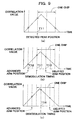
For example, as shown in Fig. 8(a), when values designated
with circles shown in Fig. 8(a) are sampled from a waveform of
a correlation value through two-times oversampling, a timing
T1 appearing at a "DETECTION PEAK POSITION" is taken as a timing
of a peakposition detected by the matched filter 20. Consequently,
when the received signal is demodulated while the timing T1 is
taken as a demodulation timing, a timing T2 is taken as an advanced
arm position, and timing T3 is taken as a delayed arm position.
In the example shown in Fig. 8, the phase of an operation
clock lags in phase behind the received signal. Hence, the
difference value becomes positive. When the difference value
exceeds the threshold value, the timing at which the HOLD signal
is to be brought into LOW is caused to advance by one clock.
As a result, as shown in Fig. 8(c), the demodulation timing
coincides timing T4. Thus, a timing closer to the peak position
can be taken as a demodulation timing. The embodiment shown in
Fig. 8 corresponds to Fig. 6(d).
As shown in Fig. 9(a), when a value designated by a circle
shown in Fig. 9(a) are sampled from a waveform of a correlation
value through two-times oversampling, a timing T11 appearing
at a "DETECTION PEAK POSITION" is taken as a timing of a peak
position detected by the matched filter 20. Consequently, when
the received signal is demodulated while the timing T11 is taken
as a demodulation timing, the timing T12 is taken as an advanced
arm position, as shown in Fig. 9(b).
In the embodiment shown in Fig. 9, the phase of an operation
clock leads the received signal. Hence, the difference value
becomes negative. When the difference value exceeds the threshold
value, the timing at which the HOLD signal is brought into low
is caused to lag by one clock. As shown in Fig. 9(c), the
demodulation timing coincides with a timing T14. Thus, a timing
closer to the peak position can be taken as a demodulation timing.
The embodiment shown in Fig. 9 corresponds to Fig. 6(c).
As shown in Fig. 6, a timing at which a LOW timing is to
be actually corrected is a timing which elapses "n" symbols ("n"
is an integer of 2 or more) from time T which takes, as a reference,
the path timing detected by the matched filter 20. In other words,
as shown in Fig. 6, the timing at which the LOW timing is to
be corrected is time T; that is, a timing at which "n" symbols
("n" is an integer of two or more) elapse from the timing at
which the HOLD signal has first been brought into low. A
difference value producedby averaging difference values computed
for "n" symbols is compared with the threshold value, thereby
determining whether or not the phase of a LOW timing is to be
shifted. A determination is made as to whether or not the phase
of the HOLD signal is corrected at a timing lapses "n" symbols
from the time T.
A difference for one symbol is computed at a point in time
after one symbol lapses from time T (see Fig. 6). Hence,
correction of a LOW timing is possible at this point in time.
The threshold value to be used for the timing adjustment
section 60 is set to such a value that a timing closer to the
peak position is achieved by shifting the timing at which the
HOLD signal is to be brought into low. Linear portions of
substantially-mountain-shaped graphs shown Figs. 8 and 9 are
enlarged views of a peak correlation value of the received signal.
Amethod of correcting the phase of a timing signal employed
in a CDMA communication scheme is performed in the foregoing
manner.
The timing adjustment section 60 outputs a HOLD signal
while a LOW timing thereof is corrected. On the basis of the
corrected LOW timing, a spreading code is output from the spreading
code generator 70 to the multiplier 42a, the multiplier 82, and
the multiplier 42b.
Then, the DLL 40 performs multiplication of the received
signal by the input spreading code and the like operation in
the same manner as mentioned above.
In the despread section 80, the multiplier 82 multiplies
the received signal by a spreading code output from the second
generator 74. A despread signal is output from the detector 84
by means of processing performed by the detector 84.
When the LOW timing of the HOLD signal is corrected, despread
processing is performed at a demodulation timing [i.e., a timing
T4 in the cases shown in Figs. 6(d) and 8 or a timing T14 in
the case shown in Figs. 6(c) and 9]. When the LOW timing of the
HOLD signal has been shifted through correction, a spreading
code is output to the despread section 80 at that LOW timing.
The multiplier 82 performs multiplication operation at that
timing. In other words, the corrected LOW timing acts as a
corrected demodulation timing.
The despread signal output from the despread section 80
is sent to the RAKE combiner section 90, where each of the fingers
30 performs an operation for generating a despread signal; that
is, a despread received signal. A received signal generated
through RAKE combiner is output to the outside by way of the
control section 100.
Naturally, when the phase of the HOLD signal is corrected,
the HOLD signal is brought into low at a predetermined cycle;
that is, every cycle of a chip rate frequency, until the phase
is corrected next time.
In relation to corrections to be performed subsequent to
the correction of the LOW timing of the HOLD signal, the phase
of a clock signal may be corrected so as to become shifted on,
e.g., a per-symbols basis in the same manner as mentioned above.
Specifically, a chance for correcting a phase is provided on
per-symbols basis. A determination may be made as to whether
or not the phase should be corrected, on a per-symbols basis.
Alternatively, there may be provided a chance for correcting
a phase on a per-symbol basis.
The descriptions have explained the receiver while an
operation for initial synchronization capturing is taken as an
example. However, a chance for correcting the phase of a HOLD
signal is not limited to a phase of initial synchronization
capturing and may be provided in a subsequent step.
As mentioned above, the receiver A of the embodiment detects
a rough path timing through use of a matched filter which is
activated at a low ratio of oversampling. At the time of
synchronization and holding of a synchronization with use of
a high ratio of oversampling, DLLs originally provided in fingers
for demodulation purposes are used, thereby reducing the size
of a circuit of the matched filter. The overall circuit scale
of the matched filter can be reduced. The receiver A of the
embodiment enables omission of processing to be performed by
the second circuit section of the CDMA receiver described in
Japanese Patent Application Laid-Open No. 82973/2000, thereby
contributing to a reduction in processing load. Eventually, the
receiver A of the embodiment can detect a peak position with
the accuracy of a sampling frequency of a received signal; that
is, the accuracy of four-times oversampling. Hence,
demodulation processing having a superior signal-to-noise ratio
can be performed.
As shown in Figs. 6(c) and 6(d), the descriptions have
explained that the LOW timing of the HOLD signal is corrected
at a timing which has lapsed "n" symbols ("n" is an integer of
two or more) from a time T while a path timing detected by the
matched filter 20 is taken as a reference. However, the invention
is not limited to such an example. The LOW timing may be corrected
at a timing located in the middle of certain symbols. More
specifically, an average of difference values of DLLs 40 for
n-1 symbols ("n" is an integer of three or more) is compared
with a predetermined threshold value, thereby rendering a
determination. When a LOW timing is to be corrected so as to
advance or lag, the timing is corrected at a position in an nth
symbol. If a LOW timing has been corrected, despread operation
is performed at a demodulation timing based on the corrected
LOW timing from the n+1th symbol.
The above descriptions have explained that, when a LOW
timing of the HOLD signal is corrected, the timing is caused
to advance or lag by one clock cycle. However, the invention
is not limited to this; the LOW timing may be caused to advance
or lag by a plurality of clock cycles.
In the descriptions, the first generator 72, the second
generator 74, and the third generator 76, all belonging to the
spreading code generator 70, output spreading codes while they
lag behind each other by a period corresponding to one-half a
chip. The description is based on that a period of time between
the timing at which the first generator 72 is to produce an output
and the timing at which the third generator 76 is to produce
an output is taken as one chip. Alternatively, the period of
time between the timing at which the first generator 72 is to
produce an output and the timing at which the third generator
76 is to produce an output is taken as a time "t" of two chips
or less. Further, a timing at which the second generator 74 is
to produce an output may lag behind the timing at which the first
generator 72 is to produce an output by half that time; that
is, by t/2. The time "t" corresponds to an expression "lag time"
in claims.
In the descriptions, the matched filter 20 has been
described as performing two-times oversampling operation, and
the fingers 30 have been described as performing four-times
oversampling operation. However, the invention is not limited
to those descriptions. So long as a matched filter is activated
at a frequency which is one-over-n ("n" is an integer of two
or more) times the sampling frequency of a received signal, other
cases are also conceivable; e.g., a case where the matched filter
20 performs two-times oversampling operation and the fingers
30 perform eight-times oversampling operation or a case where
the matched filter 20 performs two-times oversampling operation
and the fingers 30 perform 16-times oversampling operation.
The above descriptions have explained that a magnitude
of a difference value is compared with a predetermined threshold
value and that, when the magnitude of the difference value has
exceeded the threshold value, the phase of a HOLD signal is
corrected. Alternatively, a threshold value for a positive
difference value and another threshold value for a negative
difference value may also be provided. A difference value may
be compared with a corresponding threshold value. Specifically,
in a case where a threshold value for a positive difference value
is taken as S, a threshold value for a negative difference value
is taken as -S. In the case of a positive difference value, a
correction operation is performed when the difference value
exceeds S. In short, provided that a difference value is taken
as X, a correction operation is performed when S<X. In the case
of a negative difference value, a correction operation is
performed when the difference value is smaller than -S. In short,
provided that a difference value is taken as X, a correction
operation is performed when X < -S. Even such a case can be said
to yield the same result as that yielded by a method of performing
a correction operation when a difference value is determined
to exceed a threshold value as a result of the magnitude of the
difference value being compared with the threshold value.
Industrial Applicability
As mentioned above, at the time of CDMA receiving operation,
a receiver of the invention activates a matched filter to operate
at a frequency of one-over-n (where "n" is an integer) times
the sampling frequency of a received signal, thereby enabling
a reduction in a circuit scale of the matched filter. A
demodulation timing roughly grasped by the matched filter is
corrected on the basis of information output from DLLs. Since
the DLLs originally provided in the CDMA receiver are utilized,
the circuit scale of the receiver and loads stemming from
processing can be prevented from becoming greater.