EP1296387A2 - Highly moisture-sensitive electronic device element and method for fabrication utilizing vent holes or gaps - Google Patents
Highly moisture-sensitive electronic device element and method for fabrication utilizing vent holes or gaps Download PDFInfo
- Publication number
- EP1296387A2 EP1296387A2 EP02078700A EP02078700A EP1296387A2 EP 1296387 A2 EP1296387 A2 EP 1296387A2 EP 02078700 A EP02078700 A EP 02078700A EP 02078700 A EP02078700 A EP 02078700A EP 1296387 A2 EP1296387 A2 EP 1296387A2
- Authority
- EP
- European Patent Office
- Prior art keywords
- sensitive electronic
- highly moisture
- substrate
- moisture
- electronic device
- Prior art date
- Legal status (The legal status is an assumption and is not a legal conclusion. Google has not performed a legal analysis and makes no representation as to the accuracy of the status listed.)
- Withdrawn
Links
Images





Classifications
-
- G—PHYSICS
- G02—OPTICS
- G02F—OPTICAL DEVICES OR ARRANGEMENTS FOR THE CONTROL OF LIGHT BY MODIFICATION OF THE OPTICAL PROPERTIES OF THE MEDIA OF THE ELEMENTS INVOLVED THEREIN; NON-LINEAR OPTICS; FREQUENCY-CHANGING OF LIGHT; OPTICAL LOGIC ELEMENTS; OPTICAL ANALOGUE/DIGITAL CONVERTERS
- G02F1/00—Devices or arrangements for the control of the intensity, colour, phase, polarisation or direction of light arriving from an independent light source, e.g. switching, gating or modulating; Non-linear optics
- G02F1/01—Devices or arrangements for the control of the intensity, colour, phase, polarisation or direction of light arriving from an independent light source, e.g. switching, gating or modulating; Non-linear optics for the control of the intensity, phase, polarisation or colour
- G02F1/13—Devices or arrangements for the control of the intensity, colour, phase, polarisation or direction of light arriving from an independent light source, e.g. switching, gating or modulating; Non-linear optics for the control of the intensity, phase, polarisation or colour based on liquid crystals, e.g. single liquid crystal display cells
-
- H—ELECTRICITY
- H10—SEMICONDUCTOR DEVICES; ELECTRIC SOLID-STATE DEVICES NOT OTHERWISE PROVIDED FOR
- H10W—GENERIC PACKAGES, INTERCONNECTIONS, CONNECTORS OR OTHER CONSTRUCTIONAL DETAILS OF DEVICES COVERED BY CLASS H10
- H10W42/00—Arrangements for protection of devices
-
- H—ELECTRICITY
- H10—SEMICONDUCTOR DEVICES; ELECTRIC SOLID-STATE DEVICES NOT OTHERWISE PROVIDED FOR
- H10F—INORGANIC SEMICONDUCTOR DEVICES SENSITIVE TO INFRARED RADIATION, LIGHT, ELECTROMAGNETIC RADIATION OF SHORTER WAVELENGTH OR CORPUSCULAR RADIATION
- H10F39/00—Integrated devices, or assemblies of multiple devices, comprising at least one element covered by group H10F30/00, e.g. radiation detectors comprising photodiode arrays
- H10F39/80—Constructional details of image sensors
- H10F39/804—Containers or encapsulations
-
- H—ELECTRICITY
- H10—SEMICONDUCTOR DEVICES; ELECTRIC SOLID-STATE DEVICES NOT OTHERWISE PROVIDED FOR
- H10K—ORGANIC ELECTRIC SOLID-STATE DEVICES
- H10K59/00—Integrated devices, or assemblies of multiple devices, comprising at least one organic light-emitting element covered by group H10K50/00
- H10K59/80—Constructional details
- H10K59/87—Passivation; Containers; Encapsulations
- H10K59/871—Self-supporting sealing arrangements
-
- H—ELECTRICITY
- H10—SEMICONDUCTOR DEVICES; ELECTRIC SOLID-STATE DEVICES NOT OTHERWISE PROVIDED FOR
- H10K—ORGANIC ELECTRIC SOLID-STATE DEVICES
- H10K59/00—Integrated devices, or assemblies of multiple devices, comprising at least one organic light-emitting element covered by group H10K50/00
- H10K59/80—Constructional details
- H10K59/87—Passivation; Containers; Encapsulations
- H10K59/871—Self-supporting sealing arrangements
- H10K59/8722—Peripheral sealing arrangements, e.g. adhesives, sealants
-
- H—ELECTRICITY
- H10—SEMICONDUCTOR DEVICES; ELECTRIC SOLID-STATE DEVICES NOT OTHERWISE PROVIDED FOR
- H10K—ORGANIC ELECTRIC SOLID-STATE DEVICES
- H10K59/00—Integrated devices, or assemblies of multiple devices, comprising at least one organic light-emitting element covered by group H10K50/00
- H10K59/80—Constructional details
- H10K59/87—Passivation; Containers; Encapsulations
- H10K59/874—Passivation; Containers; Encapsulations including getter material or desiccant
-
- H—ELECTRICITY
- H10—SEMICONDUCTOR DEVICES; ELECTRIC SOLID-STATE DEVICES NOT OTHERWISE PROVIDED FOR
- H10W—GENERIC PACKAGES, INTERCONNECTIONS, CONNECTORS OR OTHER CONSTRUCTIONAL DETAILS OF DEVICES COVERED BY CLASS H10
- H10W76/00—Containers; Fillings or auxiliary members therefor; Seals
- H10W76/10—Containers or parts thereof
- H10W76/17—Containers or parts thereof characterised by their materials
- H10W76/18—Insulating materials, e.g. resins, glasses or ceramics
-
- H—ELECTRICITY
- H10—SEMICONDUCTOR DEVICES; ELECTRIC SOLID-STATE DEVICES NOT OTHERWISE PROVIDED FOR
- H10W—GENERIC PACKAGES, INTERCONNECTIONS, CONNECTORS OR OTHER CONSTRUCTIONAL DETAILS OF DEVICES COVERED BY CLASS H10
- H10W76/00—Containers; Fillings or auxiliary members therefor; Seals
- H10W76/40—Fillings or auxiliary members in containers, e.g. centering rings
- H10W76/42—Fillings
- H10W76/48—Fillings including materials for absorbing or reacting with moisture or other undesired substances
-
- H—ELECTRICITY
- H10—SEMICONDUCTOR DEVICES; ELECTRIC SOLID-STATE DEVICES NOT OTHERWISE PROVIDED FOR
- H10W—GENERIC PACKAGES, INTERCONNECTIONS, CONNECTORS OR OTHER CONSTRUCTIONAL DETAILS OF DEVICES COVERED BY CLASS H10
- H10W76/00—Containers; Fillings or auxiliary members therefor; Seals
- H10W76/60—Seals
-
- H—ELECTRICITY
- H10—SEMICONDUCTOR DEVICES; ELECTRIC SOLID-STATE DEVICES NOT OTHERWISE PROVIDED FOR
- H10F—INORGANIC SEMICONDUCTOR DEVICES SENSITIVE TO INFRARED RADIATION, LIGHT, ELECTROMAGNETIC RADIATION OF SHORTER WAVELENGTH OR CORPUSCULAR RADIATION
- H10F39/00—Integrated devices, or assemblies of multiple devices, comprising at least one element covered by group H10F30/00, e.g. radiation detectors comprising photodiode arrays
- H10F39/80—Constructional details of image sensors
-
- H—ELECTRICITY
- H10—SEMICONDUCTOR DEVICES; ELECTRIC SOLID-STATE DEVICES NOT OTHERWISE PROVIDED FOR
- H10K—ORGANIC ELECTRIC SOLID-STATE DEVICES
- H10K71/00—Manufacture or treatment specially adapted for the organic devices covered by this subclass
- H10K71/851—Division of substrate
-
- H—ELECTRICITY
- H10—SEMICONDUCTOR DEVICES; ELECTRIC SOLID-STATE DEVICES NOT OTHERWISE PROVIDED FOR
- H10W—GENERIC PACKAGES, INTERCONNECTIONS, CONNECTORS OR OTHER CONSTRUCTIONAL DETAILS OF DEVICES COVERED BY CLASS H10
- H10W70/00—Package substrates; Interposers; Redistribution layers [RDL]
- H10W70/60—Insulating or insulated package substrates; Interposers; Redistribution layers
- H10W70/67—Insulating or insulated package substrates; Interposers; Redistribution layers characterised by their insulating layers or insulating parts
- H10W70/68—Shapes or dispositions thereof
- H10W70/681—Shapes or dispositions thereof comprising holes not having chips therein, e.g. for outgassing, underfilling or bond wire passage
Definitions
- the present invention relates to control of moisture inside a packaged electronic device and relates particularly to highly moisture-sensitive electronic device elements having multiple highly moisture-sensitive electronic devices and methods for their fabrication to prevent premature device failure or premature degradation of device performance.
- electronic devices are typically produced by fabricating large substrates containing multiple electronic devices. These substrates are typically selected from the group consisting of glass, plastic, metal, ceramic, silicon and other semiconductor materials, or combinations of these materials.
- the substrates may be rigid or flexible and may be handled as individual units or continuous rolls.
- the primary reason for fabricating multiple electronic devices on large individual substrates or a continuous roll substrate is to reduce manufacturing cost by decreasing handling, increasing throughput, and increasing yield.
- silicon wafer processing has increased from 2 inch wafers to 12 inch wafers resulting in significant cost reductions.
- liquid crystal display (LCD) industry glass substrate processing has increased from 300 mm x 400 mm substrates to over 600 mm x 700 mm substrates with the same result.
- FIG. 1A shows an unencapsulated highly moisture-sensitive electronic device element 14 containing multiple highly moisture-sensitive electronic devices 12 on an individual substrate 10
- FIG. 1B is a schematic sectional view of the highly moisture-sensitive electronic device element 14 taken along section line 1B-1B of FIG. 1A.
- Typical electronic devices require humidity levels in a range of about 2500 to below 5000 parts per million (ppm) to prevent premature degradation of device performance within a specified operating and/or storage life of the device. Control of the environment to this range of humidity levels within a packaged device is typically achieved by encapsulating the device or by sealing the device and a desiccant within a cover. Desiccants such as, for example, molecular sieve materials, silica gel materials, and materials commonly referred to as Drierite materials, are used to maintain the humidity level within the above range. Short term exposure to humidity levels greater than 2500 ppm during the fabrication and encapsulation of these types of electronic devices typically does not cause measurable degradation of device performance. For this reason, encapsulation of these types of electronic devices is done after the electronic devices are separated from the initial substrate.
- FIG. 2A shows a typical multiple LCD element 28 before separation into single LCD devices
- FIG. 2B is a schematic sectional view of the multiple LCD element 28 taken along section line 2B-2B of FIG. 2A.
- LCD manufacturing the LCD back-plane 22 and the LCD front-plane 24 contain multiple LCD devices.
- the LCD back-plane 22 and the LCD front-plane 24 are bonded together with a sealing material 20 that surrounds each LCD device except for a gap in the sealing material 20.
- the LCD devices are separated and filled with liquid crystal material.
- the gap in the sealing material 20 is sealed with a gap sealing material to retain the liquid crystal material and to protect the LCD back-plane electronics 26 and the liquid crystal material from moisture. Because LCD devices are not highly moisture-sensitive, the separation process of the multiple LCD element is typically performed in an ambient air environment with no measurable degradation of the LCD devices.
- OLED organic light-emitting devices
- CCD charge-coupled device
- MEMS micro-electro-mechanical sensors
- molecular sieve materials have a relatively low moisture capacity at humidity levels at or below 1000 ppm, and the minimum achievable humidity level of molecular sieve materials is a function of temperature within an enclosure: moisture absorbed, for example, at room temperature, can be released into the enclosure or package during temperature cycling to higher temperature, such, as, for example, to a temperature of 100°C.
- Desiccants used within such packaged devices include powders of metal oxides, alkaline earth metal oxides, sulfates, metal halides, or perchlorates, that is, materials having desirably relatively low values of equilibrium minimum humidity and high moisture capacity.
- such materials often chemically absorb moisture relatively slowly compared to the above-mentioned molecular sieve, silica gel, or Drierite materials.
- highly moisture-sensitive devices such as organic light-emitting devices (OLED) or panels, polymer light-emitting devices, charge-coupled device (CCD) sensors, and micro-electro-mechanical sensors (MEMS)
- OLED organic light-emitting devices
- CCD charge-coupled device
- MEMS micro-electro-mechanical sensors
- FIG. 3A shows a typical multiple OLED element 34 containing multiple OLED devices 32 on an individual substrate 10, encapsulated with individual encapsulation enclosures 30 and sealing material 20, and FIG. 3B is a schematic sectional view of the multiple OLED element 34 taken along section line 3B-3B of FIG. 3A.
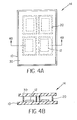
- FIG. 4A shows a highly moisture-sensitive electronic device element 14 comprising a substrate 10 containing multiple highly moisture-sensitive electronic devices 12, a single encapsulation enclosure 30 encapsulating all of the highly moisture-sensitive electronic devices 12, and sealing material 20.
- the problem with this technique is shown schematically in FIG. 4A where the sealing material 20 has been damaged by the high gas pressure inside each seal region produced when the substrate 10 and the encapsulation enclosure 30 are moved to their predetermined spacing after both the substrate and the encapsulation enclosure have contacted the sealing material.
- FIG. 4B is a schematic sectional view of the highly moisture-sensitive electronic device element 14 taken along section lines 4B-4B of FIG. 4A. It would, therefore, be desirable to have highly moisture-sensitive electronic device elements and a method for fabricating highly moisture-sensitive electronic device elements that does not damage the seals that are required to protect the highly moisture-sensitive electronic devices from moisture during fabrication and encapsulation.
- Kawami and others disclose an organic EL element enclosed in an airtight container which contains a drying substance comprised of a solid compound for chemically absorbing moisture. The drying substance is spaced from the organic EL element, and the drying substance is consolidated in a predetermined shape by vacuum vapor deposition, sputtering, or spin-coating. Kawami and others teach the use of the following desiccants: alkali metal oxides, alkali earth metal oxides, sulfates, metal halides, and perchlorates.
- Kawami and others do not teach a multiple EL device element with multiple airtight containers nor a method for fabricating a multiple EL device element with multiple airtight containers.
- the handling and sealing problems and solutions of a multiple EL device element, such as methods to prevent damage to the seal due to high gas pressure inside the seal region during encapsulation, are not discussed nor taught by Kawami and others.
- Shores, US-A-5,304,419 discloses a moisture and particle getter for enclosures which enclose an electronic device. A portion of an inner surface of the enclosure is coated with a pressure sensitive adhesive containing a solid desiccant.
- Shores, US-A-5,401,536, describes a method of providing a moisture-free enclosure for an electronic device, the enclosure containing a coating or adhesive with desiccant properties.
- the coating or adhesive comprises a protonated alumina silicate powder dispersed in a polymer.
- compositions for hermetic electronic devices.
- the composition is applied as a coating or adhesive to the interior surface of a device packaging, and the composition comprises a water vapor permeable binder which has dispersed therein a desiccant, which is preferably a molecular sieve material.
- Booe US-A-4,081,397, describes a composition used for stabilizing the electrical and electronic properties of electrical and electronic devices.
- the composition comprises alkaline earth oxides in an elastomeric matrix.
- Booe does not teach a multiple device element or a method used for stabilizing the electrical and electronic properties of a multiple electrical and electronic device element.
- US-A-4,357,557 describe a thin-film electroluminescent display panel sealed by a pair of glass substrates for protection from the environment.
- the method includes a protective liquid introduced between the glass substrates, a spacer positioned for determining the spacing between the pair of substrates, injection holes formed within one of the substrates to withdraw under vacuum the air and gases from the cavity defined by the substrates and to introduce the protective liquid into the cavity, an adhesive adapted to provide bonding between the substrates and the spacer, a moisture absorptive member introduced into the protective liquid, and an adhesive to seal the injection hole.
- Inohara and others do not teach a multiple EL device element with multiple airtight containers nor a method for fabricating a multiple EL device element with multiple airtight containers.
- the handling and sealing problems and solutions of a multiple EL device element such as methods to prevent damage to the seal due to high gas pressure inside the seal region during encapsulation, are not discussed nor taught by Inohara and others.
- the use of injection holes in one of the substrates will prevent damage to the seal by permitting excess ambient gas to exit through the injection holes during encapsulation, Inohara and others do not teach this purpose for providing the injection holes. Instead the purpose of the injection holes is to allow introduction of the protective liquid into the cavity defined by the substrates.
- Taniguchi and others US-A-5,239,228, describe a method for protecting a thin-film electroluminescent device similar to Inohara and others with the additional feature of a groove in the sealing plate to capture excess adhesive. This groove may also contain a moisture absorption agent. Taniguchi and others also do not teach a multiple EL device element with multiple airtight containers nor a method for fabricating a multiple EL device element with multiple airtight containers. The handling and sealing problems and solutions of a multiple EL device element, such as methods to prevent damage to the seal due to high gas pressure inside the seal region during encapsulation, are also not discussed nor taught by Taniguchi and others.
- Harvey, III and others US-A-5,771,562, describe a method of hermetically sealing organic light-emitting devices comprising the steps of providing an organic light-emitting device on a substrate, overcoating the organic light-emitting device with a film of inorganic dielectric material, and sealingly engaging an inorganic layer over the dielectric material.
- Harvey, III and others do not teach a multiple OLED device element with multiple airtight containers nor a method for fabricating a multiple OLED device element with multiple airtight containers.
- the inorganic dielectric layer may provide temporary protection from moisture during the encapsulation process, Harvey, III and others do not teach how this layer can be used to fabricate a multiple OLED device element with multiple airtight containers.
- US-A-6,226,890 describe a method of desiccating an environment surrounding a highly moisture-sensitive electronic device sealed within an enclosure, including selecting a desiccant comprised of solid particles having a particle size range 0.1 to 200 micrometers.
- the desiccant is selected to provide an equilibrium minimum humidity level lower than a humidity level to which the device is sensitive within the sealed enclosure.
- a binder is chosen that maintains or enhances the moisture absorption rate of the desiccant for blending the selected desiccant therein.
- the binder may be in liquid phase or dissolved in a liquid.
- a castable blend is formed including at least the desiccant particles and the binder, the blend having a preferred weight fraction of the desiccant particles in the blend in a range of 10% to 90%.
- the blend is cast in a measured amount onto a portion of an interior surface of an enclosure to form a desiccant layer thereover, the enclosure having a sealing flange.
- the blend is solidified to form a solid desiccant layer, and the electronic device is sealed with the enclosure along the sealing flange.
- Boroson and others do not teach a method of desiccating an environment surrounding a multiple highly moisture-sensitive electronic device element sealed within multiple enclosures.
- a highly moisture-sensitive electronic device element having highly moisture-sensitive electronic devices comprising:
- this object is achieved by a method of making highly moisture-sensitive electronic device elements having a plurality of highly moisture-sensitive electronic devices such as OLED devices on a single substrate wherein the devices are protected from moisture prior to separating the individual devices from the substrate, comprising the steps of:
- the elements and methods for fabrication of the elements in accordance with the present invention of highly moisture-sensitive electronic device elements having highly moisture-sensitive electronic devices and methods for their fabrication to prevent premature device failure or premature degradation of device performance provides the following advantages over prior art methods: reduced handling of devices and encapsulation enclosures by sealing all of the highly moisture-sensitive devices on a single substrate as a single element with a single encapsulation enclosure encapsulating all of the highly moisture-sensitive electronic devices on the substrate prior to separating into smaller single or multiple device elements; improved protection from moisture prior to exposure to ambient environments; improved compatibility with automated processes required for high volume manufacturing; improved compatibility with processing inside a low moisture environment; and reduction in encapsulation defects due to pressure differentials inside and outside the highly moisture-sensitive electronic devices.
- highly moisture-sensitive electronic device element is employed to designate an element that contains one or more highly moisture-sensitive electronic devices during or after fabrication, or both, during and after fabrication of the highly moisture-sensitive electronic devices is complete.
- highly moisture-sensitive electronic device is employed to designate any electronic device that is susceptible to a measurable degradation of device performance at ambient moisture levels greater than 1000 ppm.
- substrate is employed to designate organic, inorganic, or combination organic and inorganic solids on which one or more highly moisture-sensitive electronic devices are fabricated.
- encapsulation enclosure is employed to designate organic, inorganic, or combination organic and inorganic solids used to protect one or more highly moisture-sensitive electronic devices from moisture by preventing or limiting moisture permeation through the encapsulation enclosures.
- sealing material is employed to designate organic, inorganic, or combination organic and inorganic materials used to bond encapsulation enclosures to substrates and to protect one or more highly moisture-sensitive electronic devices from moisture by preventing or limiting moisture permeation through the sealing materials.
- gap is employed to designate a discontinuity in the sealing material surrounding one or more electronic devices.
- water absorbing material is employed to designate inorganic materials used to physically or chemically absorb or react with moisture that would otherwise damage the highly moisture-sensitive electronic devices.
- temporary moisture protection layer is employed to designate organic, inorganic, or combination organic and inorganic materials used to prevent or limit moisture induced damage to the highly moisture-sensitive electronic devices during short term exposure to ambient moisture levels greater than 1000 ppm, where short term is typically less than 10 days.
- FIG. 5A there is shown one embodiment of the highly moisture-sensitive electronic device element 14 in accordance with the present invention.
- a highly moisture-sensitive electronic device element 14 is shown comprising a substrate 10 containing multiple highly moisture-sensitive electronic devices 12, a single encapsulation enclosure 30 encapsulating all of the highly moisture-sensitive electronic devices 12 on the substrate 10, and sealing material 20 surrounding each highly moisture-sensitive electronic device 12 with no gaps in the sealing material 20.
- FIG. 5B is a schematic sectional view of the highly moisture-sensitive electronic device element 14 taken along section lines 5B-5B of FIG. 5A. In FIG. 5A and FIG.
- the highly moisture-sensitive electronic device element 14 is shown comprising four highly moisture-sensitive electronic devices 12, but the highly moisture-sensitive electronic device element of this invention may comprise any number of highly moisture-sensitive electronic devices greater than one.
- the substrate 10 and the encapsulation enclosure 30 shown in FIG. 5A and FIG. 5B may be an organic solid, an inorganic solid, or a combination of organic and inorganic solids.
- the substrate and the encapsulation enclosure may be rigid or flexible and may be processed as separate individual pieces, such as sheets or wafers, or as a continuous roll.
- Typical substrate and encapsulation enclosure materials include glass, plastic, metal, ceramic, semiconductor, metal oxide, metal nitride, metal sulfide, semiconductor oxide, semiconductor nitride, semiconductor sulfide, carbon, or combinations thereof.
- the substrate and the encapsulation enclosure may be a homogeneous mixture of materials, a composite of materials, or multiple layers of materials.
- the substrate, the encapsulation enclosure, or both, contain vent holes 100 and vent hole seal material 102.
- the vent hole seal material can be the same material as the sealing material used to bond the substrate and the encapsulation enclosure or may be a different enclosing material.
- the vent hole enclosing material may be organic, inorganic, or a combination thereof. Examples of enclosing materials are adhesives, solders, tapes, multilayer laminates bonded with adhesive, and inorganic covers bonded with adhesive.
- the sealing material 20 shown in FIG. 5A and FIG. 5B surrounds each individual highly moisture-sensitive electronic device, but the sealing material could also surround groups of two or more highly moisture-sensitive electronic devices if the final product required more than one highly moisture-sensitive electronic device within a single element.
- the sealing material surrounding each highly moisture-sensitive electronic device or groups of highly moisture-sensitive electronic devices contains no gaps such that the highly moisture-sensitive electronic device element is protected from moisture prior to separating into smaller single or multiple device elements.
- the sealing material may be organic, inorganic, or a combination of organic and inorganic.
- the sealing material may be bonded to the substrate and the encapsulation enclosure by melting and cooling or by reaction curing. Typical materials bonded by melting and cooling include glass; hot melt adhesives such as polyolefins, polyesters, polyamides, or combinations thereof; or inorganic solders such as indium, tin, lead, silver, gold, or combinations thereof.
- Typical reaction curing methods include reactions resulting from heat, radiation such as UV radiation, mixing of two or more components, exposure to ambient moisture, removal of ambient oxygen, or combinations thereof.
- Typical materials bonded by reaction curing include acrylates, epoxies, polyurethanes, silicones, or combinations thereof.
- Other inorganic material typically used in sealing materials include glass, ceramic, metal, semiconductor, metal oxide, semiconductor oxide, or combinations thereof.
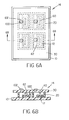
- FIG. 6A there is shown another embodiment of the highly moisture-sensitive electronic device element 14 in accordance with the present invention.
- a highly moisture-sensitive electronic device element 14 is shown comprising a substrate 10 containing multiple highly moisture-sensitive electronic devices 12, a single encapsulation enclosure 30 encapsulating all of the highly moisture-sensitive electronic devices 12 on the substrate 10, sealing material 20 defining a space surrounding each highly moisture-sensitive electronic device 12 with no gaps in the sealing material 20, water absorbing material 60 positioned between the substrate 10 and the encapsulation enclosure 30 and within the space defined by the sealing material 20, and temporary moisture protection layers 62 coated over each of the highly moisture-sensitive electronic devices 12.
- FIG. 6B is a schematic sectional view of the highly moisture-sensitive electronic device element 14 taken along section lines 6B-6B of FIG.
- FIG. 6A Details of the highly moisture-sensitive electronic devices 12, substrate 10, encapsulation enclosure 30, and sealing material 20 are identical with the embodiment shown in FIG. 5A and FIG. 5B. Also as in the embodiment shown in FIG. 5A and FIG. 5B, the substrate, the encapsulation enclosure, or both, contain vent holes 100 and vent hole seal material 102. Details of the vent hole seal material are identical with the embodiment shown in FIG. 5A and FIG. 5B.
- the water absorbing material is used to physically or chemically absorb or react with moisture that would otherwise damage the highly moisture-sensitive electronic devices.
- Typical water absorbing materials include alkaline metal oxides, alkaline earth metal oxides, sulfates, metal halides, perchlorates, molecular sieves, and metals with work functions less than 4.5 eV and capable of being oxidized in the presence of moisture, or combinations thereof.
- Water absorbing material may be packaged within moisture permeable containers or binders.
- the water absorbing material may be a single material, a homogeneous mixture of materials, a composite of materials, or multiple layers of materials.
- Temporary moisture protection layers are used to prevent or limit moisture induced damage to the highly moisture-sensitive electronic devices during short term exposure to ambient moisture levels greater than 1000 ppm.
- the temporary moisture protection layer is organic material, inorganic material, or a combination thereof.
- Typical organic materials include epoxies, polyurethanes, polyureas, acrylates, silicones, polyamides, polyimides, phenolics, polyvinyls, phenoxies, polysulfones, polyolefins, polyesters, or combinations thereof.
- Typical inorganic materials include glass, ceramic, metal, semiconductor, metal oxide, metal nitride, metal sulfide, semiconductor oxide, semiconductor nitride, semiconductor sulfide, carbon, or combinations thereof.
- the temporary moisture protection layer may be a single material, a homogeneous mixture of materials, a composite of materials, or multiple layers of materials.
- FIGS. 7A to 7D there is shown an embodiment of the method of making highly moisture-sensitive electronic device elements having a plurality of highly moisture-sensitive electronic devices such as OLED devices on a single substrate wherein the devices are protected from moisture prior to separating the individual devices from the substrate in accordance with the present invention.
- FIG. 7A shows a highly moisture-sensitive electronic device element 14 comprising a substrate 10 containing multiple highly moisture-sensitive electronic devices 12, sealing material 20 surrounding each highly moisture-sensitive electronic device 12 with no gaps in the sealing material 20, and a vent hole 100 through the substrate for each highly moisture-sensitive electronic device 12 in close aligned proximity to, but spaced apart from, an encapsulation enclosure 30 encapsulating all of the highly moisture-sensitive electronic devices 12 on the substrate 10.
- FIG. 7A shows a highly moisture-sensitive electronic device element 14 comprising a substrate 10 containing multiple highly moisture-sensitive electronic devices 12, sealing material 20 surrounding each highly moisture-sensitive electronic device 12 with no gaps in the sealing material 20, and a vent hole 100 through the substrate for each highly moisture-sensitive electronic device 12
- FIG. 7B is a schematic sectional view of the highly moisture-sensitive electronic device element 14 taken along section lines 7B,C,D-7B,C,D of FIG. 7A.
- the ambient pressure may be above, below, or equal to atmospheric pressure.
- Details of the highly moisture-sensitive electronic devices 12, substrate 10, encapsulation enclosure 30, and sealing material 20 are identical with the embodiment shown in FIG. 5A and 5B.
- the water absorbing material 60, temporary moisture protection layer 62 ,or both, described in detail in the embodiment shown in FIG. 6A and 6B may be coated on the highly moisture-sensitive electronic devices 12 or on the encapsulation enclosure.
- the vent holes may be through the encapsulation enclosure or through both the substrate and the encapsulation enclosure.
- FIG. 7C is a schematic sectional view of the highly moisture-sensitive electronic device element 14 taken along section lines 7B,C,D-7B,C,D of FIG. 7A after relative motion 90 of the substrate 10 and the encapsulation enclosure 30 to the point where the substrate 10 and the encapsulation enclosure 30 are spaced apart within a predetermined range, excess ambient gas has exited through the vent holes 100, and the sealing material 20 has been bonded to both the substrate 10 and the encapsulation enclosure 30. Because excess gas may exit through the vent holes, the ambient surrounding the substrate 10, the encapsulation enclosure 30, and the sealing material 20 is equal to the pressure within spaces defined between the substrate 10, the encapsulation enclosure 30, and the sealing material 20, thereby preventing deformation of the sealing material 20.
- Bonding the sealing material 20 to both the substrate 10 and the encapsulation enclosure 30 may be accomplished by melting and cooling, reaction curing, or a combination thereof.
- the reaction curing may include reactions resulting from heat, radiation, mixing of two or more components, exposure to ambient moisture, removal of ambient oxygen, or combinations thereof.
- FIG. 7D is a schematic sectional view of the highly moisture-sensitive electronic device element taken along section lines 7B,C,D-7B,C,D of FIG. 7A after sealing the vent holes with vent hole seal material.
- the vent holes may be sealed before or during bonding of the sealing material to the substrate and the encapsulation body. Details of the vent hole seal material are identical with the embodiment shown in FIG. 5A and FIG. 5B.
- FIGS. 8A to 8E there is shown another embodiment of the method of making highly moisture-sensitive electronic device elements having a plurality of highly moisture-sensitive electronic devices such as OLED devices on a single substrate wherein the devices are protected from moisture prior to separating the individual devices from the substrate in accordance with the present invention.
- FIG. 8A shows a highly moisture-sensitive electronic device element 14 comprising a substrate 10 containing multiple highly moisture-sensitive electronic devices 12 and sealing material 20 surrounding each highly moisture-sensitive electronic device 12 with gaps in the sealing material 20 in close aligned proximity to, but spaced apart from, an encapsulation enclosure 30 encapsulating all of the highly moisture-sensitive electronic devices 12 on the substrate 10.
- FIG. 8A shows a highly moisture-sensitive electronic device element 14 comprising a substrate 10 containing multiple highly moisture-sensitive electronic devices 12 and sealing material 20 surrounding each highly moisture-sensitive electronic device 12 with gaps in the sealing material 20 in close aligned proximity to, but spaced apart from, an encapsulation enclosure 30 encapsulating all of the highly moisture-sensitive electronic devices 12 on
- FIG. 8B is a schematic sectional view of the highly moisture-sensitive electronic device element 14 taken along section lines 8B,C-8B,C of FIG. 8A.
- the ambient pressure may be above, below, or equal to atmospheric pressure.
- Details of the highly moisture-sensitive electronic devices 12, substrate 10, encapsulation enclosure 30, and sealing material 20 are identical with the embodiment shown in FIG. 5A and 5B.
- the water absorbing material 60, temporary moisture protection layer 62, or both, described in detail in the embodiment shown in FIG. 6A and 6B may be coated on the highly moisture-sensitive electronic devices 12 or on the encapsulation enclosure.
- FIG. 8C is a schematic sectional view of the highly moisture-sensitive electronic device element 14 taken along section lines 8B,C-8B,C of FIG. 8A after relative motion 90 of the substrate 10 and the encapsulation enclosure 30 to the point where the sealing material 20 contacts both the substrate 10 and the encapsulation enclosure 30.
- FIG. 8D shows a highly moisture-sensitive electronic device element 14 after relative motion between the substrate 10 and the encapsulation enclosure 30 to a predetermined spacing range, during which excess ambient gas escapes through the gaps until the gaps are filled by spreading the sealing material, and after the sealing material 20 has been bonded to both the substrate 10 and the encapsulation enclosure 30.
- FIG. 8E is a schematic sectional view of the highly moisture-sensitive electronic device element taken along section lines 8E-8E of FIG.
- the gap size is selected such that the gap will fill in by spreading of the sealing material during the step where the substrate and the encapsulation enclosure are moved to their final predetermined spacing range. Because excess gas may exit through the gap, the pressure difference within spaces defined between the substrate 10, the encapsulation enclosure 30, and the sealing material 20 relative to the ambient pressure is reduced to thereby prevent deformation of the sealing material 20. Bonding the sealing material 20 to both the substrate 10 and the encapsulation enclosure 30 may be accomplished by the same methods described in the embodiment of FIG. 7A to 7D. After completing the method described in FIG. 8A to 8E, the highly moisture-sensitive electronic devices are typically separated into individual devices or groups of devices having a portion of the initial substrate.
- test structures were fabricated by the following process sequence:
- the quality of the encapsulation for all locations within the test structure was judged based on the quality of the sealing material after bonding. If damage was evident to the seal material due to pressure differences inside and outside the sealing material, the encapsulation quality was rated as poor. If no damage was evident, the encapsulation quality was rated as good. If slight damage was evident, the encapsulation quality was rated as fair. The test structures with vent holes all had encapsulation quality rated as good. The control test structures without vent holes all had encapsulation quality rated as poor.
- the highly moisture-sensitive electronic device element wherein the substrate includes rigid or flexible: glass, plastic, metal, ceramic, semiconductor, metal oxide, metal nitride, metal sulfide, semiconductor oxide, semiconductor nitride, semiconductor sulfide, carbon, or combinations thereof.
- the highly moisture-sensitive electronic device element wherein the encapsulation enclosure includes rigid or flexible: glass, plastic, metal, ceramic, semiconductor, metal oxide, metal nitride, metal sulfide, semiconductor oxide, semiconductor nitride, semiconductor sulfide, carbon, or combinations thereof.
- the highly moisture-sensitive electronic device element wherein the sealing material is organic material, inorganic material, or combinations thereof that is melted and cooled or reaction cured.
- reaction curing includes reactions resulting from heat, radiation, mixing of two or more components, exposure to ambient moisture, removal of ambient oxygen, or combinations thereof.
- the highly moisture-sensitive electronic device element wherein the organic material is selected from the group consisting of epoxies, polyurethanes, acrylates, silicones, polyamides, polyolefins, and polyesters, or combinations thereof.
- the highly moisture-sensitive electronic device element wherein the inorganic material is selected from the group consisting of glass, ceramic, metal, semiconductor, metal oxide, semiconductor oxide, and metal solder, or combinations thereof.
- the highly moisture-sensitive electronic device element wherein the water absorbing material is selected from the group consisting of alkaline metal oxides, alkaline earth metal oxides, sulfates, metal halides, perchlorates, molecular sieves, and metals with work functions less than 4.5 eV and capable of being oxidized in the presence of moisture, or combinations thereof.
- the highly moisture-sensitive electronic device element wherein the sealing material or other enclosing material is used to seal the vent holes.
- the highly moisture-sensitive electronic device element wherein the enclosing material is organic, inorganic, or a combination thereof.
- a highly moisture-sensitive electronic device element having highly moisture-sensitive electronic devices comprising:
- the highly moisture-sensitive electronic device element wherein the substrate includes rigid or flexible: glass, plastic, metal, ceramic, semiconductor, metal oxide, metal nitride, metal sulfide, semiconductor oxide, semiconductor nitride, semiconductor sulfide, carbon, or combinations thereof.
- the highly moisture-sensitive electronic device element wherein the encapsulation enclosure includes rigid or flexible: glass, plastic, metal, ceramic, semiconductor, metal oxide, metal nitride, metal sulfide, semiconductor oxide, semiconductor nitride, semiconductor sulfide, carbon, or combinations thereof.
- the highly moisture-sensitive electronic device element wherein the sealing material is organic material, inorganic material, or combinations thereof that is melted and cooled or reaction cured.
- reaction curing includes reactions resulting from heat, radiation, mixing of two or more components, exposure to ambient moisture, removal of ambient oxygen, or combinations thereof.
- the highly moisture-sensitive electronic device element wherein the organic material is selected from the group consisting of epoxies, polyurethanes, acrylates, silicones, polyamides, polyolefins, and polyesters, or combinations thereof.
- the highly moisture-sensitive electronic device element wherein the inorganic material is selected from the group consisting of glass, ceramic, metal, semiconductor, metal oxide, semiconductor oxide, and metal solder, or combinations thereof.
- the highly moisture-sensitive electronic device element wherein the temporary moisture protection layer is organic material, inorganic material, or a combination thereof.
- the highly moisture-sensitive electronic device element wherein the organic material is selected from the group consisting of epoxies, polyurethanes, polyureas, acrylates, silicones, polyamides, polyimides, phenolics, polyvinyls, phenoxies, polysulfones, polyolefins, and polyesters, or combinations thereof.
- the highly moisture-sensitive electronic device element wherein the inorganic material is selected from the group consisting of glass, ceramic, metal, semiconductor, metal oxide, metal nitride, metal sulfide, semiconductor oxide, semiconductor nitride, semiconductor sulfide, and carbon, or combinations thereof.
- the highly moisture-sensitive electronic device element wherein the sealing material or other enclosing material is used to seal the vent holes.
- the highly moisture-sensitive electronic device element wherein the enclosing material is organic, inorganic, or a combination thereof.
- a method of making highly moisture-sensitive electronic device elements having a plurality of highly moisture-sensitive electronic devices such as OLED devices on a single substrate wherein the devices are protected from moisture prior to separating the individual devices from the substrate comprising the steps of:
- the method wherein the enclosing material is organic, inorganic, or a combination thereof.
- the method wherein the bonding step is accomplished by melting and cooling, reaction curing, or a combination thereof.
- reaction includes reactions resulting from heat, radiation, mixing of two or more components, exposure to ambient moisture, removal of ambient oxygen, or combinations thereof.
- the substrate includes rigid or flexible: glass, plastic, metal, ceramic, semiconductor, metal oxide, metal nitride, metal sulfide, semiconductor oxide, semiconductor nitride, semiconductor sulfide, carbon, or combinations thereof.
- the encapsulation enclosure includes rigid or flexible: glass, plastic, metal, ceramic, semiconductor, metal oxide, metal nitride, metal sulfide, semiconductor oxide, semiconductor nitride, semiconductor sulfide, carbon, or combinations thereof.
- sealing material is organic material, inorganic material, or combinations thereof.
- organic material is selected from the group consisting of epoxies, polyurethanes, acrylates, silicones, polyamides, polyolefins, and polyesters, or combinations thereof.
- the method wherein the inorganic material is selected from the group consisting of glass, ceramic, metal, semiconductor, metal oxide, semiconductor oxide, and metal solder, or combinations thereof.
- the method further including the step of separating the highly moisture-sensitive electronic devices into individual devices or groups of devices having a portion of the initial substrate.
- the method further including the step of coating a substrate containing two or more highly moisture-sensitive electronic devices with a temporary moisture protection layer; or coating a water absorbing material onto either the substrate or an encapsulation enclosure in positions on the substrate or on the encapsulation enclosure such that after bonding, the water absorbing material will be positioned within each highly moisture-sensitive electronic device or within each group of highly moisture-sensitive electronic devices; or coating both said temporary moisture protection layer and said water absorbing material.
- the water absorbing material is selected from the group consisting of alkaline metal oxides, alkaline earth metal oxides, sulfates, metal halides, perchlorates, molecularsieves, and metals with work functions less than 4.5 eV and capable of being oxidized in the presence of moisture, or combinations thereof.
- the temporary moisture protection layer is organic material, inorganic material, or a combination thereof.
- organic material is selected from the group consisting of epoxies, polyurethanes, polyureas, acrylates, silicones, polyamides, polyimides, phenolics, polyvinyls, phenoxies, polysulfones, polyolefins, and polyesters, or combinations thereof.
- the inorganic material is selected from the group consisting of glass, ceramic, metal, semiconductor, metal oxide, metal nitride, metal sulfide, semiconductor oxide, semiconductor nitride, semiconductor sulfide, and carbon, or combinations thereof.
- a method of making highly moisture-sensitive electronic device elements having a plurality of highly moisture-sensitive electronic devices such as OLED devices on a single substrate wherein the devices are protected from moisture prior to separating the individual devices from the substrate comprising the steps of:
- the method wherein the bonding step is accomplished by melting and cooling, reaction curing, or a combination thereof.
- reaction includes reactions resulting from heat, radiation, mixing of two or more components, exposure to ambient moisture, removal of ambient oxygen, or combinations thereof.
- the substrate includes rigid or flexible: glass, plastic, metal, ceramic, semiconductor, metal oxide, metal nitride, metal sulfide, semiconductor oxide, semiconductor nitride, semiconductor sulfide, carbon, or combinations thereof.
- the encapsulation enclosure includes rigid or flexible: glass, plastic, metal, ceramic, semiconductor, metal oxide, metal nitride, metal sulfide, semiconductor oxide, semiconductor nitride, semiconductor sulfide, carbon, or combinations thereof.
- sealing material is organic material, inorganic material, or combinations thereof.
- organic material is selected from the group consisting of epoxies, polyurethanes, acrylates, silicones, polyamides, polyolefins, and polyesters, or combinations thereof.
- the method wherein the inorganic material is selected from the group consisting of glass, ceramic, metal, semiconductor, metal oxide, semiconductor oxide, and metal solder, or combinations thereof.
- the method further including the step of separating the highly moisture-sensitive electronic devices into individual devices or groups of devices having a portion of the initial substrate.
- the method further including the step of coating a substrate containing two or more highly moisture-sensitive electronic devices with a temporary moisture protection layer; or coating a water absorbing material onto either the substrate or an encapsulation enclosure in positions on the substrate or on the encapsulation enclosure such that after bonding, the water absorbing material will be positioned within each highly moisture-sensitive electronic device or within each group of highly moisture-sensitive electronic devices; or coating both said temporary moisture protection layer and said water absorbing material.
- the water absorbing material is selected from the group consisting of alkaline metal oxides, alkaline earth metal oxides, sulfates, metal halides, perchlorates, molecular sieves, and metals with work functions less than 4.5 eV and capable of being oxidized in the presence of moisture, or combinations thereof.
- the temporary moisture protection layer is organic material, inorganic material, or a combination thereof.
- organic material is selected from the group consisting of epoxies, polyurethanes, polyureas, acrylates, silicones, polyamides, polyimides, phenolics, polyvinyls, phenoxies, polysulfones, polyolefins, and polyesters, or combinations thereof.
- the inorganic material is selected from the group consisting of glass, ceramic, metal, semiconductor, metal oxide, metal nitride, metal sulfide, semiconductor oxide, semiconductor nitride, semiconductor sulfide, and carbon, or combinations thereof.
Landscapes
- Physics & Mathematics (AREA)
- Nonlinear Science (AREA)
- Chemical & Material Sciences (AREA)
- Crystallography & Structural Chemistry (AREA)
- General Physics & Mathematics (AREA)
- Optics & Photonics (AREA)
- Electroluminescent Light Sources (AREA)
- Investigating Or Analyzing Materials By The Use Of Electric Means (AREA)
- Drying Of Gases (AREA)
Abstract
Description
Claims (10)
- A highly moisture-sensitive electronic device element having highly moisture-sensitive electronic devices comprising:a) a substrate containing two or more highly moisture-sensitive electronic devices;b) an encapsulation enclosure encapsulating all of the highly moisture-sensitive electronic devices on said substrate;c) sealing material positioned between said substrate and said encapsulation enclosure to form a complete seal between said substrate and said encapsulation enclosure around each highly moisture-sensitive electronic device or around groups of highly moisture-sensitive electronic devices; andd) wherein the substrate or encapsulation enclosure, or both, contain vent holes and vent hole seal material.
- The highly moisture-sensitive electronic device element of claim 1 wherein the substrate includes rigid or flexible: glass, plastic, metal, ceramic, semiconductor, metal oxide, metal nitride, metal sulfide, semiconductor oxide, semiconductor nitride, semiconductor sulfide, carbon, or combinations thereof.
- The highly moisture-sensitive electronic device element of claim 1 wherein the encapsulation enclosure includes rigid or flexible: glass, plastic, metal, ceramic, semiconductor, metal oxide, metal nitride, metal sulfide, semiconductor oxide, semiconductor nitride, semiconductor sulfide, carbon, or combinations thereof.
- The highly moisture-sensitive electronic device element of claim 1 wherein the sealing material is organic material, inorganic material, or combinations thereof that is melted and cooled or reaction cured.
- The highly moisture-sensitive electronic device element of claim 4 wherein reaction curing includes reactions resulting from heat, radiation, mixing of two or more components, exposure to ambient moisture, removal of ambient oxygen, or combinations thereof.
- The highly moisture-sensitive electronic device element of claim 4 wherein the organic material is selected from the group consisting of epoxies, polyurethanes, acrylates, silicones, polyamides, polyolefins, and polyesters, or combinations thereof.
- The highly moisture-sensitive electronic device element of claim 4 wherein the inorganic material is selected from the group consisting of glass, ceramic, metal, semiconductor, metal oxide, semiconductor oxide, and metal solder, or combinations thereof.
- The highly moisture-sensitive electronic device element of claim 1 wherein the sealing material or other enclosing material is used to seal the vent holes.
- The highly moisture-sensitive electronic device element of claim 1 wherein the enclosing material is organic, inorganic, or a combination thereof.
- A highly moisture-sensitive electronic device element having highly moisture-sensitive electronic devices comprising:a) a substrate containing two or more moisture-sensitive electronic devices;b) an encapsulation enclosure encapsulating all of the highly moisture-sensitive electronic devices on said substrate;c) sealing material positioned between said substrate and said encapsulation enclosure to form a complete seal between said substrate and said encapsulation enclosure and a space around each moisture-sensitive electronic device or around groups of moisture-sensitive electronic devices;d) water absorbing material positioned between said substrate and said encapsulation enclosure and within the space defined by said sealing material; ande) wherein the substrate or encapsulation enclosure, or both, contain vent holes and vent hole seal material.
Applications Claiming Priority (2)
| Application Number | Priority Date | Filing Date | Title |
|---|---|---|---|
| US960677 | 1978-11-14 | ||
| US09/960,677 US6470594B1 (en) | 2001-09-21 | 2001-09-21 | Highly moisture-sensitive electronic device element and method for fabrication utilizing vent holes or gaps |
Publications (2)
| Publication Number | Publication Date |
|---|---|
| EP1296387A2 true EP1296387A2 (en) | 2003-03-26 |
| EP1296387A3 EP1296387A3 (en) | 2006-10-11 |
Family
ID=25503473
Family Applications (1)
| Application Number | Title | Priority Date | Filing Date |
|---|---|---|---|
| EP02078700A Withdrawn EP1296387A3 (en) | 2001-09-21 | 2002-09-09 | Highly moisture-sensitive electronic device element and method for fabrication utilizing vent holes or gaps |
Country Status (6)
| Country | Link |
|---|---|
| US (2) | US6470594B1 (en) |
| EP (1) | EP1296387A3 (en) |
| JP (1) | JP2003179198A (en) |
| KR (1) | KR20030025855A (en) |
| CN (1) | CN1224096C (en) |
| TW (1) | TW557349B (en) |
Cited By (2)
| Publication number | Priority date | Publication date | Assignee | Title |
|---|---|---|---|---|
| WO2006085825A1 (en) * | 2005-02-08 | 2006-08-17 | Altus Technologies Pte. Ltd. | A packaging method for mems devices, and mems packages produced using the method |
| US9595697B2 (en) | 2011-08-26 | 2017-03-14 | Semiconductor Energy Laboratory Co., Ltd. | Light-emitting device, electronic device, lighting device, and method for manufacturing the light-emitting device |
Families Citing this family (77)
| Publication number | Priority date | Publication date | Assignee | Title |
|---|---|---|---|---|
| US7091605B2 (en) * | 2001-09-21 | 2006-08-15 | Eastman Kodak Company | Highly moisture-sensitive electronic device element and method for fabrication |
| US6692610B2 (en) * | 2001-07-26 | 2004-02-17 | Osram Opto Semiconductors Gmbh | Oled packaging |
| US7005799B2 (en) * | 2001-07-30 | 2006-02-28 | Intel Corporation | Sealing organic light emitting device displays |
| US6740145B2 (en) * | 2001-08-08 | 2004-05-25 | Eastman Kodak Company | Desiccants and desiccant packages for highly moisture-sensitive electronic devices |
| US7049175B2 (en) * | 2001-11-07 | 2006-05-23 | Board Of Trustees Of The University Of Arkansas | Method of packaging RF MEMS |
| US6660562B2 (en) * | 2001-12-03 | 2003-12-09 | Azimuth Industrial Co., Inc. | Method and apparatus for a lead-frame air-cavity package |
| US6787897B2 (en) * | 2001-12-20 | 2004-09-07 | Agilent Technologies, Inc. | Wafer-level package with silicon gasket |
| US7307119B2 (en) * | 2002-08-01 | 2007-12-11 | Electronics And Telecommunications Research Institute | Thin film material using pentaerythritol acrylate for encapsulation of organic or polymeric light emitting device, and encapsulation method for LED using the same |
| US6744109B2 (en) * | 2002-06-26 | 2004-06-01 | Agilent Technologies, Inc. | Glass attachment over micro-lens arrays |
| US6861289B2 (en) * | 2002-07-25 | 2005-03-01 | Delphi Technologies, Inc. | Moisture-sensitive device protection system |
| FR2846148A1 (en) * | 2002-10-17 | 2004-04-23 | Thomson Licensing Sa | ENCAPSULATION OF OLED TOP PANELS |
| US20050250253A1 (en) * | 2002-10-23 | 2005-11-10 | Cheung Kin P | Processes for hermetically packaging wafer level microscopic structures |
| US6936494B2 (en) * | 2002-10-23 | 2005-08-30 | Rutgers, The State University Of New Jersey | Processes for hermetically packaging wafer level microscopic structures |
| US20050189621A1 (en) * | 2002-12-02 | 2005-09-01 | Cheung Kin P. | Processes for hermetically packaging wafer level microscopic structures |
| JP2004235465A (en) * | 2003-01-30 | 2004-08-19 | Tokyo Electron Ltd | Joining method, joining apparatus and sealing member |
| KR100490553B1 (en) * | 2003-03-18 | 2005-05-17 | 삼성에스디아이 주식회사 | Method of manufacturing thin type flat display device and flat display device using the same |
| US20040189195A1 (en) * | 2003-03-24 | 2004-09-30 | Osram Opto Semiconductors Gmbh | Devices including, methods using, and compositions of reflowable getters |
| US7365442B2 (en) * | 2003-03-31 | 2008-04-29 | Osram Opto Semiconductors Gmbh | Encapsulation of thin-film electronic devices |
| US7344901B2 (en) * | 2003-04-16 | 2008-03-18 | Corning Incorporated | Hermetically sealed package and method of fabricating of a hermetically sealed package |
| US6998776B2 (en) * | 2003-04-16 | 2006-02-14 | Corning Incorporated | Glass package that is hermetically sealed with a frit and method of fabrication |
| US20040206953A1 (en) * | 2003-04-16 | 2004-10-21 | Robert Morena | Hermetically sealed glass package and method of fabrication |
| US6946728B2 (en) * | 2004-02-19 | 2005-09-20 | Hewlett-Packard Development Company, L.P. | System and methods for hermetic sealing of post media-filled MEMS package |
| JP3830495B2 (en) * | 2004-05-10 | 2006-10-04 | シャープ株式会社 | Semiconductor device, semiconductor device manufacturing method, and optical device module |
| DE102004024676A1 (en) * | 2004-05-18 | 2005-12-15 | Süd-Chemie AG | Film-type sorbent-containing compositions |
| FR2871651A1 (en) * | 2004-06-09 | 2005-12-16 | Thomson Licensing Sa | GLASS HOOD AND ENCAPSULATION BOX FOR ELECTRONIC COMPONENTS WITH SUCH HOOD |
| KR100570997B1 (en) * | 2004-06-29 | 2006-04-13 | 삼성에스디아이 주식회사 | Flat panel display |
| US7316756B2 (en) | 2004-07-27 | 2008-01-08 | Eastman Kodak Company | Desiccant for top-emitting OLED |
| US7204737B2 (en) * | 2004-09-23 | 2007-04-17 | Temic Automotive Of North America, Inc. | Hermetically sealed microdevice with getter shield |
| US7422962B2 (en) * | 2004-10-27 | 2008-09-09 | Hewlett-Packard Development Company, L.P. | Method of singulating electronic devices |
| TWI405496B (en) * | 2004-12-13 | 2013-08-11 | 三洋電機股份有限公司 | Method for packaging organic electric field light-emitting element, and method for manufacturing light-emitting panel and display panel |
| US7307773B2 (en) * | 2005-01-04 | 2007-12-11 | Hewlett-Packard Development Company, L.P. | Micro-optoelectromechanical system packages for a light modulator and methods of making the same |
| US7159459B2 (en) * | 2005-01-06 | 2007-01-09 | Freescale Semiconductor, Inc. | Multiple microelectromechanical (MEM) devices formed on a single substrate and sealed at different pressures and method therefor |
| US7519940B2 (en) * | 2005-05-02 | 2009-04-14 | Cadence Design Systems, Inc. | Apparatus and method for compensating a lithography projection tool |
| JP2006344903A (en) * | 2005-06-10 | 2006-12-21 | Fujifilm Holdings Corp | Semiconductor module |
| US7417307B2 (en) * | 2005-07-29 | 2008-08-26 | Hewlett-Packard Development Company, L.P. | System and method for direct-bonding of substrates |
| US7431628B2 (en) * | 2005-11-18 | 2008-10-07 | Samsung Sdi Co., Ltd. | Method of manufacturing flat panel display device, flat panel display device, and panel of flat panel display device |
| US7537504B2 (en) | 2005-12-06 | 2009-05-26 | Corning Incorporated | Method of encapsulating a display element with frit wall and laser beam |
| DE102006016260B4 (en) * | 2006-04-06 | 2024-07-18 | Fraunhofer-Gesellschaft zur Förderung der angewandten Forschung e.V. | Multiple component with several components containing active structures (MEMS) for later separation, flat substrate or flat cap structure, component with active structures that can be used in microsystem technology, single substrate or cap structure with active structures and method for producing a multiple component |
| US8728833B2 (en) * | 2006-05-09 | 2014-05-20 | Intellectual Discovery Co., Ltd. | Light emitting device using a thermally activated coating and method of manufacturing |
| JP5253390B2 (en) * | 2006-06-07 | 2013-07-31 | コーニンクレッカ フィリップス エレクトロニクス エヌ ヴィ | Optical device and method for manufacturing optical device |
| DE102006053862B4 (en) * | 2006-11-14 | 2008-07-24 | Schott Ag | Method for packaging components |
| WO2009060349A2 (en) * | 2007-11-09 | 2009-05-14 | Koninklijke Philips Electronics N.V. | Protection of hygroscopic scintillators |
| CN101236935B (en) * | 2008-03-07 | 2010-06-02 | 日月光半导体制造股份有限公司 | Carrier with embedded element and manufacturing method thereof |
| TWI464835B (en) * | 2008-04-04 | 2014-12-11 | 藤倉股份有限公司 | Semiconductor package and method of manufacturing same |
| US8448468B2 (en) | 2008-06-11 | 2013-05-28 | Corning Incorporated | Mask and method for sealing a glass envelope |
| US20100095705A1 (en) | 2008-10-20 | 2010-04-22 | Burkhalter Robert S | Method for forming a dry glass-based frit |
| US20120106085A1 (en) * | 2009-02-19 | 2012-05-03 | Takao Yamazaki | Vacuum sealed package, printed circuit board having vacuum sealed package, electronic device, and method for manufacturing vacuum sealed package |
| DE102009029180B4 (en) * | 2009-09-03 | 2017-07-20 | Robert Bosch Gmbh | microsystems |
| GB2477492B (en) * | 2010-01-27 | 2014-04-09 | Thales Holdings Uk Plc | Integrated circuit package |
| US8258013B1 (en) * | 2010-02-12 | 2012-09-04 | Xilinx, Inc. | Integrated circuit assembly having vented heat-spreader |
| KR101663840B1 (en) * | 2010-03-01 | 2016-10-07 | 가부시키가이샤 제이올레드 | Organic el device and method for manufacturing the same |
| CN102738013B (en) * | 2011-04-13 | 2016-04-20 | 精材科技股份有限公司 | Chip package and manufacturing method thereof |
| TWI506249B (en) | 2011-04-15 | 2015-11-01 | 財團法人工業技術研究院 | Microcomputer inductance measuring device |
| FR2977369B1 (en) * | 2011-06-30 | 2013-06-28 | Commissariat Energie Atomique | FLIP-CHIP HYBRIDIZATION METHOD FOR THE FORMATION OF HERMETIC CAVITIES AND SYSTEMS OBTAINED BY SUCH A METHOD |
| CN103325953B (en) * | 2012-03-19 | 2016-02-10 | 瀚宇彩晶股份有限公司 | Organic Light Emitting Diode Encapsulation and Encapsulation Method |
| US9494792B2 (en) | 2013-07-30 | 2016-11-15 | Global Oled Technology Llc | Local seal for encapsulation of electro-optical element on a flexible substrate |
| US9287522B2 (en) * | 2013-07-30 | 2016-03-15 | Global Oled Technology Llc | Local seal for encapsulation of electro-optical element on a flexible substrate |
| US9385342B2 (en) | 2013-07-30 | 2016-07-05 | Global Oled Technology Llc | Local seal for encapsulation of electro-optical element on a flexible substrate |
| EP3033552B1 (en) * | 2013-08-16 | 2023-05-31 | Samsung Electronics Co., Ltd. | Methods for making optical components and products including same |
| GB2519747A (en) * | 2013-10-23 | 2015-05-06 | Nokia Corp | An apparatus and method for protecting a component |
| CN104406690A (en) * | 2014-01-16 | 2015-03-11 | 奉化市泰峰电气科技有限公司 | CCD module housing |
| US9974334B2 (en) * | 2014-01-17 | 2018-05-22 | Rai Strategic Holdings, Inc. | Electronic smoking article with improved storage of aerosol precursor compositions |
| KR102352283B1 (en) | 2014-11-03 | 2022-01-18 | 삼성디스플레이 주식회사 | Organic light-emitting display apparatus |
| CN104576967A (en) * | 2015-01-26 | 2015-04-29 | 深圳市华星光电技术有限公司 | OLED packaging structure and method |
| CN104659269B (en) * | 2015-02-06 | 2017-05-17 | 深圳市华星光电技术有限公司 | OLED encapsulation method and OLED encapsulation structure |
| CN104882556B (en) * | 2015-06-08 | 2017-06-27 | 京东方科技集团股份有限公司 | A kind of packaging part and its method for packing, OLED device |
| DE102015224545A1 (en) * | 2015-12-08 | 2017-06-08 | Robert Bosch Gmbh | Method for producing a micromechanical component |
| US10446454B2 (en) * | 2016-11-14 | 2019-10-15 | Advanced Semiconductor Engineering, Inc. | Semiconductor device package structure |
| DE102017125140B4 (en) * | 2017-10-26 | 2021-06-10 | Infineon Technologies Ag | Method for producing a hermetically sealed housing with a semiconductor component |
| CN108232035A (en) * | 2018-01-19 | 2018-06-29 | 福州大学 | Encapsulating structure with venthole |
| CN109192883A (en) * | 2018-08-07 | 2019-01-11 | 深圳市华星光电技术有限公司 | The encapsulating method and structure of OLED device |
| CN109585701B (en) * | 2018-12-17 | 2021-01-15 | 合肥鑫晟光电科技有限公司 | A packaging jig and packaging method |
| US10802198B1 (en) * | 2019-03-29 | 2020-10-13 | Dura Operating, Llc | Structural support elements of light guide and electrical housing |
| US20200411407A1 (en) * | 2019-06-26 | 2020-12-31 | Intel Corporation | Integrated circuit packages with solder thermal interface material |
| US11201095B1 (en) | 2019-08-23 | 2021-12-14 | Xilinx, Inc. | Chip package having a cover with window |
| CN111981779B (en) * | 2020-09-01 | 2021-12-31 | 重庆新洋中药材有限公司 | Drying device is used in chinese-medicinal material processing |
| CN114709354B (en) * | 2022-06-08 | 2022-09-09 | 北京热刺激光技术有限责任公司 | Laser micro-nano structure and encapsulation method of OLED device |
Family Cites Families (30)
| Publication number | Priority date | Publication date | Assignee | Title |
|---|---|---|---|---|
| US4081397A (en) | 1969-12-22 | 1978-03-28 | P. R. Mallory & Co. Inc. | Desiccant for electrical and electronic devices |
| US4063349A (en) * | 1976-12-02 | 1977-12-20 | Honeywell Information Systems Inc. | Method of protecting micropackages from their environment |
| US4357557A (en) | 1979-03-16 | 1982-11-02 | Sharp Kabushiki Kaisha | Glass sealed thin-film electroluminescent display panel free of moisture and the fabrication method thereof |
| JPS60180093A (en) * | 1984-02-24 | 1985-09-13 | ホ−ヤ株式会社 | Thin film el element |
| JP2742057B2 (en) * | 1988-07-14 | 1998-04-22 | シャープ株式会社 | Thin film EL panel |
| US5239228A (en) | 1990-07-02 | 1993-08-24 | Sharp Kabushiki Kaisha | Thin-film electroluminescence device for displaying multiple colors with groove for capturing adhesive |
| US5304419A (en) | 1990-07-06 | 1994-04-19 | Alpha Fry Ltd | Moisture and particle getter for enclosures |
| US5244707A (en) | 1992-01-10 | 1993-09-14 | Shores A Andrew | Enclosure for electronic devices |
| US5798286A (en) * | 1995-09-22 | 1998-08-25 | Tessera, Inc. | Connecting multiple microelectronic elements with lead deformation |
| US5771562A (en) | 1995-05-02 | 1998-06-30 | Motorola, Inc. | Passivation of organic devices |
| JP3613838B2 (en) * | 1995-05-18 | 2005-01-26 | 株式会社デンソー | Manufacturing method of semiconductor device |
| JPH09148066A (en) * | 1995-11-24 | 1997-06-06 | Pioneer Electron Corp | Organic electroluminescent element |
| US5981314A (en) * | 1996-10-31 | 1999-11-09 | Amkor Technology, Inc. | Near chip size integrated circuit package |
| JPH10208883A (en) * | 1996-11-20 | 1998-08-07 | Hokuriku Electric Ind Co Ltd | Light emitting device and manufacturing method thereof |
| US6117705A (en) * | 1997-04-18 | 2000-09-12 | Amkor Technology, Inc. | Method of making integrated circuit package having adhesive bead supporting planar lid above planar substrate |
| EP0899987A1 (en) * | 1997-08-29 | 1999-03-03 | TDK Corporation | Organic electroluminescent device |
| US6177722B1 (en) * | 1998-04-21 | 2001-01-23 | Atmel Corporation | Leadless array package |
| US5923958A (en) * | 1998-05-28 | 1999-07-13 | Pan Pacific Semiconductor Co., Ltd. | Method for semiconductor chip packaging |
| JP2000003783A (en) * | 1998-06-12 | 2000-01-07 | Tdk Corp | Organic EL display |
| US6428650B1 (en) * | 1998-06-23 | 2002-08-06 | Amerasia International Technology, Inc. | Cover for an optical device and method for making same |
| US6080031A (en) * | 1998-09-02 | 2000-06-27 | Motorola, Inc. | Methods of encapsulating electroluminescent apparatus |
| JP3877454B2 (en) * | 1998-11-27 | 2007-02-07 | 三洋電機株式会社 | Manufacturing method of semiconductor device |
| JP3414663B2 (en) * | 1999-02-08 | 2003-06-09 | 沖電気工業株式会社 | Semiconductor device manufacturing method and substrate frame used therefor |
| US6426564B1 (en) * | 1999-02-24 | 2002-07-30 | Micron Technology, Inc. | Recessed tape and method for forming a BGA assembly |
| KR100309161B1 (en) * | 1999-10-11 | 2001-11-02 | 윤종용 | Memory Card And Method For Making The Same |
| JP2001155855A (en) * | 1999-11-24 | 2001-06-08 | Toyota Motor Corp | Organic EL element sealing method |
| JP2003523046A (en) * | 1999-12-17 | 2003-07-29 | オスラム オプト セミコンダクターズ ゲゼルシャフト ミット ベシュレンクテル ハフツング | Organic LED device |
| JP3878781B2 (en) * | 1999-12-27 | 2007-02-07 | 株式会社ルネサステクノロジ | Manufacturing method of semiconductor device |
| JP3409764B2 (en) * | 1999-12-28 | 2003-05-26 | 日本電気株式会社 | Manufacturing method of organic EL display panel |
| US6226890B1 (en) | 2000-04-07 | 2001-05-08 | Eastman Kodak Company | Desiccation of moisture-sensitive electronic devices |
-
2001
- 2001-09-21 US US09/960,677 patent/US6470594B1/en not_active Expired - Lifetime
-
2002
- 2002-05-17 US US10/150,029 patent/US6594916B2/en not_active Expired - Lifetime
- 2002-08-06 TW TW091117673A patent/TW557349B/en not_active IP Right Cessation
- 2002-09-09 EP EP02078700A patent/EP1296387A3/en not_active Withdrawn
- 2002-09-19 KR KR1020020057101A patent/KR20030025855A/en not_active Withdrawn
- 2002-09-20 JP JP2002275170A patent/JP2003179198A/en not_active Withdrawn
- 2002-09-20 CN CNB02142750XA patent/CN1224096C/en not_active Expired - Fee Related
Cited By (2)
| Publication number | Priority date | Publication date | Assignee | Title |
|---|---|---|---|---|
| WO2006085825A1 (en) * | 2005-02-08 | 2006-08-17 | Altus Technologies Pte. Ltd. | A packaging method for mems devices, and mems packages produced using the method |
| US9595697B2 (en) | 2011-08-26 | 2017-03-14 | Semiconductor Energy Laboratory Co., Ltd. | Light-emitting device, electronic device, lighting device, and method for manufacturing the light-emitting device |
Also Published As
| Publication number | Publication date |
|---|---|
| US6470594B1 (en) | 2002-10-29 |
| US20030056392A1 (en) | 2003-03-27 |
| EP1296387A3 (en) | 2006-10-11 |
| KR20030025855A (en) | 2003-03-29 |
| CN1224096C (en) | 2005-10-19 |
| CN1409391A (en) | 2003-04-09 |
| JP2003179198A (en) | 2003-06-27 |
| US6594916B2 (en) | 2003-07-22 |
| TW557349B (en) | 2003-10-11 |
Similar Documents
| Publication | Publication Date | Title |
|---|---|---|
| US6470594B1 (en) | Highly moisture-sensitive electronic device element and method for fabrication utilizing vent holes or gaps | |
| US7091605B2 (en) | Highly moisture-sensitive electronic device element and method for fabrication | |
| US6590157B2 (en) | Sealing structure for highly moisture-sensitive electronic device element and method for fabrication | |
| US6740145B2 (en) | Desiccants and desiccant packages for highly moisture-sensitive electronic devices | |
| EP1143539A2 (en) | Desiccation of moisture-sensitive electronic devices | |
| US6706316B2 (en) | Ultrasonically sealing the cover plate to provide a hermetic enclosure for OLED displays | |
| EP1804310B1 (en) | Organic light emiting device and method of manufacturing the same | |
| JP3303146B2 (en) | Semiconductor wafer level package | |
| US8016631B2 (en) | Desiccant sealing arrangement for OLED devices | |
| US4977009A (en) | Composite polymer/desiccant coatings for IC encapsulation | |
| KR20060123286A (en) | How to Bond Getter Material to Surface for Use in Electronic Devices | |
| WO2007087157A1 (en) | Desiccant sealing arrangement for oled devices | |
| US6465281B1 (en) | Method of manufacturing a semiconductor wafer level package | |
| US20060284556A1 (en) | Electronic devices and a method for encapsulating electronic devices | |
| JP2000123968A (en) | Organic EL display device and manufacturing method thereof | |
| CN100499086C (en) | High wet sensitive electronic device element and its manufacturing method | |
| US4939014A (en) | Composite polymer/desiccant coatings for IC encapsulation | |
| JP2000068047A (en) | Organic el element and its manufacture | |
| KR20010039830A (en) | Organic thin-film device |
Legal Events
| Date | Code | Title | Description |
|---|---|---|---|
| PUAI | Public reference made under article 153(3) epc to a published international application that has entered the european phase |
Free format text: ORIGINAL CODE: 0009012 |
|
| AK | Designated contracting states |
Kind code of ref document: A2 Designated state(s): AT BE BG CH CY CZ DE DK EE ES FI FR GB GR IE IT LI LU MC NL PT SE SK TR Designated state(s): AT BE BG CH CY CZ DE DK EE ES FI FR GB GR IE IT LI LU MC NL PT SE SK TR |
|
| AX | Request for extension of the european patent |
Extension state: AL LT LV MK RO SI |
|
| PUAL | Search report despatched |
Free format text: ORIGINAL CODE: 0009013 |
|
| AK | Designated contracting states |
Kind code of ref document: A3 Designated state(s): AT BE BG CH CY CZ DE DK EE ES FI FR GB GR IE IT LI LU MC NL PT SE SK TR |
|
| AX | Request for extension of the european patent |
Extension state: AL LT LV MK RO SI |
|
| 17P | Request for examination filed |
Effective date: 20070305 |
|
| 17Q | First examination report despatched |
Effective date: 20070423 |
|
| AKX | Designation fees paid |
Designated state(s): DE FR GB |
|
| STAA | Information on the status of an ep patent application or granted ep patent |
Free format text: STATUS: THE APPLICATION IS DEEMED TO BE WITHDRAWN |
|
| 18D | Application deemed to be withdrawn |
Effective date: 20070904 |