EP1294151A1 - Suppression du décalage de composante continue pour un récepteur à conversion directe - Google Patents
Suppression du décalage de composante continue pour un récepteur à conversion directe Download PDFInfo
- Publication number
- EP1294151A1 EP1294151A1 EP01121636A EP01121636A EP1294151A1 EP 1294151 A1 EP1294151 A1 EP 1294151A1 EP 01121636 A EP01121636 A EP 01121636A EP 01121636 A EP01121636 A EP 01121636A EP 1294151 A1 EP1294151 A1 EP 1294151A1
- Authority
- EP
- European Patent Office
- Prior art keywords
- stage
- fact
- terminal
- input
- compensation
- Prior art date
- Legal status (The legal status is an assumption and is not a legal conclusion. Google has not performed a legal analysis and makes no representation as to the accuracy of the status listed.)
- Withdrawn
Links
Images


Classifications
-
- H—ELECTRICITY
- H04—ELECTRIC COMMUNICATION TECHNIQUE
- H04L—TRANSMISSION OF DIGITAL INFORMATION, e.g. TELEGRAPHIC COMMUNICATION
- H04L25/00—Baseband systems
- H04L25/02—Details ; arrangements for supplying electrical power along data transmission lines
- H04L25/06—Dc level restoring means; Bias distortion correction ; Decision circuits providing symbol by symbol detection
- H04L25/061—Dc level restoring means; Bias distortion correction ; Decision circuits providing symbol by symbol detection providing hard decisions only; arrangements for tracking or suppressing unwanted low frequency components, e.g. removal of dc offset
- H04L25/063—Setting decision thresholds using feedback techniques only
-
- H—ELECTRICITY
- H04—ELECTRIC COMMUNICATION TECHNIQUE
- H04L—TRANSMISSION OF DIGITAL INFORMATION, e.g. TELEGRAPHIC COMMUNICATION
- H04L27/00—Modulated-carrier systems
- H04L27/18—Phase-modulated carrier systems, i.e. using phase-shift keying
- H04L27/22—Demodulator circuits; Receiver circuits
- H04L27/233—Demodulator circuits; Receiver circuits using non-coherent demodulation
- H04L27/2332—Demodulator circuits; Receiver circuits using non-coherent demodulation using a non-coherent carrier
Definitions
- the invention relates in general to the field of wireless communication systems, and more particularly to the GSM or DCS systems.
- a central base station communicates with a plurality of remote terminals, such as cellular mobile phones.
- Frequency-Division Multiple Access (FDMA) and Time-Division Multiple Access (TDMA) are the traditional multiple access schemes to provide simultaneous services to a number of terminals.
- FDMA and TDMA technics The basic idea behind FDMA and TDMA technics is to slice the available resource into multiple frequency or time slots, respectively, so that multiple terminals can be accomodated without causing interference.
- the cellular mobile phones operating according to the GSM standard belong to the FDMA and TDMA schemes because the emission and the reception use both different frequencies and different time domains.
- a GSM signal is a phase-modulated signal which has a constant envelope. In other words, the amplitude of the modulation is constant.
- CDMA Code-Division Multiple Access
- a scrambling code which is a long pseudo noise code sequence, is associated with each base station and permits to distinguish the base stations from each other.
- an orthogonal code known by the man skilled in the art under the denomination of OVSF code, is allocated to each remote terminal (such as cellular mobile phone). All these OVSF codes are orthogonal with each other, which permits to distinguish a remote terminal from another.
- the CDMA schemes use a modulated signal which has a non-constant envelope modulation.
- a modulated signal which has a non-constant envelope modulation.
- such a signal is phase and amplitude modulated and the amplitude of the modulation is not constant.
- the invention relates in general to the communication scheme with constant-envelope modulation, like for example the GSM or DCS systems.
- direct conversion is an alternative to superheterodyne architecture for a wireless receiver well suited for highly integrated solution for this terminal.
- a direct-conversion or zero-IF receiver converts the band of interest directly to zero frequency and employs low-pass filtering to suppress nearby interferers.
- the static DC offset is due to process mismatch while the time variant or dynamic DC offset comes mainly from non-linear characteristics and lower isolation between the ports of the mixers of the receiver.
- a constant envelope signal of an in-band blocker applied with the useful or desired signal results in a DC offset at the output of the receiver.
- a modulated interferer is applied together with a desired signal, the second order distorsion of the receiver will cause a relevant DC step during the time slot.
- the presence of the DC offset can pose two main problems i.e. the complete saturation of the following stages of the phone due to very high gain of the programmable gain amplifier, and the degradation of the bit error rate (BER).
- BER bit error rate
- the invention is intended to provide a solution to these problems.
- One aim of the invention is to limit as short as possible the saturation and, at the same time, to reduce as much and fast as possible the eventual dynamic DC offset which can occurs during receiving a desired signal, in order to allow optimal performances of the digital receiver.
- one aim of the invention is the compensation of both static and dynamic DC offsets.
- the invention proposes a direct-conversion receiver for a communication scheme with constant-envelope modulation, comprising an analogic stage adapted to receive an incident signal from a transmission channel and including two processing pathes, each having transposition means and programmable gain amplification means, and an analog-to-digital conversion stage connected to the analogic stage.
- the receiver further comprises at least one compensation module connected on each processing path between the input of the analog-to-digital stage and an entry point located between the programmable gain amplification means and the output of the transposition means, and having a first state for compensating a static DC offset of the analogic stage before receiving the incident signal, and a second state for compensating an eventual dynamic DC offset of the analogic stage during the reception of the incident signal.
- the compensation is performed in two phases by a same means: before receiving the incident signal, the compensation module will cancell the static DC offset. Then, during the signal reception, the compensation module will compensate for an eventual dynamic DC offset.
- the compensation module comprises
- the main control means may for example comprise:
- said main comparison means comprises a first comparator having its positive input receiving the negative threshold and a second comparator having its negative input receiving the positive threshold;
- the intermediate capacitor means comprise a first and a second identical intermediate capacitors each having a first terminal connected to the ground and a second terminal;
- said intermediate control module comprises:
- the values of the two thresholds depend on the state of the compensation module. More precisely, for example, in the first state, the threshold control means are adapted to set the value of the positive threshold equal to the absolute value of the maximum acceptable static DC offset, and are further adapted to set the gain of the programmable amplification means at the maximum level, and in the second state, the threshold control means are adapted to set the values of the thresholds at a pourcentage of the RMS value of the signal present at the input of analog-to-digital stage.
- the transmission channel carries repetitive frames, each of which being subdivided into a number of time-slots, at least one time-slot being allocated to the receiver in each frame.
- the compensation modules are in their first state for example during at least a part of a time-slot preceeding said allocated time-slot.
- the compensation modules are in their second state during said allocated time-slot, and during said allocated time-slot, said threshold control means determine said thresholds from the power information of the signal received during the allocated time-slot of the preceeding frame.
- the receiver comprises two compensation modules respectively connected on the two processing pathes between the corresponding input of the analog-to-digital stage and the corresponding entry point.
- the invention proposes also a mobile terminal, such as a cellular mobile phone, comprising a receiver as defined above.
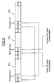
- the reference TP denotes a remote terminal such as a cellular mobile phone which is in communication with a base station.
- the mobile phone TP comprises a direct-conversion receiver DCR connected to an antenna ANT for receiving an incident signal.
- the direct-conversion receiver comprises an analogic stage connected to a digital stage or base band unit, BBU, through analog-to-digital converters AD.
- the analogic stage comprises a low-noise amplifier LNA and two processing pathes including mixers MX, conventional low path filters LPF and programmable gain amplification means PGA.
- the two mixers MX receive respectively from a phase locked loop PLL two signals, having mutually phase difference of 90°. After frequency transposition in the mixers, the two processing pathes define respectively two streams I and Q as it is well known by the man skilled in the art. Because the receiver is a direct-conversion receiver, the receive signal is transposed in base band and then filtered and amplified at base band.
- the two digital streams I and Q are delivered to the base band unit BBU.
- This base band unit is well known by the man skilled in the art and comprises especially estimation channel means, demodulation means as well as source decoding means. Further, as it is also well known by the man skilled in the art, the gain of the programmable gain amplification means BGA is controlled by the base band unit.
- the direct-conversion receiver further comprises two compensation modules CMM. These compensation modules will compensate as it will be explained more in details thereafter, a static DC offset as well as an inventual dynamic DC offset.
- one compensation module is connected on the I processing path whereas the second compensation module is connected on the Q processing path.
- each compensation module is connected between the input BE of the analog-to-digital converters AD and one input of an adder SM, located on the processing path between the programmable gain amplification means PGA and the output of the mixer MX.
- the adder SM is located after the low path filter LPF but it could be also located between the mixer MX and the low path filter LPF.
- the compensation module CMM comprises a capacitor C fb , called « smoothing capacitor » connected to said entry point through the adder SM.
- the compensation module comprises threshold control means TCM for defining the values of two opposite thresholds VNEG and VPOS.
- VNEG is equal to -VPOS.
- a first comparator C1 receives the threshold VNEG on its positive input and the signal present at point BE on its negative input.
- a second comparator C2 receives the signal present at point BE on its positive input and receives the threshold VPOS on its negative input.
- This two comparators C1 and C2 form main comparison means and are adapted to compare the voltage present at point BE with said two opposite threshold VNEG and VPOS.
- the compensation module CMM comprises also intermediate capacitor means comprising a first intermediate capacitor C1 sw and a second intermediate capacitor C2 sw .
- the first and second intermediate capacitors are identical, each having a first terminal connected to the ground, and a second terminal.
- the compensation module comprises also an intermediate control module for charging or discharging intermediate capacitor means C1 sw , C2 sw , depending on the result of the comparison performing by the comparators C1 and C2.
- the intermediate control module comprises a first resistor R1 sw and a second resistor R2 sw .
- Each resistor has a first terminal connected to the ground, and a second terminal.
- the intermediate control module comprises also a first intermediate current source SC1 and a second intermediate current source SC2.
- the intermediate control module further comprises a first switching means SW1 controlled by the ouptut of the first comparator C1 for selectively connecting the second terminal of the first intermediate capacitor C1 sw to the first intermediate current source SC1 or to the second terminal of the first resistor R1 sw .
- the intermediate control module comprises also a second switching means SW2 controlled by the output of the second comparator C2 for selectively connecting the second terminal of the second intermediate capacitor C2 sw to the second intermediate current source SC2 or to the second terminal of the second resistor R2 sw .
- the compensation module comprises also an auxiliary comparison module formed by a first auxiliary comparator C10 and a second auxiliary comparator C20.
- the first auxiliary comparator C10 has one input connected to the second terminal of the first intermediate capacitor S1 sw and another input (here the negative input) connected to a reference voltage V sw .
- the second auxiliary comparator C20 has its positive input connected to the second terminal of the second intermediate capacitor C2 sw , and its negative input receiving the reference voltage V sw .
- the compensation module comprises a final control module including a first final current source SC10 adapted to charge the smoothing capacitor C fb and a second final current source SC20 adapted to discharge the smoothing capacitor C fb .
- This final control module further comprises first final switching means SW10 controlled by the ouptut of the first auxiliary comparator C10, and connected between the smoothing capacitor and the first final current source SC10.
- the final control module comprises also a second final switching means SW20 controlled by the output of this second auxiliary comparator C20 and connected between the smoothing capacitor C fb and the second final current source SC20.
- the transmission channel is timely subdivided into frames TRi (only three frames are represented on figure 3).
- Each frame comprises several times slot, for example 8 time slots.
- the transmission of the information between the base station and the phone is carried on the successive frames within one or more consecutive time-slots in each frame.
- one or more consecutive time-slots is allocated to the phone within each frame.
- the compensation of the offset is performed in two phases.
- the compensation module is adapted to have two states corresponding to these two phases.
- the compensation module is in its first state during a part of time slot SL0 preceding the allocated time slot SL1 and will cancell the static DC offset.
- the compensation module is in its second state and will compensate an eventual dynamic DC offset.
- the threshold control means TCM set the value of the positive threshold equal to the absolute value of the maximum acceptable static DC offset, for example 10 mvolts.
- the negative threshold VNEG is set to the opposite value, i.e. - 10 mvolts.
- the gain of the programmable amplification means PGA is set at its maximum level either directly by the base band unit or by the threshold control means according to an information given by the base band unit.
- the amplified DC offset present at poing BE is compared with the two threshold, VPOS and VNEG, and, if it is out of the range (VPOS, VNEG), then one of the two comparators C1 and C2 will force the charge of one of the intermediate capacitors C1 sw , C2 sw in order to close the switch SW10 for positive DC offset or the switch SW20 for negative DC offset, and to charge or discharge the smoothing capacitor C fb .
- the voltage across the smoothing capacitor is then added through the buffer BF to the signal present at the other input of the adder SM.
- the switches SW1 and SW2 allow to connect the intermediate capacitors C1 sw and C2 sw with the resistors R1 sw and R2 sw .
- these intermediate capacitors C1 sw and C2 sw are discharged.
- the voltage at the second terminal of each intermediate capacitor is lower than the reference voltage V sw . Consequently, the switches SW10 and SW20 are opened an the compensation module has no effect.
- the switch SW2 connects intermediate capacitor C2 with the intermediate current source SC2, thereby allowing the charge of capacitor C2 sw .
- the switch SW20 is closed allowing the discharge of the smoothing capacitor. Consequently, a negative voltage is added by the adder to the signal present in the processing path.
- the two threshold VPOS and VNEG are propertly set by the threshold control means TCM according to the information coming from the base band unit.
- VPOS and VNEG are directly related to the information controlling the gain of the PGA.
- the threshold control means are adapted to set the values of the threshold at a percentage of the RMS value of the signal present at the input of analog-to-digital stages.
- the threshold control means TCM use the power information of the signal received during the allocated time-slot of the preceding frame, in order to obtain the RMS value of the signal.
- this RMS value obtained from a power information occuring during the preceeding allocated time-slot is used during the current allocated time-slot.
- the values of the threshold are chosen such that the DC offset is always lower than 35% of the RMS value of the received signal which fits the bare requirements of the GSM-DCS standard.
- each intermediate capacitor C1 sw or C2 sw needs a predetermined duration T chosen for example around 5 ⁇ s, in order to have a voltage across said intermediate capacitor equal to the reference voltage V sw .
- the stored charge of the smoothing capacitor C fb remains at least until the end of the allocated slot. So, in that case, no other compensation is required as the offset is lower than the threshold.
- the sign of the input of the adder SM receiving the offset compensation provided by the compensation module may be negative depending on which inputs of comparators C1 and C2 are connected to the point BE.
- the adder SM could be a substractor.
Priority Applications (1)
| Application Number | Priority Date | Filing Date | Title |
|---|---|---|---|
| EP01121636A EP1294151A1 (fr) | 2001-09-12 | 2001-09-12 | Suppression du décalage de composante continue pour un récepteur à conversion directe |
Applications Claiming Priority (1)
| Application Number | Priority Date | Filing Date | Title |
|---|---|---|---|
| EP01121636A EP1294151A1 (fr) | 2001-09-12 | 2001-09-12 | Suppression du décalage de composante continue pour un récepteur à conversion directe |
Publications (1)
| Publication Number | Publication Date |
|---|---|
| EP1294151A1 true EP1294151A1 (fr) | 2003-03-19 |
Family
ID=8178598
Family Applications (1)
| Application Number | Title | Priority Date | Filing Date |
|---|---|---|---|
| EP01121636A Withdrawn EP1294151A1 (fr) | 2001-09-12 | 2001-09-12 | Suppression du décalage de composante continue pour un récepteur à conversion directe |
Country Status (1)
| Country | Link |
|---|---|
| EP (1) | EP1294151A1 (fr) |
Cited By (6)
| Publication number | Priority date | Publication date | Assignee | Title |
|---|---|---|---|---|
| WO2005101671A2 (fr) | 2004-04-13 | 2005-10-27 | Maxlinear, Inc. | Procede et appareil pour supprimer le glissement de frequence de double conversion |
| KR100856769B1 (ko) * | 2004-02-20 | 2008-09-05 | 후지쯔 가부시끼가이샤 | Dc 오프셋 보정을 위한 다단 증폭기 및 dc 오프셋 보정 방법 |
| US8285240B2 (en) | 2004-12-10 | 2012-10-09 | Maxlinear, Inc. | Harmonic reject receiver architecture and mixer |
| US8306157B2 (en) | 2004-10-12 | 2012-11-06 | Maxlinear, Inc. | Receiver architecture with digitally generated intermediate frequency |
| US8311156B2 (en) | 2004-10-12 | 2012-11-13 | Maxlinear, Inc. | Hybrid receiver architecture using upconversion followed by direct downconversion |
| US8396173B2 (en) | 2007-10-01 | 2013-03-12 | Maxlinear, Inc. | I/Q calibration techniques |
Citations (3)
| Publication number | Priority date | Publication date | Assignee | Title |
|---|---|---|---|---|
| US5898912A (en) * | 1996-07-01 | 1999-04-27 | Motorola, Inc. | Direct current (DC) offset compensation method and apparatus |
| WO2000033458A1 (fr) * | 1998-11-30 | 2000-06-08 | Conexant Systems, Inc. | Recepteur pour signaux rf |
| EP1102413A2 (fr) * | 1999-11-15 | 2001-05-23 | Hitachi, Ltd. | Appareil de communication mobile et multibande |
-
2001
- 2001-09-12 EP EP01121636A patent/EP1294151A1/fr not_active Withdrawn
Patent Citations (3)
| Publication number | Priority date | Publication date | Assignee | Title |
|---|---|---|---|---|
| US5898912A (en) * | 1996-07-01 | 1999-04-27 | Motorola, Inc. | Direct current (DC) offset compensation method and apparatus |
| WO2000033458A1 (fr) * | 1998-11-30 | 2000-06-08 | Conexant Systems, Inc. | Recepteur pour signaux rf |
| EP1102413A2 (fr) * | 1999-11-15 | 2001-05-23 | Hitachi, Ltd. | Appareil de communication mobile et multibande |
Non-Patent Citations (1)
| Title |
|---|
| ABIDI A A: "DIRECT-CONVERSION RADIO TRANSCEIVERS FOR DIGITAL COMMUNICATIONS", IEEE JOURNAL OF SOLID-STATE CIRCUITS, IEEE INC. NEW YORK, US, vol. 30, no. 12, 1 December 1995 (1995-12-01), pages 1399 - 1410, XP000557245, ISSN: 0018-9200 * |
Cited By (11)
| Publication number | Priority date | Publication date | Assignee | Title |
|---|---|---|---|---|
| KR100856769B1 (ko) * | 2004-02-20 | 2008-09-05 | 후지쯔 가부시끼가이샤 | Dc 오프셋 보정을 위한 다단 증폭기 및 dc 오프셋 보정 방법 |
| WO2005101671A2 (fr) | 2004-04-13 | 2005-10-27 | Maxlinear, Inc. | Procede et appareil pour supprimer le glissement de frequence de double conversion |
| WO2005101671A3 (fr) * | 2004-04-13 | 2006-01-12 | Maxlinear Inc | Procede et appareil pour supprimer le glissement de frequence de double conversion |
| US7532870B2 (en) | 2004-04-13 | 2009-05-12 | Maxlinear, Inc. | Method and apparatus for DC offset removal |
| US7778613B2 (en) | 2004-04-13 | 2010-08-17 | Maxlinear, Inc. | Dual conversion receiver with programmable intermediate frequency and channel selection |
| US8718584B2 (en) | 2004-04-13 | 2014-05-06 | Maxlinear, Inc. | Dual conversion receiver with programmable intermediate frequency and channel selection |
| US8306157B2 (en) | 2004-10-12 | 2012-11-06 | Maxlinear, Inc. | Receiver architecture with digitally generated intermediate frequency |
| US8311156B2 (en) | 2004-10-12 | 2012-11-13 | Maxlinear, Inc. | Hybrid receiver architecture using upconversion followed by direct downconversion |
| US8285240B2 (en) | 2004-12-10 | 2012-10-09 | Maxlinear, Inc. | Harmonic reject receiver architecture and mixer |
| US8396173B2 (en) | 2007-10-01 | 2013-03-12 | Maxlinear, Inc. | I/Q calibration techniques |
| US9680674B2 (en) | 2007-10-01 | 2017-06-13 | Maxlinear, Inc. | I/Q calibration techniques |
Similar Documents
| Publication | Publication Date | Title |
|---|---|---|
| US6775530B2 (en) | Direct conversion of narrow-band RF signals | |
| FI112740B (fi) | Menetelmä ja laite automaattisen vahvistuksen ohjaukseen ja DC-offsetin poistamiseen kvadratuurivastaanottimessa | |
| US6442380B1 (en) | Automatic gain control in a zero intermediate frequency radio device | |
| US7110732B2 (en) | Subsampling RF receiver architecture | |
| US7593491B1 (en) | Quadrature single-mixer multi-mode radio frequency receiver | |
| US6757340B1 (en) | Radio receiver and method for preloading an average DC-offset into a channel filter | |
| US20040002318A1 (en) | Apparatus and method for calibrating image rejection in radio frequency circuitry | |
| KR20080058437A (ko) | 가변 이득 주파수 체배기 | |
| EP1212840A1 (fr) | Emetteur-recepteur multibande a capacite multifentes | |
| US6370133B1 (en) | CDMA receiver and method of operation | |
| US7095997B2 (en) | Direct-conversion receiver for a communication system using a modulation with non-constant envelope | |
| EP1257061A2 (fr) | Terminal d'usager et système sans fil avec circuit d'écrêtage du signal pour les convertisseurs analogiques-numériques du type sigma-delta à capacitées commutées | |
| EP1294151A1 (fr) | Suppression du décalage de composante continue pour un récepteur à conversion directe | |
| US7310386B2 (en) | Radio receiver utilizing a single analog to digital converter | |
| US20080152054A1 (en) | Interferer diversity | |
| US7082287B2 (en) | Radio communication system, received signal strength indicator compensating method for radio communication system, and base station/terminal station for radio communication system | |
| US6912381B2 (en) | Processing received signals | |
| US6977978B1 (en) | Adaptive channel filtration for communications systems | |
| US7248649B2 (en) | Digital baseband receiver including a time domain compensation module for suppressing group delay variation distortion incurred due to analog low pass filter deficiencies | |
| US8432940B2 (en) | Communication system over a power line distribution network | |
| WO2001063791A2 (fr) | Circuit emetteur-recepteur | |
| KR100717964B1 (ko) | 전류 혼합 방식을 이용한 i/q 변조기 및 이를 이용한직접 변환 방식 무선 통신 송신기 | |
| KR100282805B1 (ko) | 무선가입자망 시스템의 아이 및 큐 기저대역 신호변조시 캐리어 억압회로 | |
| Liu et al. | RF transceiver requirements and architectures for TD-SCDMA UE | |
| Manaï et al. | A CMOS switched capacitor channel select filter for direct conversion UMTS receiver |
Legal Events
| Date | Code | Title | Description |
|---|---|---|---|
| PUAI | Public reference made under article 153(3) epc to a published international application that has entered the european phase |
Free format text: ORIGINAL CODE: 0009012 |
|
| AK | Designated contracting states |
Kind code of ref document: A1 Designated state(s): AT BE CH CY DE DK ES FI FR GB GR IE IT LI LU MC NL PT SE TR Designated state(s): AT BE CH CY DE DK ES FI FR GB GR IE IT LI LU MC NL PT SE TR |
|
| AX | Request for extension of the european patent |
Extension state: AL LT LV MK RO SI |
|
| AKX | Designation fees paid | ||
| REG | Reference to a national code |
Ref country code: DE Ref legal event code: 8566 |
|
| STAA | Information on the status of an ep patent application or granted ep patent |
Free format text: STATUS: THE APPLICATION IS DEEMED TO BE WITHDRAWN |
|
| 18D | Application deemed to be withdrawn |
Effective date: 20030920 |