EP1294088A2 - Schaltungsanordnung zur Gleichrichtung eines Signals - Google Patents
Schaltungsanordnung zur Gleichrichtung eines Signals Download PDFInfo
- Publication number
- EP1294088A2 EP1294088A2 EP02102225A EP02102225A EP1294088A2 EP 1294088 A2 EP1294088 A2 EP 1294088A2 EP 02102225 A EP02102225 A EP 02102225A EP 02102225 A EP02102225 A EP 02102225A EP 1294088 A2 EP1294088 A2 EP 1294088A2
- Authority
- EP
- European Patent Office
- Prior art keywords
- circuit
- signal
- circuit arrangement
- transconductors
- output
- Prior art date
- Legal status (The legal status is an assumption and is not a legal conclusion. Google has not performed a legal analysis and makes no representation as to the accuracy of the status listed.)
- Granted
Links
Images

Classifications
-
- H—ELECTRICITY
- H02—GENERATION; CONVERSION OR DISTRIBUTION OF ELECTRIC POWER
- H02M—APPARATUS FOR CONVERSION BETWEEN AC AND AC, BETWEEN AC AND DC, OR BETWEEN DC AND DC, AND FOR USE WITH MAINS OR SIMILAR POWER SUPPLY SYSTEMS; CONVERSION OF DC OR AC INPUT POWER INTO SURGE OUTPUT POWER; CONTROL OR REGULATION THEREOF
- H02M7/00—Conversion of AC power input into DC power output; Conversion of DC power input into AC power output
- H02M7/02—Conversion of AC power input into DC power output without possibility of reversal
- H02M7/04—Conversion of AC power input into DC power output without possibility of reversal by static converters
- H02M7/12—Conversion of AC power input into DC power output without possibility of reversal by static converters using discharge tubes with control electrode or semiconductor devices with control electrode
- H02M7/21—Conversion of AC power input into DC power output without possibility of reversal by static converters using discharge tubes with control electrode or semiconductor devices with control electrode using devices of a triode or transistor type requiring continuous application of a control signal
- H02M7/217—Conversion of AC power input into DC power output without possibility of reversal by static converters using discharge tubes with control electrode or semiconductor devices with control electrode using devices of a triode or transistor type requiring continuous application of a control signal using semiconductor devices only
Definitions
- the invention relates to a circuit arrangement for rectifying a signal, where two transconductors with the signal to be rectified in phase opposition are controllable.
- the object of the present invention is to provide a circuit arrangement for Propose rectification of a signal, which over a wide range Frequency range works precisely and provides a linear output signal.
- This object is achieved in that the outputs of the transconductors via a first diode with a first switching point and each a second diode with the second polarity opposite to the first are connected that the circuit points to a predetermined potential are connected and that at least one of the circuit points is rectified Signal can be removed.
- the circuit arrangement according to the invention is basically for both differential signals, i.e. signals that are in pairs in opposite phase, as well as for signals effective against ground are suitable.
- the opposite phase when driving the Transconductors can be achieved by using two phase signals are fed in the same direction inputs of the transconductors or that in-phase signals fed to opposite inputs of both transconductors become.
- the specified potential can be selected by the person skilled in the art in such a way that on the basis of this, modulation in both directions is possible, the predetermined one Potential in the middle of the modulation range of the transconductors lies.
- the given potential for the first and to select the second switching point such that a clean transition between the Diodes done.
- the rectified signal as a voltage signal in an advantageous manner can be obtained in that at least one of the circuit points via a Current input of a current / voltage converter with the specified potential is connected, the output of which forms the output of the circuit arrangement. there it is preferably provided that the current / voltage converter from a current mirror circuit is formed.
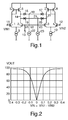
- the exemplary embodiments according to FIGS. 1, 3 and 4 each consist of two Transconductors.
- a first transconductor contains a differential amplifier that is formed by transistors 1, 2 and a current source 9, and a current mirror circuit from transistors 5 and 6.
- a second Transconductor consisting of transistors 3, 4, a current source 10 and others Transistors 7, 8 built.
- the person skilled in the art can also use the transconductors realize other suitable reinforcing components, such as Field effect transistors or tubes.
- the derivative is a Voltage output signal not shown in detail to the basic To explain the function of the circuit arrangement according to the invention.
- the signal to be rectified is used in the exemplary embodiments according to FIGS. 1 and 3 fed via inputs 11 and 12 to the base connections of transistors 1 and 4.
- the base connections of transistors 2 and 3 are at a reference potential V1, which is fed in at 13.
- the amplified signals can the outputs 14, 15 of the Transconductors are removed. These outputs are each via a diode 16, 17 with a first node 18 and one opposite each other polarized diode 19, 20 connected to a second node 21.
- circuit points 18, 21 are each constant Potential V2, V3, which is indicated by the DC voltage symbols 22 and 23 is indicated. Circuit details to achieve a constant Potentials are known per se and need in connection with the circuit arrangement according to the invention not to be explained.
- the rectified signal is thus present as a current signal.
- the Signal is guaranteed in both directions that from the output 14, 15 one Current can flow into the voltage sources 22, 23.
- V2, V3 within the output characteristic of the transconductors are one linear gain and linear rectification are thus ensured, in particular also because the transistors 6, 7 are not controlled to saturation.
- the illustration clearly shows that even for very small amplitudes around the zero point, a linear characteristic curve is present. Depending on the linearity requirements, such a Circuit arrangement then up to output amplitudes of 40%, 60% or 70% operate.
- a Current / voltage converter which acts as a current mirror circuit with transistors 24, 25 and a load resistor 27 is formed.
- the connection 26 is a predetermined one Supply potential that corresponds approximately to the potential V2 (Fig. 1).
- the output signal of the circuit arrangement according to FIG. 2 lies - in contrast to that rectified input signal - not as a differential signal, but as a signal before mass. Should a differential signal for further processing are required, the circuit arrangement according to FIG. 3 by one at the Switching point 18 connected further current / voltage converter added become.
- a further resistor 29 is provided for reasons of symmetry. Also here a further output, not shown, can be derived from node 18 become.
- the circuit arrangement according to FIG. 4 is for a input signal effective against ground. This is via the entrance 11 supplied to the transistors 1, 3, while the base connections of the transistors 2, 4 lie on the reference potential V1, which is fed to an input 13.
Landscapes
- Engineering & Computer Science (AREA)
- Power Engineering (AREA)
- Rectifiers (AREA)
- Amplifiers (AREA)
- Measurement Of Current Or Voltage (AREA)
- Burglar Alarm Systems (AREA)
- Electrophonic Musical Instruments (AREA)
Abstract
Description
Claims (4)
- Schaltungsanordnung zur Gleichrichtung eines Signals, wobei zwei Transkonduktoren mit dem gleichzurichtenden Signal gegenphasig ansteuerbar sind,
dadurch gekennzeichnet, dass die Ausgänge der Transkonduktoren (1 bis 10) über je eine erste Diode (16, 17) mit einem ersten Schaltungspunkt (18) und über je eine zweite, zur ersten entgegengesetzt gepolte Diode (19, 20) mit einem zweiten Schaltungspunkt (21) verbunden sind, dass die Schaltungspunkte an ein vorgegebenes Potential angeschlossen sind und dass mindestens einem der Schaltungspunkte ein gleichgerichtetes Signal entnehmbar ist. - Schaltungsanordnung nach Anspruch 1,
dadurch gekennzeichnet, dass mindestens einer der Schaltungspunkte (21) über einen Stromeingang eines Strom/Spannungswandlers (24, 25, 27) mit dem vorgegebenen Potential verbunden ist, dessen Ausgang den Ausgang der Schaltungsanordnung bildet. - Schaltungsanordnung nach Anspruch 1,
dadurch gekennzeichnet, dass der Strom/Spannungswandler von einer Stromspiegelschaltung (24, 25) gebildet ist. - Schaltungsanordnung nach Anspruch 1,
dadurch gekennzeichnet, dass mindestens einer der Schaltungspunkte (18, 21) über einen Widerstand (29, 30) an das vorgegebene Potential angeschlossen ist und einen Ausgang (31) der Schaltungsanordnung bildet.
Applications Claiming Priority (2)
| Application Number | Priority Date | Filing Date | Title |
|---|---|---|---|
| DE10142022A DE10142022A1 (de) | 2001-08-28 | 2001-08-28 | Schaltungsanordnung zur Gleichrichtung eines Signals |
| DE10142022 | 2001-08-28 |
Publications (3)
| Publication Number | Publication Date |
|---|---|
| EP1294088A2 true EP1294088A2 (de) | 2003-03-19 |
| EP1294088A3 EP1294088A3 (de) | 2005-01-26 |
| EP1294088B1 EP1294088B1 (de) | 2011-04-20 |
Family
ID=7696812
Family Applications (1)
| Application Number | Title | Priority Date | Filing Date |
|---|---|---|---|
| EP02102225A Expired - Lifetime EP1294088B1 (de) | 2001-08-28 | 2002-08-28 | Schaltungsanordnung zur Gleichrichtung eines Signals |
Country Status (5)
| Country | Link |
|---|---|
| US (1) | US6703886B2 (de) |
| EP (1) | EP1294088B1 (de) |
| JP (1) | JP4108416B2 (de) |
| AT (1) | ATE506738T1 (de) |
| DE (2) | DE10142022A1 (de) |
Family Cites Families (8)
| Publication number | Priority date | Publication date | Assignee | Title |
|---|---|---|---|---|
| US3353106A (en) * | 1964-05-28 | 1967-11-14 | Gen Electric | Automatic variable threshold control circuit |
| NL7508771A (nl) * | 1975-07-23 | 1977-01-25 | Philips Nv | Gelijkrichtschakeling. |
| US4219745A (en) * | 1978-06-15 | 1980-08-26 | The United States Of America As Represented By The Secretary Of The Air Force | Backlash filter apparatus |
| US4187537A (en) * | 1978-12-21 | 1980-02-05 | Zenith Radio Corporation | Full-wave rectifier |
| DE3012823A1 (de) * | 1980-04-02 | 1981-10-08 | Licentia Patent-Verwaltungs-Gmbh, 6000 Frankfurt | Doppelweggleichrichterschaltung |
| US4360866A (en) * | 1980-12-29 | 1982-11-23 | Motorola, Inc. | Linear full wave rectifier and method for providing full wave rectified signals |
| DE4316027A1 (de) * | 1993-05-13 | 1994-11-17 | Telefunken Microelectron | Schaltungsanordnung zum Gleichrichten von Wechselspannungssignalen |
| JP2908282B2 (ja) * | 1995-05-22 | 1999-06-21 | 日本電気移動通信株式会社 | 両波整流回路 |
-
2001
- 2001-08-28 DE DE10142022A patent/DE10142022A1/de not_active Withdrawn
-
2002
- 2002-08-23 US US10/227,205 patent/US6703886B2/en not_active Expired - Fee Related
- 2002-08-23 JP JP2002243899A patent/JP4108416B2/ja not_active Expired - Fee Related
- 2002-08-28 EP EP02102225A patent/EP1294088B1/de not_active Expired - Lifetime
- 2002-08-28 AT AT02102225T patent/ATE506738T1/de active
- 2002-08-28 DE DE50215009T patent/DE50215009D1/de not_active Expired - Lifetime
Also Published As
| Publication number | Publication date |
|---|---|
| ATE506738T1 (de) | 2011-05-15 |
| JP4108416B2 (ja) | 2008-06-25 |
| JP2003143859A (ja) | 2003-05-16 |
| US6703886B2 (en) | 2004-03-09 |
| US20030042964A1 (en) | 2003-03-06 |
| EP1294088A3 (de) | 2005-01-26 |
| DE10142022A1 (de) | 2003-03-20 |
| EP1294088B1 (de) | 2011-04-20 |
| DE50215009D1 (de) | 2011-06-01 |
Similar Documents
| Publication | Publication Date | Title |
|---|---|---|
| EP0087175B1 (de) | Schaltung zur elektronischen Verstärkungsstellung | |
| DE10020933B4 (de) | ASK-Modulator und Kommunikationsgerät mit einem ASK-Modulator | |
| DE1901804B2 (de) | Stabilisierter differentialverstaerker | |
| EP0073929A2 (de) | Integrierbare signalverarbeitende Halbleiterschaltung | |
| DE69814558T2 (de) | Verstärker mit hohem Verstärkungsgrad und begrenzter Ausgangsdynamik | |
| DE2702022B2 (de) | Verstärkerschaltung | |
| DE69514417T2 (de) | Differenzverstärker | |
| DE69403739T2 (de) | Spannung-Strom-Umsetzter | |
| DE1122109B (de) | Schaltung zur Amplitudenmodulation von mit Halbeiterelementen bestueckten Sendern | |
| DE2826536C2 (de) | Schaltungsanordnung zur erdfreien Übertragung von Signalen über Trennstellen in Fernmeldeanlagen | |
| EP1294088B1 (de) | Schaltungsanordnung zur Gleichrichtung eines Signals | |
| DE3007715A1 (de) | Verstaerkerschaltung mit durch eine steuerspannung steuerbarer gesamtverstaerkung | |
| DE2617873C2 (de) | FM-Diskriminator | |
| DE3008469A1 (de) | Schaltungsanordnung zur abgabe eines fuer die groesse eines eingangssignals kennzeichnenden signals an eine anzeigeeinrichtung | |
| DE2142817A1 (de) | Verstarker mit veränderlichem Ver starkungsfaktor | |
| DE10134450A1 (de) | Umschaltbare Stromquelle | |
| DE19518225C1 (de) | Schaltungsanordnung zur Bildung der Quadratwurzel eines Eingangssignals | |
| DE1762420A1 (de) | Elektronischer Schalter mit Feldeffekttransistor | |
| DE2154700A1 (de) | Fernsteuerbarer, elektronischer Differentialwiderstand | |
| EP0586730B1 (de) | Schaltungsanordnung zum Umformen eines symmetrischen gegenphasigen Eingangssignales in ein unsymmetrisches einphasiges Ausgangssignal | |
| DE3012823C2 (de) | ||
| DE3331200C2 (de) | ||
| DE3633415C2 (de) | ||
| EP0162525A2 (de) | Schaltungsanordnung zur Verringerung der Verzerrungen bei einem FM-Quadraturdemodulator | |
| DE1512749C (de) | Verstarker mit Gegentakteingang und Ein tak tausgang |
Legal Events
| Date | Code | Title | Description |
|---|---|---|---|
| PUAI | Public reference made under article 153(3) epc to a published international application that has entered the european phase |
Free format text: ORIGINAL CODE: 0009012 |
|
| AK | Designated contracting states |
Kind code of ref document: A2 Designated state(s): AT BE BG CH CY CZ DE DK EE ES FI FR GB GR IE IT LI LU MC NL PT SE SK TR |
|
| AX | Request for extension of the european patent |
Extension state: AL LT LV MK RO SI |
|
| RAP1 | Party data changed (applicant data changed or rights of an application transferred) |
Owner name: KONINKLIJKE PHILIPS ELECTRONICS N.V. Owner name: PHILIPS INTELLECTUAL PROPERTY & STANDARDS GMBH |
|
| PUAL | Search report despatched |
Free format text: ORIGINAL CODE: 0009013 |
|
| AK | Designated contracting states |
Kind code of ref document: A3 Designated state(s): AT BE BG CH CY CZ DE DK EE ES FI FR GB GR IE IT LI LU MC NL PT SE SK TR |
|
| AX | Request for extension of the european patent |
Extension state: AL LT LV MK RO SI |
|
| 17P | Request for examination filed |
Effective date: 20050726 |
|
| AKX | Designation fees paid |
Designated state(s): AT BE BG CH CY CZ DE DK EE ES FI FR GB GR IE IT LI LU MC NL PT SE SK TR |
|
| RAP1 | Party data changed (applicant data changed or rights of an application transferred) |
Owner name: NXP B.V. |
|
| GRAP | Despatch of communication of intention to grant a patent |
Free format text: ORIGINAL CODE: EPIDOSNIGR1 |
|
| GRAS | Grant fee paid |
Free format text: ORIGINAL CODE: EPIDOSNIGR3 |
|
| GRAA | (expected) grant |
Free format text: ORIGINAL CODE: 0009210 |
|
| AK | Designated contracting states |
Kind code of ref document: B1 Designated state(s): AT BE BG CH CY CZ DE DK EE ES FI FR GB GR IE IT LI LU MC NL PT SE SK TR |
|
| REG | Reference to a national code |
Ref country code: GB Ref legal event code: FG4D Free format text: NOT ENGLISH |
|
| REG | Reference to a national code |
Ref country code: CH Ref legal event code: EP |
|
| REG | Reference to a national code |
Ref country code: IE Ref legal event code: FG4D Free format text: LANGUAGE OF EP DOCUMENT: GERMAN |
|
| REF | Corresponds to: |
Ref document number: 50215009 Country of ref document: DE Date of ref document: 20110601 Kind code of ref document: P |
|
| REG | Reference to a national code |
Ref country code: DE Ref legal event code: R096 Ref document number: 50215009 Country of ref document: DE Effective date: 20110601 |
|
| REG | Reference to a national code |
Ref country code: NL Ref legal event code: VDEP Effective date: 20110420 |
|
| PG25 | Lapsed in a contracting state [announced via postgrant information from national office to epo] |
Ref country code: SE Free format text: LAPSE BECAUSE OF FAILURE TO SUBMIT A TRANSLATION OF THE DESCRIPTION OR TO PAY THE FEE WITHIN THE PRESCRIBED TIME-LIMIT Effective date: 20110420 Ref country code: PT Free format text: LAPSE BECAUSE OF FAILURE TO SUBMIT A TRANSLATION OF THE DESCRIPTION OR TO PAY THE FEE WITHIN THE PRESCRIBED TIME-LIMIT Effective date: 20110822 |
|
| REG | Reference to a national code |
Ref country code: IE Ref legal event code: FD4D |
|
| PG25 | Lapsed in a contracting state [announced via postgrant information from national office to epo] |
Ref country code: ES Free format text: LAPSE BECAUSE OF FAILURE TO SUBMIT A TRANSLATION OF THE DESCRIPTION OR TO PAY THE FEE WITHIN THE PRESCRIBED TIME-LIMIT Effective date: 20110731 Ref country code: FI Free format text: LAPSE BECAUSE OF FAILURE TO SUBMIT A TRANSLATION OF THE DESCRIPTION OR TO PAY THE FEE WITHIN THE PRESCRIBED TIME-LIMIT Effective date: 20110420 Ref country code: GR Free format text: LAPSE BECAUSE OF FAILURE TO SUBMIT A TRANSLATION OF THE DESCRIPTION OR TO PAY THE FEE WITHIN THE PRESCRIBED TIME-LIMIT Effective date: 20110721 Ref country code: CY Free format text: LAPSE BECAUSE OF FAILURE TO SUBMIT A TRANSLATION OF THE DESCRIPTION OR TO PAY THE FEE WITHIN THE PRESCRIBED TIME-LIMIT Effective date: 20110420 |
|
| PG25 | Lapsed in a contracting state [announced via postgrant information from national office to epo] |
Ref country code: NL Free format text: LAPSE BECAUSE OF FAILURE TO SUBMIT A TRANSLATION OF THE DESCRIPTION OR TO PAY THE FEE WITHIN THE PRESCRIBED TIME-LIMIT Effective date: 20110420 |
|
| PG25 | Lapsed in a contracting state [announced via postgrant information from national office to epo] |
Ref country code: CZ Free format text: LAPSE BECAUSE OF FAILURE TO SUBMIT A TRANSLATION OF THE DESCRIPTION OR TO PAY THE FEE WITHIN THE PRESCRIBED TIME-LIMIT Effective date: 20110420 Ref country code: IE Free format text: LAPSE BECAUSE OF FAILURE TO SUBMIT A TRANSLATION OF THE DESCRIPTION OR TO PAY THE FEE WITHIN THE PRESCRIBED TIME-LIMIT Effective date: 20110420 Ref country code: EE Free format text: LAPSE BECAUSE OF FAILURE TO SUBMIT A TRANSLATION OF THE DESCRIPTION OR TO PAY THE FEE WITHIN THE PRESCRIBED TIME-LIMIT Effective date: 20110420 |
|
| PLBE | No opposition filed within time limit |
Free format text: ORIGINAL CODE: 0009261 |
|
| STAA | Information on the status of an ep patent application or granted ep patent |
Free format text: STATUS: NO OPPOSITION FILED WITHIN TIME LIMIT |
|
| BERE | Be: lapsed |
Owner name: NXP B.V. Effective date: 20110831 |
|
| PG25 | Lapsed in a contracting state [announced via postgrant information from national office to epo] |
Ref country code: SK Free format text: LAPSE BECAUSE OF FAILURE TO SUBMIT A TRANSLATION OF THE DESCRIPTION OR TO PAY THE FEE WITHIN THE PRESCRIBED TIME-LIMIT Effective date: 20110420 Ref country code: DK Free format text: LAPSE BECAUSE OF FAILURE TO SUBMIT A TRANSLATION OF THE DESCRIPTION OR TO PAY THE FEE WITHIN THE PRESCRIBED TIME-LIMIT Effective date: 20110420 |
|
| 26N | No opposition filed |
Effective date: 20120123 |
|
| PG25 | Lapsed in a contracting state [announced via postgrant information from national office to epo] |
Ref country code: MC Free format text: LAPSE BECAUSE OF NON-PAYMENT OF DUE FEES Effective date: 20110831 |
|
| REG | Reference to a national code |
Ref country code: CH Ref legal event code: PL |
|
| PG25 | Lapsed in a contracting state [announced via postgrant information from national office to epo] |
Ref country code: LI Free format text: LAPSE BECAUSE OF NON-PAYMENT OF DUE FEES Effective date: 20110831 Ref country code: CH Free format text: LAPSE BECAUSE OF NON-PAYMENT OF DUE FEES Effective date: 20110831 |
|
| REG | Reference to a national code |
Ref country code: DE Ref legal event code: R097 Ref document number: 50215009 Country of ref document: DE Effective date: 20120123 |
|
| PG25 | Lapsed in a contracting state [announced via postgrant information from national office to epo] |
Ref country code: IT Free format text: LAPSE BECAUSE OF FAILURE TO SUBMIT A TRANSLATION OF THE DESCRIPTION OR TO PAY THE FEE WITHIN THE PRESCRIBED TIME-LIMIT Effective date: 20110420 Ref country code: BE Free format text: LAPSE BECAUSE OF NON-PAYMENT OF DUE FEES Effective date: 20110831 |
|
| REG | Reference to a national code |
Ref country code: AT Ref legal event code: MM01 Ref document number: 506738 Country of ref document: AT Kind code of ref document: T Effective date: 20110828 |
|
| PG25 | Lapsed in a contracting state [announced via postgrant information from national office to epo] |
Ref country code: AT Free format text: LAPSE BECAUSE OF NON-PAYMENT OF DUE FEES Effective date: 20110828 |
|
| PG25 | Lapsed in a contracting state [announced via postgrant information from national office to epo] |
Ref country code: LU Free format text: LAPSE BECAUSE OF NON-PAYMENT OF DUE FEES Effective date: 20110828 |
|
| PG25 | Lapsed in a contracting state [announced via postgrant information from national office to epo] |
Ref country code: BG Free format text: LAPSE BECAUSE OF FAILURE TO SUBMIT A TRANSLATION OF THE DESCRIPTION OR TO PAY THE FEE WITHIN THE PRESCRIBED TIME-LIMIT Effective date: 20110720 |
|
| PG25 | Lapsed in a contracting state [announced via postgrant information from national office to epo] |
Ref country code: TR Free format text: LAPSE BECAUSE OF FAILURE TO SUBMIT A TRANSLATION OF THE DESCRIPTION OR TO PAY THE FEE WITHIN THE PRESCRIBED TIME-LIMIT Effective date: 20110420 |
|
| REG | Reference to a national code |
Ref country code: DE Ref legal event code: R084 Ref document number: 50215009 Country of ref document: DE |
|
| PGFP | Annual fee paid to national office [announced via postgrant information from national office to epo] |
Ref country code: DE Payment date: 20140722 Year of fee payment: 13 |
|
| REG | Reference to a national code |
Ref country code: DE Ref legal event code: R084 Ref document number: 50215009 Country of ref document: DE Effective date: 20141015 |
|
| PGFP | Annual fee paid to national office [announced via postgrant information from national office to epo] |
Ref country code: FR Payment date: 20140822 Year of fee payment: 13 Ref country code: GB Payment date: 20140725 Year of fee payment: 13 |
|
| REG | Reference to a national code |
Ref country code: DE Ref legal event code: R119 Ref document number: 50215009 Country of ref document: DE |
|
| GBPC | Gb: european patent ceased through non-payment of renewal fee |
Effective date: 20150828 |
|
| REG | Reference to a national code |
Ref country code: FR Ref legal event code: ST Effective date: 20160429 |
|
| PG25 | Lapsed in a contracting state [announced via postgrant information from national office to epo] |
Ref country code: GB Free format text: LAPSE BECAUSE OF NON-PAYMENT OF DUE FEES Effective date: 20150828 Ref country code: DE Free format text: LAPSE BECAUSE OF NON-PAYMENT OF DUE FEES Effective date: 20160301 |
|
| PG25 | Lapsed in a contracting state [announced via postgrant information from national office to epo] |
Ref country code: FR Free format text: LAPSE BECAUSE OF NON-PAYMENT OF DUE FEES Effective date: 20150831 |