EP1293985A1 - Data backup device and step-up/step-down power supply - Google Patents
Data backup device and step-up/step-down power supply Download PDFInfo
- Publication number
- EP1293985A1 EP1293985A1 EP00935591A EP00935591A EP1293985A1 EP 1293985 A1 EP1293985 A1 EP 1293985A1 EP 00935591 A EP00935591 A EP 00935591A EP 00935591 A EP00935591 A EP 00935591A EP 1293985 A1 EP1293985 A1 EP 1293985A1
- Authority
- EP
- European Patent Office
- Prior art keywords
- power supply
- voltage
- control means
- data backup
- main power
- Prior art date
- Legal status (The legal status is an assumption and is not a legal conclusion. Google has not performed a legal analysis and makes no representation as to the accuracy of the status listed.)
- Granted
Links
Images
Classifications
-
- G—PHYSICS
- G11—INFORMATION STORAGE
- G11C—STATIC STORES
- G11C11/00—Digital stores characterised by the use of particular electric or magnetic storage elements; Storage elements therefor
- G11C11/21—Digital stores characterised by the use of particular electric or magnetic storage elements; Storage elements therefor using electric elements
- G11C11/34—Digital stores characterised by the use of particular electric or magnetic storage elements; Storage elements therefor using electric elements using semiconductor devices
- G11C11/40—Digital stores characterised by the use of particular electric or magnetic storage elements; Storage elements therefor using electric elements using semiconductor devices using transistors
- G11C11/401—Digital stores characterised by the use of particular electric or magnetic storage elements; Storage elements therefor using electric elements using semiconductor devices using transistors forming cells needing refreshing or charge regeneration, i.e. dynamic cells
- G11C11/4063—Auxiliary circuits, e.g. for addressing, decoding, driving, writing, sensing or timing
- G11C11/407—Auxiliary circuits, e.g. for addressing, decoding, driving, writing, sensing or timing for memory cells of the field-effect type
- G11C11/4074—Power supply or voltage generation circuits, e.g. bias voltage generators, substrate voltage generators, back-up power, power control circuits
-
- G—PHYSICS
- G11—INFORMATION STORAGE
- G11C—STATIC STORES
- G11C11/00—Digital stores characterised by the use of particular electric or magnetic storage elements; Storage elements therefor
- G11C11/21—Digital stores characterised by the use of particular electric or magnetic storage elements; Storage elements therefor using electric elements
- G11C11/34—Digital stores characterised by the use of particular electric or magnetic storage elements; Storage elements therefor using electric elements using semiconductor devices
- G11C11/40—Digital stores characterised by the use of particular electric or magnetic storage elements; Storage elements therefor using electric elements using semiconductor devices using transistors
- G11C11/401—Digital stores characterised by the use of particular electric or magnetic storage elements; Storage elements therefor using electric elements using semiconductor devices using transistors forming cells needing refreshing or charge regeneration, i.e. dynamic cells
- G11C11/406—Management or control of the refreshing or charge-regeneration cycles
-
- G—PHYSICS
- G11—INFORMATION STORAGE
- G11C—STATIC STORES
- G11C5/00—Details of stores covered by group G11C11/00
- G11C5/14—Power supply arrangements, e.g. power down, chip selection or deselection, layout of wirings or power grids, or multiple supply levels
- G11C5/141—Battery and back-up supplies
-
- G—PHYSICS
- G11—INFORMATION STORAGE
- G11C—STATIC STORES
- G11C5/00—Details of stores covered by group G11C11/00
- G11C5/14—Power supply arrangements, e.g. power down, chip selection or deselection, layout of wirings or power grids, or multiple supply levels
- G11C5/147—Voltage reference generators, voltage or current regulators; Internally lowered supply levels; Compensation for voltage drops
Definitions
- This invention relates to a data backup apparatus for backing up data by controlling power fed to a memory, and a step-up/down power supply for feeding power to on-vehicle equipments, e.g., a car navigation device, and so on.
- on-vehicle equipments e.g., a car navigation device, and so on.
- an SRAM, a rewritable ROM or the like is installed therein, and data in an on-vehicle equipment such as a car navigation device is saved in the SRAM or the like.
- the conventional data backup apparatus Since the conventional data backup apparatus is constructed as mentioned above, it requires a large amount of data, such as map information on the surroundings, to be read from an external memory or the like, at the time of starting the on-vehicle equipment. Thus, there has been such an inevitable problem in the conventional art that a considerable time is required before the on-vehicle equipment starts its actual operation.
- the present invention has been made to solve the foregoing problems, and it is an object of the invention to provide a data backup apparatus capable of saving a large amount of data inside an on-vehicle equipment.
- a data backup apparatus comprising: control means for changing a dynamic RAM to a self-refresh mode when detection means detects an OFF command of a main power supply, and feeding power from a backup power supply to the dynamic RAM.
- power is fed from the main power supply to the dynamic RAM during the period from the detection of the OFF command of the main power supply to the completion of the changing to the self-refresh mode.
- a memory area that receives power from the backup power supply is designated, and power is fed only to the thus designated memory area.
- information regarding the memory area to receive power from the backup power supply is indicated.
- the feeding of power from the main power supply to a predetermined equipment is stopped, when the output voltage of the main power supply is reduced.
- the control means and the SDRAM are kept separated from each other until the initial setting of the control means is completed.
- a step-up/down power supply comprising: a step-up DC/DC converter for outputting a predetermined voltage by stepping up a voltage applied from a main power supply when the applied voltage drops below a reference voltage.
- the predetermined voltage can be applied to an on-vehicle equipment even if a cranking operation or the like causes a reduction in the voltage applied from the main power supply, it is possible to stably operate the on-vehicle equipment.
- a voltage signal is captured from an outputting stage for outputting a predetermined voltage, so as to activate a switching element of the step-up DC/DC converter.
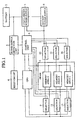
- Fig. 1 is a schematic diagram showing a data backup apparatus according to a first embodiment of the invention.
- a reference numeral 1 denotes a dynamic RAM (DRAM) for storing the data of an on-vehicle equipment such as a car navigation device, and the DRAM includes a plurality of memory areas A to C.
- DRAM dynamic RAM
- a reference numeral 2 denotes a battery (main power supply) installed in a vehicle; 3 a step-up/down power supply that receives a voltage applied from the battery 2 and outputs a predetermined voltage even if fluctuation occurs in the applied voltage; and 4 a backup power supply.
- a reference numeral 5 denotes a power supply detection unit (detection means) for detecting an ON/OFF command or the like of the battery 2; 6 a reset circuit for initializing a CPU 7 when the power supply detection unit 5 detects the ON command; 7 a CPU for changing the DRAM 1 to a self-refresh mode when the power supply detection unit 5 detects the OFF command; 8 a control unit for switching the power supply source of the DRAM 1 from the step-up/down power supply 3 to the backup power supply 4 when the DRAM 1 is shifted to the self-refresh mode; and numerals 9 to 14 denote selectors.
- the CPU7, the control unit 8 and the selectors 9 to 14 constitute a control means.
- step-up/down power supply 3 When the switch of a vehicle key is in an ACC or ON position, power is fed from the battery 2 to the step-up/down power supply 3. From the step-up/down power supply 3, power is fed to the CPU 7 and the DRAM 1. The specific operation of the step-up/down power supply 3 will be described later.
- the CPU7 can perform various data processing operations (if it is a CPU for a navigation device, the CPU 7 can execute route searching, map displaying and so on), and stores data regarding such processing in the DRAM 1.
- the power supply detection unit 5 detects a power supply OFF command, and notifies the detection to the CPU 7.
- the CPU 7 Upon receiving the OFF command from the power supply detection unit 5, the CPU 7 sets the DRAM 1 into the self-refresh mode to prevent the loss of data stored in the DRAM 1.
- the DRAM 1 since the same data must be written at regular intervals to continuously hold the data in the DRAM 1, the DRAM 1 is changed to the mode of repeating automatic data writing (self-refresh mode). If the DRAM 1 is an SDRAM, when a CKE terminal is at "H”, control from an external unit is accepted. On the other hand, when the CKE terminal is at "L”, the previous mode is maintained. Thus, the DRAM 1 is changed to the self-refresh mode before the CKE terminal is changed from "H” to "L".
- control unit 8 switches the power supply source of the DRAM 1 from the step-up/down power supply 3 to the backup power supply 4.
- the DRAM 1 receives power fed from the backup power supply 4 even if the output voltage of the battery 2 drops, data can be held continuously.
- the power supply detection unit 5 detects a power supply ON command, and notifies the detection to the reset circuit 6.
- the reset circuit 6 Upon receiving the ON command from the power supply detection unit 5, the reset circuit 6 initializes the CPU 7, and the CPU 7 releases the self refresh mode.
- the control unit 8 disconnects the CPU 7 and the DRAM from each other during the initialization of the CPU 7 to prevent the destruction or the like of the data stored in the DRAM 1. After the completion of the initialization of the CPU 7, the control unit 8 connects the CPU 7 and the DRAM 1 with each other, and switches the power supply source of the DRAM 1 from the backup power supply 4 to the step-up/down power supply 3.
- the DRAM 1 when the power supply detection unit 5 detects the OFF command of the battery 2, the DRAM 1 is set to the self-refresh mode, and power is fed from the backup power supply 4 to the DRAM 1.
- the DRAM 1 When the power supply detection unit 5 detects the OFF command of the battery 2, the DRAM 1 is set to the self-refresh mode, and power is fed from the backup power supply 4 to the DRAM 1.
- a large amount of data can be saved in the DRAM 1 low in price and large in capacity. Therefore, for example, if an on-vehicle equipment is a navigation device, not only the present position information but surrounding map information and additional information can also be backed up, so that the device can be set to a usable state almost instantaneously when it is actuated at the next time
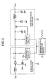
- Fig. 2 is a schematic diagram showing a step-up/down power supply according to a second embodiment of the invention.
- a reference 21 denotes a reference wave generation circuit
- 22 a step-up DC/DC converter for applying a predetermined voltage V1 by stepping up a voltage V IN applied from the battery 2 when the applied voltage V IN drops below a reference voltage
- 23 a step-down DC/DC converter connected in series to the step-up DC/DC converter 22, and adapted to apply a predetermined voltage V OUT by stepping down a voltage V IN applied from the battery 2 when the applied voltage V IN rises above the reference voltage.
- cranking is carried out by actuating a self-starting motor.
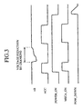
- the cranking operation causes a reduction in the output voltage of the battery 2 (see “+B" in Fig. 3)
- an operable voltage for the CPU 7 or the DRAM 1 cannot be secured.
- the data stored in the DRAM 1 may be lost, and other problems may occur.
- the step-up/down power supply 3 is provided to secure operable voltages for the CPU 7 and the DRAM 1 even if the output voltage of the battery 2 is reduced by the cranking operation.
- the step-up/down power supply 3 includes: a step-up DC/DC converter 22 for applying a predetermined voltage V1 by stepping up a voltage V IN applied from the battery 2 when the voltage V IN drops below the reference voltage; and a step-down DC/DC converter 23 for applying a predetermined voltage V OUT by stepping down a voltage V IN applied from the battery 2 when the voltage V IN raises above the reference voltage.
- the step-up DC/DC converter 22 is designed to hardly operate in the operating voltage region of the step-down DC/DC converter 23; and the step-down DC/DC converter 23 to hardly operate in the operating voltage region of the step-up DC/DC converter 22. Accordingly, by individually operating the converters, conversion efficiency can be increased.
- the control circuit 22a of the step-up DC/DC converter 22 captures a voltage signal from an output stage X that outputs a predetermined voltage V1, and activates a MOS-FET 22b as a switching device. Accordingly, even if the voltage V IN applied from the battery 2 drops below the operable voltage of MOS-FET 22b, a proper operable voltage can be secured for the MOS-FET 22b. As a result, it is possible to continue a stepping-up operation.
- step-up/down power supply for outputting a predetermined voltage irrespective of fluctuation in the applied voltage
- a fly-back type converter using a transformer.
- convertible power is decided depending on the capacity of the transformer.
- the size of the transformer was a bottleneck, making it difficult to construct a large-capacity step-up/down power supply.
- the step-up/down power supply 3 shown in Fig. 2 since a choke coil is used instead of the transformer, a mounting area can be designed to be small with respect to a power supply capacity.
- the step-up DC/DC converter 22 is provided for applying a predetermined voltage V1 by stepping up a voltage V IN applied from the battery 2 when the voltage V IN drops below the reference voltage, a predetermined voltage can be applied to the on-vehicle equipment even if a cranking operation or the like causes a reduction in the output voltage of the battery 2, making it possible to stably operate the on-vehicle equipment. Therefore, since the resetting of the navigation device or the like can be prevented at the time of starting the engine, it is also possible to apply the step-up/down power supply to a car in an idling stop state.
- the power supply source of the DRAM 1 is switched from the step-up/down power supply 3 to the backup power supply 4.
- the CPU 7 designates one memory area among a plurality of memory areas A to C, which receives power from the backup power supply 4 (e.g., in the case where there is data stored in the memory area A while no data have been stored in the memory areas B and C, only the memory area A is set to receive power by controlling the selectors 9 and 10), and the control unit 8 provides power only to the thus designated memory area.
- the foregoing third embodiment has been explained as to the case where a memory area that can receive power from the backup power supply 4 is designated, and only the thus designated memory area can be provided with power.
- a backup verification mechanism for indicating information regarding the memory area designated to receive power from the backup power supply 4 may be provided on the memory map of the CPU 7.
- the foregoing first embodiment has been explained as to the case in which the step-up/down power supply 3 was provided for securing the operable voltage of the CPU 7 or the DRAM 1 even if a reduction in the output voltage of the battery 2 is caused due to the cranking operation.
- it can be arranged such that when a reduction occurs in the output voltage of the battery 2, the feeding of power from the battery 2 to a certain equipment is stopped.
- the data backup apparatus of the invention is suitable for backing up a large amount of data by properly feeding power to the large-capacity dynamic RAM installed in the on-vehicle equipment.
- the step-up/down power supply of the invention is suitable for stably operating an on-vehicle equipment by applying a predetermined voltage to the on-vehicle equipment even when fluctuation occurs in a voltage applied from the main power supply such as a battery.
Landscapes
- Engineering & Computer Science (AREA)
- Power Engineering (AREA)
- Microelectronics & Electronic Packaging (AREA)
- Computer Hardware Design (AREA)
- Power Sources (AREA)
- Techniques For Improving Reliability Of Storages (AREA)
- Dram (AREA)
Abstract
Description
Claims (8)
- A data backup apparatus, comprising:a dynamic RAM (1) for storing data;detection means for detecting an OFF command of a main power supply (2); andcontrol means (8) for changing said dynamic RAM to a self-refresh mode when said detection means detects the OFF command of the main power supply, and feeding power from a backup power supply (4) to said dynamic RAM.
- The data backup apparatus according to claim 1, wherein said control means (8) makes the dynamic RAM (1) supplied with power from the main power supply (2) during the period from the detection of the OFF command of the main power supply to completion of the changing to the self refresh mode.
- The data backup apparatus according to claim 1, wherein said control means (8) designates one memory area that receives power from the backup power supply among a plurality of memory areas (A,B,C) constituting said dynamic RAM (1), and feeds power only to the thus designated memory area.
- The data backup apparatus according to claim 3, wherein said control means (8) indicates information regarding the memory area that receives power from the backup power supply (4).
- The data backup apparatus according to claim 1, wherein said control means (8) stops feeding of power from the main power supply (2) to a predetermined equipment, when an output voltage of the main power supply (2) in reduced.
- The data backup apparatus according to claim 1, wherein if an SDRAM is used as the dynamic RAM (1), said control means and said SDRAM are kept separated from each other until initial setting of said control means is completed.
- A step-up/down power supply comprising:a step-up DC/DC converter (22) for outputting a predetermined voltage by stepping up a voltage applied from a main power supply when the applied voltage drops below a reference voltage; anda step-down DC/DC converter (23) connected in series with said step-up DC/DC converter (22), and adapted to output apredetermined voltage by stepping down the voltage applied from the main power supply (2) when the applied voltage rises above the reference voltage.
- A step-up/down power supply according to claim 7,
characterized in that said step-up DC/DC converter (22) captures a voltage signal from outputting means for outputting a predetermined voltage, and drives a switching device (22b).
Applications Claiming Priority (1)
| Application Number | Priority Date | Filing Date | Title |
|---|---|---|---|
| PCT/JP2000/003732 WO2001095335A1 (en) | 2000-06-08 | 2000-06-08 | Data backup device and step-up/step-down power supply |
Publications (3)
| Publication Number | Publication Date |
|---|---|
| EP1293985A1 true EP1293985A1 (en) | 2003-03-19 |
| EP1293985A4 EP1293985A4 (en) | 2005-11-02 |
| EP1293985B1 EP1293985B1 (en) | 2007-08-15 |
Family
ID=11736130
Family Applications (1)
| Application Number | Title | Priority Date | Filing Date |
|---|---|---|---|
| EP00935591A Expired - Lifetime EP1293985B1 (en) | 2000-06-08 | 2000-06-08 | Data backup device and step-up/step-down power supply |
Country Status (4)
| Country | Link |
|---|---|
| US (1) | US6731563B1 (en) |
| EP (1) | EP1293985B1 (en) |
| DE (1) | DE60036026T2 (en) |
| WO (1) | WO2001095335A1 (en) |
Families Citing this family (7)
| Publication number | Priority date | Publication date | Assignee | Title |
|---|---|---|---|---|
| TW591393B (en) * | 2003-01-22 | 2004-06-11 | Fujitsu Ltd | Memory controller |
| US7493441B2 (en) * | 2005-03-15 | 2009-02-17 | Dot Hill Systems Corporation | Mass storage controller with apparatus and method for extending battery backup time by selectively providing battery power to volatile memory banks not storing critical data |
| JP4501868B2 (en) * | 2006-02-17 | 2010-07-14 | 村田機械株式会社 | Memory system control method |
| JP2010233380A (en) * | 2009-03-27 | 2010-10-14 | Seiko Epson Corp | Power supply circuit and electronic device |
| JP5397609B2 (en) | 2009-09-01 | 2014-01-22 | 日本電気株式会社 | Disk array device |
| JP2011059937A (en) * | 2009-09-09 | 2011-03-24 | Seiko Epson Corp | Electronic device |
| WO2016069022A1 (en) * | 2014-10-31 | 2016-05-06 | Hewlett Packard Enterprise Development Lp | Shared backup power self-refresh mode |
Family Cites Families (31)
| Publication number | Priority date | Publication date | Assignee | Title |
|---|---|---|---|---|
| US4316248A (en) * | 1978-12-06 | 1982-02-16 | Data General Corporation | Memory refresh means including means for providing refresh addresses during power failures |
| JPS55105891A (en) * | 1979-01-30 | 1980-08-13 | Sharp Corp | Refresh system for dynamic memory |
| JPS56101691A (en) * | 1980-01-14 | 1981-08-14 | Toshiba Corp | Refresh control system |
| JPS56110117A (en) * | 1980-02-04 | 1981-09-01 | Toshiba Corp | Electric power supply backup system of electronic computer |
| DE3242952A1 (en) * | 1982-11-20 | 1984-05-24 | SWF-Spezialfabrik für Autozubehör Gustav Rau GmbH, 7120 Bietigheim-Bissingen | CALCULATOR, ESPECIALLY ON-BOARD CALCULATOR FOR MOTOR VEHICLES |
| JPS6275072A (en) | 1985-09-26 | 1987-04-06 | Kawasaki Heavy Ind Ltd | Regulating method for ignition timing of two-cycle engine |
| JPS62286143A (en) * | 1986-06-04 | 1987-12-12 | Oki Electric Ind Co Ltd | Semiconductor memory device |
| US4979171A (en) * | 1989-05-03 | 1990-12-18 | Rockwell International Corporation | Announcement and tone code generator for telephonic network and method |
| US5430681A (en) * | 1989-05-08 | 1995-07-04 | Hitachi Maxell, Ltd. | Memory cartridge and its memory control method |
| JP2898016B2 (en) * | 1989-06-23 | 1999-05-31 | 新日本製鐵株式会社 | Memory device |
| JPH04111295A (en) * | 1990-08-30 | 1992-04-13 | Matsushita Electric Ind Co Ltd | Memory control circuit |
| JPH04295238A (en) | 1991-03-20 | 1992-10-20 | Nec Corp | Backup power supply circuit |
| JPH0528757A (en) * | 1991-07-18 | 1993-02-05 | Canon Inc | Memory control circuit |
| JPH0591734A (en) | 1991-09-25 | 1993-04-09 | Matsushita Electric Ind Co Ltd | Chopper converter DCDC converter |
| JPH065823A (en) * | 1992-06-19 | 1994-01-14 | Toshiba Corp | Nonvolatile semiconductor memory device and method of using the same |
| JPH0767326A (en) | 1993-08-26 | 1995-03-10 | Matsushita Electric Works Ltd | Power supply device |
| JP3416215B2 (en) * | 1993-08-31 | 2003-06-16 | キヤノン株式会社 | Facsimile machine |
| JPH07334432A (en) * | 1994-06-07 | 1995-12-22 | Hitachi Ltd | Memory control circuit |
| JP3747381B2 (en) * | 1994-11-10 | 2006-02-22 | 富士通株式会社 | Power supply control circuit for electronic devices with built-in batteries |
| JP3302847B2 (en) * | 1994-12-02 | 2002-07-15 | 富士通株式会社 | Storage device |
| JPH099613A (en) * | 1995-06-14 | 1997-01-10 | Fujitsu Ltd | DC-DC converter |
| US5659208A (en) * | 1995-07-14 | 1997-08-19 | International Business Machines Corporation | Power supply with multiple isolated regulators and isolation mode |
| US5860125A (en) * | 1995-11-08 | 1999-01-12 | Advanced Micro Devices, Inc. | Integrated circuit including a real time clock, configuration RAM, and memory controller in a core section which receives an asynchronous partial reset and an asynchronous master reset |
| JPH10105478A (en) * | 1996-09-30 | 1998-04-24 | Nec Eng Ltd | Memory control circuit |
| JPH1115742A (en) * | 1997-06-19 | 1999-01-22 | Kofu Nippon Denki Kk | Memory refresh control circuit |
| JPH11144455A (en) * | 1997-11-12 | 1999-05-28 | Canon Inc | Memory backup control device and memory backup control method |
| JP4136076B2 (en) * | 1998-06-04 | 2008-08-20 | キヤノン株式会社 | Memory backup control device and memory backup control method |
| US6084813A (en) * | 1998-06-04 | 2000-07-04 | Canon Kabushiki Kaisha | Apparatus and method for controlling memory backup using main power supply and backup power supply |
| US6088762A (en) * | 1998-06-19 | 2000-07-11 | Intel Corporation | Power failure mode for a memory controller |
| US6317657B1 (en) * | 1998-08-18 | 2001-11-13 | International Business Machines Corporation | Method to battery back up SDRAM data on power failure |
| JP4056173B2 (en) * | 1999-04-14 | 2008-03-05 | 富士通株式会社 | Semiconductor memory device and method for refreshing semiconductor memory device |
-
2000
- 2000-06-08 DE DE60036026T patent/DE60036026T2/en not_active Expired - Lifetime
- 2000-06-08 EP EP00935591A patent/EP1293985B1/en not_active Expired - Lifetime
- 2000-06-08 WO PCT/JP2000/003732 patent/WO2001095335A1/en not_active Ceased
- 2000-06-08 US US10/031,118 patent/US6731563B1/en not_active Expired - Lifetime
Also Published As
| Publication number | Publication date |
|---|---|
| WO2001095335A1 (en) | 2001-12-13 |
| DE60036026D1 (en) | 2007-09-27 |
| US6731563B1 (en) | 2004-05-04 |
| EP1293985A4 (en) | 2005-11-02 |
| DE60036026T2 (en) | 2008-04-30 |
| EP1293985B1 (en) | 2007-08-15 |
Similar Documents
| Publication | Publication Date | Title |
|---|---|---|
| KR100545131B1 (en) | Control system | |
| EP0081593A1 (en) | Vehicular power source system | |
| US11011788B2 (en) | Standby state maintaining device | |
| US20080276050A1 (en) | Erase handling method for non-volatile memory and electronic apparatus thereof | |
| US6731563B1 (en) | Data backup device and step-up/step-down power supply | |
| EP1346880B1 (en) | Vehicle-mounted information device | |
| EP2312419A1 (en) | Power supply control device, image forming apparatus, and method of controlling power supply | |
| JP2001322515A (en) | Method and apparatus for reducing dark current for vehicles | |
| JPH0764872A (en) | Data storage controller | |
| JP4135510B2 (en) | Electronic control device and program | |
| JP2019185398A (en) | On-vehicle device | |
| JP4655398B2 (en) | Vehicle control device with backup function | |
| JP2725560B2 (en) | Nonvolatile semiconductor memory device | |
| JPH07114401A (en) | RAM backup circuit | |
| JP3159816B2 (en) | Nonvolatile semiconductor memory device | |
| JP2001341595A (en) | Power source control device | |
| JPH09330104A (en) | Electronic control system for automobile | |
| JP2009181624A (en) | Nonvolatile semiconductor memory device | |
| JPH05265881A (en) | Write protecting circuit of and write protecting method for non-volatile memory | |
| JPH1082342A (en) | Vehicle control device | |
| JP2004062406A (en) | In-vehicle control network device | |
| JP2001322513A (en) | Method and apparatus for reducing dark current for vehicles | |
| JP2008089612A (en) | Reception device and reception control method | |
| JPH0336125Y2 (en) | ||
| JPH0736631A (en) | Storage device |
Legal Events
| Date | Code | Title | Description |
|---|---|---|---|
| PUAI | Public reference made under article 153(3) epc to a published international application that has entered the european phase |
Free format text: ORIGINAL CODE: 0009012 |
|
| 17P | Request for examination filed |
Effective date: 20020207 |
|
| AK | Designated contracting states |
Kind code of ref document: A1 Designated state(s): AT BE CH CY DE DK ES FI FR GB GR IE IT LI LU MC NL PT SE |
|
| RBV | Designated contracting states (corrected) |
Designated state(s): DE |
|
| RIC1 | Information provided on ipc code assigned before grant |
Ipc: 7G 11C 11/401 A Ipc: 7G 11C 11/406 B |
|
| RIC1 | Information provided on ipc code assigned before grant |
Ipc: 7G 06F 1/32 B Ipc: 7G 11C 11/406 B Ipc: 7G 11C 11/401 A |
|
| A4 | Supplementary search report drawn up and despatched |
Effective date: 20050914 |
|
| RAP1 | Party data changed (applicant data changed or rights of an application transferred) |
Owner name: MITSUBISHI DENKI KABUSHIKI KAISHA |
|
| 17Q | First examination report despatched |
Effective date: 20051229 |
|
| GRAP | Despatch of communication of intention to grant a patent |
Free format text: ORIGINAL CODE: EPIDOSNIGR1 |
|
| GRAS | Grant fee paid |
Free format text: ORIGINAL CODE: EPIDOSNIGR3 |
|
| GRAA | (expected) grant |
Free format text: ORIGINAL CODE: 0009210 |
|
| AK | Designated contracting states |
Kind code of ref document: B1 Designated state(s): DE |
|
| REF | Corresponds to: |
Ref document number: 60036026 Country of ref document: DE Date of ref document: 20070927 Kind code of ref document: P |
|
| PLBE | No opposition filed within time limit |
Free format text: ORIGINAL CODE: 0009261 |
|
| STAA | Information on the status of an ep patent application or granted ep patent |
Free format text: STATUS: NO OPPOSITION FILED WITHIN TIME LIMIT |
|
| 26N | No opposition filed |
Effective date: 20080516 |
|
| REG | Reference to a national code |
Ref country code: DE Ref legal event code: R084 Ref document number: 60036026 Country of ref document: DE Effective date: 20110706 Ref country code: DE Ref legal event code: R084 Ref document number: 60036026 Country of ref document: DE Effective date: 20110506 |
|
| PGFP | Annual fee paid to national office [announced via postgrant information from national office to epo] |
Ref country code: DE Payment date: 20160601 Year of fee payment: 17 |
|
| REG | Reference to a national code |
Ref country code: DE Ref legal event code: R119 Ref document number: 60036026 Country of ref document: DE |
|
| PG25 | Lapsed in a contracting state [announced via postgrant information from national office to epo] |
Ref country code: DE Free format text: LAPSE BECAUSE OF NON-PAYMENT OF DUE FEES Effective date: 20180103 |