This invention relates to a synchronous
semiconductor memory device. More specifically, this
invention relates to a high-speed random-cycle
synchronous semiconductor memory (FCRAM) which has the
function of reading and writing data from and into the
memory cell array at random at high speeds and which is
used in, for example, a high-speed-cycle synchronous
FCRAM (SDR-FCRAM) or a double-data-rate synchronous
FCRAM (DDR-FCRAM) that realizes twice the data transfer
rate of an SDR-FCRAM.
Conventional synchronous DRAMS (SDRAMs) are such
that they make the data access speed of DRAMs (dynamic
random-access memories) as fast as SRAMs (static
random-access memories) and enable a greater data
bandwidth (the number of data bytes per unit time) at a
higher clock frequency. SDRAMs have been put to
practical use since the 4-Mbit/16-Mbit DRAM
generations. In the 64-Mbit DRAM generation, most of
the DRAMs now in use are SDRAMs.
Recently, an attempt has been made to make the
data transfer rate of SDRAMs much faster. For example,
double-data-rate SDRAMs (DDR-SDRAMs) that operate at a
data transfer rate twice that of conventional
equivalents have been proposed and are now being
commercialized.
Although being faster in the data transfer rate,
or being improved in the bandwidth, SDRAMs have the
following problem: it is difficult to access the cell
data in the memory core at higher speed. The reason
for this is that, in the case of SDRAMs, the data
access from a different row address as a result of the
change of the row access requires a destructive read
operation unique to DRAMs and an amplify operation and
that it also requires a specific length of time (or
core latency) for a precharge operation preceding the
next core access. Therefore, it is difficult to
radically speed up the core cycle time (or random cycle
time tRC).
To solve this problem, a Fast Cycle RAM (FCRAM)
has been proposed which performs a core access
operation and a precharge operation in a pipeline
manner, thereby decreasing the random cycle time tRC to
less than 1/2 that of a conventional SDRAM (for
example, see "a 20-ns Random Access Pipelined Operation
DRAM," VLSI Symp. 1998). In recent years, products
using such an FCRAM are going to be commercialized in
the field of networks that transfer random data at high
speeds, centering on LAN switches and routers, which
have used SRAMs up to now.
Here, the command system including the basic
operations of FCRAMs will be explained briefly (for
further details, see, for example, Japanese Patent
Application No. 11-373531 (Jpn. Pat. Appln. KOKAI
Publication No. 2001-189077).
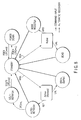
FIG. 8 shows how the state of FCRAM changes
according to a command input. In FIG. 8, the way the
command input is determined by a combination of a first
command and a second command is illustrated.
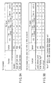
FIGS. 9A and 9B show the relationship between the
commands in FIG. 8 and pin inputs corresponding to the
commands (in function tables).
In the FCRAM, two pins, a chip select (/CS) pin
and a function control (FN = row address strobe/RAS)
pin, are generally allocated as external terminals for
inputting commands for controlling internal circuit
operations. It is impossible to determine many command
inputs by using only the two pins. To overcome this
problem, combining a first command and a second command
enables a plurality of commands to be determined by
only the two pins, the /CS pin and the FN pin.
In FIG. 8, a write active command WRA (Write with
Auto-close) and a read active command RDA (Read with
Auto-close) are first commands. A lower address latch
command LAL (Lower Address Latch), a mode register set
command MRS (Mode Register Set), and an auto refresh
command REF (Auto Refresh) are second commands.
As shown in FIG. 9A, as for the first commands,
when the input level of the /CS pin is low and the
input level of the FN pin is high, a read active
command RDA is set as a command input. In addition,
when the input level of the /CS pin is low and the
input level of the FN pin is low, a write active
command WRA is set as a command input. As shown in
FIG. 9B, as for second commands, when the input level
of the /CS pin is high, a lower address latch command
LAL is set as a command input. Moreover, when the
input level of the /CS pin is low, a mode register set
command MRS and an auto refresh command REF are set as
command inputs.
Specifically, as shown in FIG. 8, when each of a
first command and a second command is inputted in the
wait state (STANDBY), a read active command RDA or a
write active command WRA is given directly. In this
case, as seen from the tables shown in FIGS. 9A and 9B,
the input of a command is accepted when the input level
of the /CS pin is made low. The distinction between a
read command and a write command is made according to
the level of the input supplied to the FN pin. In this
example, if the command is a read command, the FN pin
is set high. If the command is a write command, the FN
pin is set low.
Furthermore, a first command can be used to give a
row address for sense amplifier division decoding.
There is a limit to the number of pins of a package.
Thus, some of the existing control pins are used as
address pins, thereby suppressing an increase in the
number of pins.
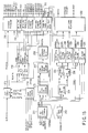
FIG. 10 shows the pin allocation of a double-data-rate
synchronous FCRAM (DDR-FCRAM) package some of whose
control pins are used as address pins, as compared with
the pin allocation of a DDR-SDRAM package. Explanation
will be given, taking a 66-pin TSOP (Thin Small Outline
Package) standardized in JEDEC (Joint Electron Devices
Engineering Council) as an example.
In the FCRAM in this example, the column address
strobe (/CAS) pin and write enable (/WE) pin of the
SDRAM are converted into address pins A13, A14. This
increases the number of sense amplifiers to be decoded,
preventing the number of sense amplifiers to be
activated from being limited.
An address taken in by a first command is called
an upper address UA and an address taken in by a second
command is called a lower address LA.
With the rising edge of a clock in a first
command, the upper address UA is taken in from the
address pins A13, A14 corresponding to the /WE pin and
/CAS pin and normal address pins A0 to A12. If the
first command is a read command, a word line WL is
selected according to the row address. Then, the data
from the memory cell MC connected to the selected word
line WL is read onto a bit line pair BLn, /BLn. The
read-out data is amplified by a bit-line sense
amplifier S/A. The input of the first command
completes the operations up to this point. In FIG. 10,
the /WE pin and /CAS pin change in level according to
the input of addresses. Moreover, the /RAS pin is
changed in level according to the FN input.
Next, after one clock cycle since the first
command was inputted, any one of a lower address latch
command LAL, a mode register set command MRS, and an
auto refresh command REF is inputted as a second
command.
The following is an explanation of a case where,
in the second command, the /CS pin is set high (command
LAL) and column addresses CA0 to CAj (lower addresses
LA) are taken in from address pins A0 to A14. In this
case, a column address is only taken in as the second
command. That is, the column select line CSL
corresponding to the column address is selected. In
this way, the data amplified by the bit-line sense
amplifier S/A is transferred to a data-line pair MDQ.
Then, the data is amplified again by a read buffer (or
secondary sense amplifier) DQRB. Finally, the data is
outputted at an output pin.
A command decoder for realizing the aforementioned
operations is composed of, for example, a controller, a
first-command decoder, and a second-command decoder as
shown in FIGS. 11 to 13. Specifically, FIG. 11 shows a
concrete configuration of a controller for controlling
the operation of the command decoder. FIG. 12 shows a
concrete configuration of an upper command decoder.
FIG. 13 shows a concrete configuration of a lower
command decoder.
A controller shown in FIG. 11 is composed of
inverters 101 to 111, clocked inverters 121 to 126,
NAND gates 131 to 134, and a NOR gate 141.
Specifically, an opposite-phase signal bCSIN obtained
by internally buffering the external signal from the
/CS pin is supplied to the input terminal of the
clocked inverter 121 controlled by a signal CLKIN
obtained by internally buffering an external clock
signal and its opposite-phase signal bCLKIN. The input
terminal of the inverter 101 is connected to the output
terminal of the clocked inverter 121.
The output terminal of the clocked inverter 122
controlled by signals CLKIN, bCLKIN is connected to the
input terminal of the inverter 101. The input terminal
of the clocked inverter 122 is connected to the output
terminal of the inverter 101.
The output terminal of the inverter 101 is
connected to one input terminal of the NOR gate 141 and
one input terminal of the NAND gate 131. The output
terminal of the inverter 103 is connected to the other
input terminal of the NOR gate 141. The output
terminal of the inverter 104 is connected to the other
input terminal of the NAND gate 131. The output
terminal of the inverter 103 is connected to the input
terminal of the inverter 104. The signal CLKIN is
supplied to the input terminal of the inverter 103.
The input terminal of the inverter 102 is
connected to the output terminal of the NOR gate 141.
The opposite-phase signal bCSLTC is outputted from the
output terminal of the inverter 102. The signal bCSLTC
is a signal obtained by internally buffering the
external input /CS and latching it for half a clock.
The input terminal of the inverter 105 is
connected to the output terminal of the NAND gate 131.
A signal NOPLTC is outputted from the output terminal
of the inverter 105.
On the other hand, a signal bCOLACTRU indicating
that a command RDA has been inputted is supplied to one
input terminal of each of NAND gates 132, 133. A
signal bCOLACTWU indicating that a command WRA has been
inputted is supplied to the other input terminal of
each of the NAND gates 132, 134.
The output terminal of the NAND gate 132 is
connected to the input terminal of the clocked inverter
123 controlled by signals bCLKIN, CLKIN. The input
terminal of the inverter 106 is connected to the output
terminal of the clocked inverter 123. The input
terminal of the clocked inverter 125 controlled by
signals CLKIN, bCLKIN is connected to the output
terminal of the inverter 106. The input terminal of
the inverter 107 is connected to the output terminal of
the clocked inverter 125. Three stages of inverters
108, 109, 110 are connected to the output terminal of
the inverter 107. An opposite-phase signal bACTUDSB is
outputted from the output terminal of the third-stage
inverter 110.
The output terminal of the clocked inverter 124
controlled by signals CLKIN, bCLKIN is connected to the
input terminal of the inverter 106. The input terminal
of the clocked inverter 124 is connected to the output
terminal of the inverter 106. The output terminal of
the clocked inverter 126 controlled by signals bCLKIN,
CLKIN is connected to the input terminal of the
inverter 107. The input terminal of the clocked
inverter 126 is connected to the output terminal of the
inverter 107.
The output terminal of the NAND gate 134 is
connected to the other input terminal of the NAND gate
133. The output terminal of the NAND gate 133 is
connected to one input terminal of the NAND gate 134.
A signal PCREAD is outputted from the output terminal
of the NAND gate 133. The output terminal of the NAND
gate 133 is connected to the input terminal of the
inverter 111. A signal PCWRITE is outputted from the
output terminal of the inverter 111.
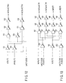
The upper command decoder shown in FIG. 12 is
composed of inverters 151 to 156, a NAND gate 161, and
a NOR gate 171. Specifically, the controller shown in
FIG. 11 supplies a signal bCSLTC to the input terminal
of the inverter 151. A signal bRASLTC is supplied to
the input terminal of the inverter 154. The signal
bRASLTC is a signal obtained by internally buffering an
external input /RAS(FN) and latching it for half a
clock.
The output terminal of the inverter 151 is
connected to a first input terminal of the NAND gate
161. The output terminal of the inverter 154 is
connected to a second input terminal of the NAND gate
161. The output terminal of the inverter 110 shown in
FIG. 11 is connected to a third input terminal of the
NAND gate 161. Then, a signal bACTUDSB is supplied
from the output terminal of the inverter 110.
The input terminal of the inverter 152 is
connected to the output terminal of the NAND gate 161.
The input terminal of the inverter 153 is connected to
the output terminal of the inverter 152. A signal
bCOLACTWU is outputted from the output terminal of the
inverter 153 and then supplied to the controller.
On the other hand, the output terminal of the
inverter 155 is connected to a first input terminal of
the NOR gate 171. The output terminal of the inverter
110 shown in FIG. 11 is connected to the input terminal
of the inverter 155. The output terminal of the
inverter 154 is connected to a second input terminal of
the NOR gate 171. The output terminal of the inverter
102 shown in FIG. 11 is connected to a third input
terminal of the NOR gate 171. Then, an opposite-phase
signal bCSLTC is supplied to the output terminal of the
inverter 102.
The input terminal of the inverter 156 is
connected to the output terminal of the NOR gate 171.
Then, an opposite-phase signal bCOLACTRU is outputted
from the output terminal of the inverter 156 and then
supplied to the controller.
The circuit of FIG. 12 is configured so as to
reduce the number of stages by receiving each signal
with the NOR gate 171. This makes the random access
time tRAC faster.
The lower command decoder shown in FIG. 13 is
composed of inverters 181 to 189, NAND gates 191 to
194, and NOR gates 201, 202. Specifically, the
controller shown in FIG. 11 supplies a signal NOPLTC to
one input terminal of each of the NAND gates 191, 192.
The controller of FIG. 11 supplies a signal bCSLTC to
the input terminal of the inverter 189. The output
terminal of the inverter 189 is connected to one input
terminal of each of the NAND gates 193, 194.
The controller of FIG. 11 supplies signal bACTUDSB
and signal PCWRITE to the corresponding input terminals
of the NOR gate 201. The output terminal of the NOR
gate 201 is connected to the other input terminal of
each of the NAND gates 191, 193.
The controller of FIG. 11 supplies signal bACTUDSB
and signal PCREAD to the corresponding input terminals
of the NOR gate 202. The output terminal of the NOR
gate 202 is connected to the other input terminal of
each of the NAND gates 192, 194.
The output terminal of the NAND gate 191 is
connected to the input terminal of the inverter 181.
The input terminal of the inverter 182 is connected to
the output terminal of the inverter 181. An opposite-phase
signal bCOLACTR is outputted from the output
terminal of the inverter 182. The signal bCOLACTR is a
signal that indicates a lower address latch command LAL
has been inputted in the clock cycle following a read
active command RDA.
The output terminal of the NAND gate 192 is
connected to the input terminal of the inverter 183.
The input terminal of the inverter 184 is connected to
the output terminal of the inverter 183. An opposite-phase
signal bCOLACTW is outputted from the output
terminal of the inverter 184. The signal bCOLACTW is a
signal that indicates a lower address latch command LAL
has been inputted in the clock cycle following a write
active command WRA.
The output terminal of the NAND gate 193 is
connected to the input terminal of the inverter 185.
The input terminal of the inverter 186 is connected to
the output terminal of the inverter 185. An
opposite-phase signal bMSET is outputted from the
output terminal of the inverter 186. The signal bMSET
is a signal that indicates a mode register set command
MRS has been inputted in the clock cycle following a
read active command RDA.
The output terminal of the NAND gate 194 is
connected to the input terminal of the inverter 187.
The input terminal of the inverter 188 is connected to
the output terminal of the inverter 187. An opposite-phase
signal bREFR is outputted from the output
terminal of the inverter 188. The signal bREFR is a
signal that indicates an auto refresh command REF has
been inputted in the clock cycle following a write
active command WRA.
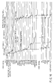
Next, the operations of the circuits shown in
FIGS. 11 to 13 will be explained by reference to a
timing chart shown in FIG. 14. When a first command is
inputted, signal bCSLTC and signal bRASLTC change
according to the potential VBCS of the /CS pin and the
potential VFN of the FN pin. Then, signal bCOLACTWU
(or, signal bCOLACTRU) goes low. At this time, the
corresponding one of signal PCWRITE or signal PCREAD in
the controller goes high.
Signal bACTUDSB goes low during only one clock
cycle starting with the falling of clock signal CLKIN
since a first command was inputted. This makes it
possible to accept the next second command.
A signal NOPLTC is a signal for sensing that
signal bCSIN goes high with the timing of the rising of
clock signal CLKIN, or that the mode is in NP (No
Operating). Thus, when a lower address latch command
LAL is inputted in inputting a second command, signal
NOPLTC goes high. Signal bCOLACTW goes low, when the
following three conditions are fulfilled: signal NOPLTC
is high, signal bACTUBSB is low, and signal PCWRITE is
high (= signal PCREAD is low). This makes it possible
to sense that a lower address latch command LAL has
been inputted, while discriminating between a read and
a write operation.
When an auto refresh command REF or a mode
register set command MRS is inputted in inputting a
second command, signal bCSLTC goes low. Whether the
command REF or MRS is inputted depends on whether the
first command is a write active command WRA or a read
active command RDA.
When signal bACTUDSB goes low, signal bREFR and
signal bMSET go low, depending on the state of signal
FCREAD/FCWRITE. In this case, since the /CS pin is at
the low level, a first-command command decoder
operates. To prevent the command decoder from
operating, signal bACTUDSB is inputted at the same
time.
The aforementioned operations produce the effects
shown in the following items (A) and (B).
Therefore, it is possible to take in a row address and
simultaneously start not only the operation of
peripheral circuits but also the operation of the
memory core. This makes the start of random access
earlier than the determination of the start of the
memory core from the second command. That is, random
access time tRAC is. made one cycle earlier
automatically. (B) A first command determines read/write.
Therefore, in a second command, only a lower address LA
is taken in. As a result, the time from when a column
select line CSL is selected until the data is outputted
becomes shorter than before. This makes random access
time tRAC faster. Moreover, the transfer of the data
to a peripheral circuit can be finished earlier. This
enables the precharge operation of bit lines BL, bBL to
be brought forward after the word line WL is reset.
That is, it is possible to make faster not only random
access time tRAC but also random cycle time tRC.
What has been explained is about the basic
operation of the command system of the FCRAM. As
described above, a first command determines read/write.
The RAS restore operation of the core, the selection of
column select lines CSL, and the RAS precharge
operation are carried out in a pipeline manner. This
makes the random cycle time tRC equal to or less than
1/2 that of a conventional equivalent. The realization
of the pipeline operation makes the FCRAM different
greatly from a conventional SDRAM/DDR-SDRAM.
FIG. 15 shows a system configuration of the ROW
control circuit of the FCRAM that performs RAS restore
operations, the selection of column select lines CSL,
and RAS precharge operations in a pipeline manner.
The ROW control circuit of the FCRAM includes a
bank active controller 211, a bank timer 212, an upper
address driver 213, an upper address controller 214, a
row address latch controller 215, a row fuse bank 216,
a fuse program signal controller 217, a row redundancy
hit timing monitor 218, an X address predecoder 219, a
HIT (hit signal) & DWA (disable word line active
signal) signal driver 220, a redundancy X address
predecoder 221, a sample word line enable circuit 222,
an FWLE (F bank word line enable sense signal) signal
driver 223, a sample word line controller 224, a sample
word line 225, a word line timer 226, a column gating
controller 227, a sense amp on timing controller 228, a
sense amp off timing controller 229, a MUX boost
controller 230, a row predecoder controller 231, and a
core control signal driver 232.
Next, referring to FIG. 16, the operation of the
ROW control circuit of the FCRAM will be explained.
When an external clock signal VCLK rises, a first
command (write active command WRA or read active
command RDA) is inputted. This makes the internal
command sense signal bCOLACTWU (when the first command
is WRA) or bCOLACTRU (when the first command is RDA)
low during half a clock. As a result of the change of
the high level to the low level, the signal bCACTWUFTb
(when the first command is WRA) or bCACTRUb (when the
first command is RDA) goes low.
The FCRAM uses a late write system. Therefore,
when the first command is WRA, the upper address UA
previously loaded into the upper address driver 213 of
FIG. 15 in inputting the command WRA in the preceding
cycle is transferred as a fuse bank address ARbx. When
the first command is RDA, the externally inputted upper
address UA is transferred as a fuse bank address ARbx.
As a result, X addresses X01Pbx, X23Pbx, X45Pbx,
X67Pbx, X8Pby (x = 0 to 3, y = 0 to 1) are transferred
to the core via the X address predecoder 219 of
FIG. 15.
In parallel with this, when the external clock
signal VCLK rises, the input of the first command is
accepted, with the result that the internal command
sense signal bACTV goes low. The signal bACTV performs
the same operation, regardless of whether the first
command is WRA or RDA.
As a result of the change of the signal bACTV from
the high level to the low level, both signal BNKb and
signal RADLTCb go high. In response to signal RADLTCb
going high, signal XPDRIVEb goes high. This causes X
addresses X91011Pbz, X1213Pbx (z = 0 to 7) to be
transferred to the core. As a result of the change of
signal XPDRIVEb from the low level to the high level,
MUX on the unselected array side of the shared sense
amplifier goes low.
Next, in response to signal RADLTCb going high,
signal bFPRGb goes high. Signal bFPRGb is a signal
used to determine from the result of sensing the fuse
information whether to switch to the redundancy circuit
for word lines WL. When the sensing is completed, a
signal bFWLONb for activating the word line WL goes
high.
In response to signal bFWLONb going high, signal
FWLEb goes high. As a result, signal EQL (equalize
control signal) on the selected array side goes low.
In response to signal EQL going high, the word line WL
goes high. Moreover, MDQS (master DQ switch control
signal) that controls the gate of a transistor for
connecting a MDQ (master DQ) line and an LDQ (local DQ)
line goes high. Signal LDQEQ that provides equalize
control of the LDQ line goes low.
In parallel with this, when receiving the high
level of signal bFWLONb, signal FSWLEb goes high. As a
result, a signal SWLINb (sample word line) that
imitates the active timing of the word lines WL goes
high. Then, a sense amplifier control signal QSAEb
goes high. This makes signal bSAONb go low.
In response to the signal bSAONb going low, NSET,
PSET (sense amp activating signal) goes high and the
opposite-phase signal bPSET goes low. At the same
time, signal bQMUXBSTb goes low with a delay of a
specific length of time after signal bSAONb goes low.
As a result, MUX on the selected array side shifts in
level from an internal power supply VINT to an internal
power supply VPP (VINT < VPP).
At the same time, in response to the level change
of signal QSAEb, signal bCENBb that provides gating
control of the column-system circuits goes low. The
system is configured to select a column select line CSL
in response to the change of signal bCENBb from the
high level to the low level. Although the CSL
selection is included in a series of pipeline
operations in the FCRAM, a detailed explanation of CSL
control included in the column-system circuit group
will be omitted. What has been explained above is
about the RAS restore operation.
Next, a RAS precharge operation will be explained.
Use of the bank timer 212 of FIG. 15 enables signal
BNKb to keep at the high level for a specific length of
time. After the specific length of time has elapsed,
signal BNKb goes low. This causes a RAS precharge
operation to start.
In response to signal BNKb going low, signal
RADLTCb and signal XPDRIVEb go low. In response to
signal RADLTCb going low, signal FWLEb goes low. In
addition, signal SWLINb, and the potential of the word
lines WL of the core, signal MDQS go low.
The change of signal SWLINb from the high level to
the low level causes signal QSAEb to change to the low
level and signal bCENBb to change to the high level.
In addition, signal bSAOFFb goes low. This causes
signals EQL, LDQEQ, bPSET to change to the high level
and signals NSET, PSET to change to the low level. MUX
shifts to VINT.
At the same time, the change of signal RADLTCb
from the high level to the low level causes X addresses
X91011Pbz, X1213Pbx, bFPRGb to change to the low level.
Then, signals bFWLONb, FSWLEb change to the low level.
As seen from the above explanation, the timing (or
time) of the end of the RAS restore operation and the
timing of the start of the RAS precharge operation are
determined by the delay time in the bank timer 212 of
FIG. 15
FIG. 17 shows a circuit configuration of the bank
timer 212 for determining the timing of the end of the
RAS restore operation and the timing of the start of
the RAS precharge operation. Explanation will be
given, taking the bank timer in a general FCRAM as an
example.
The bank timer 212, which normally makes use of a
CR delay of capacitors and resistance elements, is
composed of inverters 241 to 253, NOR gates 261 to 266,
excusive OR gates 271, 272, a p-channel transistor 281,
n-channel transistors 291 to 296, and resistance
elements 301 to 304.
In the above configuration, a CR delay is produced
by using the n-channel transistor 291 and resistance
elements 301 to 304. A circuit 212a enclosed by a
dotted line is a decode circuit for changing the CR
delay.
In the initial state, test mode signals
TMBKTMR<1>, TMBKTMR<2> are both at the low level. Test
mode entry causes test mode signals TMBKTMR<1>,
TMBKTMR<2> to change to the high level. The entry of
test mode signals TMBKTMR<1>, TMBKTMR<2> can be
controlled independently.
Furthermore, in the initial state, fuse signals
bFSBKTMR<1>, bFSBKTMR<2> are both at the high level.
Fuse blowout causes fuse signals bFSBKTMR<1>,
bFSBKTMR<2> to change from the high level to the low
level. The blowout of fuse signals bFSBKTMR<1>,
bFSBKTMR<2> can be controlled independently.
In the initial state, the output BKTMRAJ<0> of the
NOR gate 264 goes high. This causes the n-channel
transistor 293 to turn on.
For example, suppose test mode signal TMBKTMR<1>
changes to the high level and fuse signal bFSBKTMR<1>
changes to the low level. Then, the output BKTMRAJ<1>
of the NOR gate 265 goes high. This enables the CR
delay to be increased.
Furthermore, it is assumed that test mode signal
TMBKTMR<1> changes to the high level as a result of a
test mode entry after fuse signal bFSBKTMR<1> changes
to the low level. In this case, the CR delay is set to
the same value as in the initial state.
The following is an explanation of a case where
test mode signal TMBKTMR<2> changes to the high level
or fuse signal bFSBKTMR<2> changes to the low level.
In this case, the output BKTMRAJ<2> of the NOR gate 266
goes high. This enables the CR delay to be increased
to the maximum.
Moreover, it is assumed that test mode signal
TMBKTMR<2> changes to the high level as a result of a
test mode entry after fuse signal bFSBKTMR<2> changes
to the low level. In this case, the CR delay is set to
the same value as in the initial state.
The following is an explanation of a case where
test mode signals TMBKTMR<1> and TMBKTMR<2> both change
to the high level and fuse signals bFSBKTMR<1> and
bFSBKTMR<2> both change to the low level. In this
case, the output BKTMRAJ<3> of the NOR gate 263 goes
high. This enables the CR delay to be decreased.
Furthermore, it is assumed that test mode signals
TMBKTMR<1>, TMBKTMR<2> both change to the high level as
a result of a test mode entry after fuse signals
bFSBKTMR<1>, bFSBKTMR<2> both change to the low level.
In this case, the CR delay is set to the same value as
in the initial state.
The example of the configuration of the general
bank timer 212 using a CR delay has been explained
above. The bank timer 212 using a CR delay is one
example. A circuit that imitates the configuration of
word lines WL in the core or an inverter delay circuit
are generally used in the bank timer.
Next, referring to FIG. 18, the internal operation
of the bank timer 212 will be explained. A first
command (write active command WRA or read active
command RDA) is inputted. Then, signal BNKb goes high.
In response to the change of signal BNKb from the low
level to the high level, signal BNKTMRb also changes to
the high level.
On the other hand, after a specific CR delay (in
Self Timer) has elapsed since the change of signal BNKb
from the low level to the high level, signal BNKTMRb
changes to the low level. This causes signal bBNKTMRb
to change to the low level for a specific length of
time. In response to the change of signal bBNKTMRb
from the high level to the low level, signal BNKb
changes to the low level. The change of signal BNKb
from the high level to the low level completes the RAS
restore operation (RAS Active). Then, an RAS precharge
operation is started.
FIG. 19 shows an example of the configuration of
the core (sense amplifiers and cell array) in which an
RAS restore operation and an RAS precharge operation
are actually carried out, using the time set in the
bank timer 212.
The core is composed of cell arrays 311, 312, bit-line
equalize circuits (precharge circuits) 313, 314, a
cell array switching transistor pair 315, 316, a data
transfer gate 317, and a sense amplifier (S/A) 318.
In the cell arrays 311, 312, word lines WLn (n =
1, 2, ···) are connected to the respective gates of the
MOS transistors Q constituting memory cells MCn. One
of bit lines BL, bBL is connected to one of the source
and drain of each MOS transistor Q. A cell capacitor C
is connected to the other of the source and drain of
each MOS transistor Q.
The bit-line equalize circuits 313, 314 are each
composed of equalize n- channel transistors 313a, 313b
to which equalize internal potential VBLEQ! is applied
and 314a, 314b and bit-line short n- channel transistors
313c, 314c, respectively.
The cell array switching transistor pair 315, 316
are composed of MUX n- channel transistors 315a, 315b
and 316a, 316b.
The data transfer gate 317 is composed of
switching n- channel transistors 317a, 317b.
The sense amplifier 318 is composed of sense amp
n- channel transistors 318a, 318b and p- channel
transistors 318c, 318d.
When the data is read, the cell array switching
transistor pair 315, 316 connects one of the cell
arrays 311, 312 to the bit lines BL, bBL. For example,
when the cell array 311 is connected to the bit lines
BL, bBL, word line WLn and bit lines BL, bBL are
selectively activated. As a result, one memory cell
MCn in the cell array 311 is selected.
An equalize control signal EQLr is supplied to the
bit-line equalize circuit 313. This causes the bit
lines BL, bBL to be equalized (precharged) to voltage
level VBLEQ (= 1/2 VBLH) beforehand. As a result, when
the word line WLn and bit lines BL, bBL are activated,
the potentials of the bit lines BL, bBL are varied
minutely according to a potential corresponding to the
data stored in the cell capacitor C of the selected
memory cell MCn. A minute change in the potential is
amplified by the sense amplifier 318. Thereafter, the
amplified change is outputted via the data transfer
gate 317 to the data lines LDQ, bLDQ.
The way of reading the data from the cell array
312 is almost the same as in the cell array 311 except
that the cell array switching transistor pair 315, 316
connects the cell array 312 to the bit lines BL, bBL.
Next, the operations of the word line WLn,
equalize control signal EQLr, bit lines BL, bBL, memory
cell MCn, and column select line CSL in the core will
be explained by reference to FIG. 20. Suppose "1" data
is written.
When a first command WRA is received, the equalize
control signal EQLr changes to the low level. Then,
the potential of word line WL1 goes high. As a result,
the potentials of the bit lines BL, bBL are sensed.
Thereafter, the potential of the column select line CSL
goes high, which causes the write data to be
transferred to the bit lines BL, bBL.
After the write data is transferred, the bit line
BL is restored. Word line WL1 goes low after a
specific time has elapsed. Thereafter, the equalize
control signal EQL goes high. This starts the
operation of equalizing the bit lines BL, bBL.
In FIG. 20, it is assumed that the ideal times are
set as the timing of the end of the RAS restore
operation and the timing of the start of the RAS
precharge operation. However, the conventional bank
timer 212 of FIG. 17 sets the timing of the end of the
RAS restore operation and the timing of the start of
the RAS precharge operation by using a CR delay. In
general, resistance elements vary greatly from process
to process. They also vary greatly with external
factors, including temperature dependence or voltage
dependence. For this reason, the CR delay is expected
to increase or decrease greatly, depending on various
conditions.
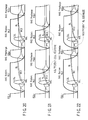
Specifically, when the RAS restore time (tRAS)
becomes shorter because of the power supply voltage,
temperature, or processes as shown in FIG. 21, the cell
will be restored insufficiently. This will make it
impossible to secure a sufficient sense margin for the
next cycle.
When the RAS restore time (tRAS) becomes too long,
for example, the RAS precharge time (tRP) will decrease
as shown in FIG. 22. This will cause the bit lines BL,
bBL to be equalized insufficiently. As a result, cell
data destruction will take place in the sense operation
in the next cycle.
Furthermore, suppose the CR delay decreases in a
long clock cycle (tCK). Then, a RAS precharge
operation is started before the column operation is
completed, which results in an erroneous operation.
This is a serious problem that can occur in the
timer circuit or inverter delay circuit imitating the
operation of the core, although the seriousness of the
problem differs according to the situation.
According to an aspect of the present invention,
there is provided a synchronous semiconductor memory
device comprising: a memory section which includes a
memory cell array having a plurality of memory cells
and which is capable of a read operation of reading
information from the memory cells according to a read
command and a write operation of writing information
into the memory cells according to a write command; a
command sensing circuit which senses whether a first
command inputted in synchronization with an external
clock signal is the read command or the write command;
and a bank timer circuit which, when the command
sensing circuit has sensed either the read command or
the write command, sets the end time of the restore
operation of a row address strobe (RAS) and the start
time of the precharge operation of the RAS according to
the external clock signal.
This summary of the invention does not necessarily
describe all necessary features so that the invention
may also be a sub-combination of these described
features.
The invention can be more fully understood from
the following detailed description when taken in
conjunction with the accompanying drawings, in which:
Hereinafter, referring to the accompanying
drawings, embodiments of the present invention will be
explained.
(First Embodiment)
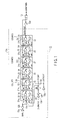
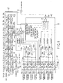
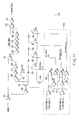
FIG. 1 shows a circuit configuration of a bank
timer (or self-timer circuit) suitable for a
synchronous semiconductor memory device (FCRAM)
according to a first embodiment of the present
invention.
A bank timer 11 comprises inverters 12a to 12g, a
NAND gate 13, a transfer gate 14, and a plurality of
stages (in this case, six stages) of delay sections 21a
to 21f. Each of the delay sections 21a to 21f is
composed of a clocked inverter 22 controlled by signals
CKTRCNT, bCKTRCNT, a clocked inverter 23 controlled by
signals bCKTRCNT, CKTRCNT, and a NAND gate 24.
Specifically, the bank active signal BNKb from the
bank active controller 211 shown in FIG. 15 is supplied
to the input terminal of the inverter 12a. The output
terminal of the inverter 12a is connected to the input
terminal of the inverter 12b. The output terminal of
the inverter 12b is connected to the input terminal of
the inverter 12c and one input terminal of the NAND
gate 13. The output terminal of the inverter 12d is
connected to the other input terminal of the NAND
gate 13.
Furthermore, the output terminal of the inverter
12b is connected to one input terminal of each of the
NAND gate 24 of each of the delay sections 21a to 21f.
The output terminal of each of the clocked inverters
22, 23 is connected to the other input terminal of each
NAND gate 24.
Of the delay sections 21a to 21f, the output
terminal of the NAND gate 24 of each of the delay
sections 21a, 21c, 21e is connected to the input
terminal of the clocked inverter 23 and to the input
terminal of the clocked inverter 23 in each of the
delay sections 21b, 21d, 21f in the next stage. The
output terminal of the NAND gate 24 in each of the
delay sections 21b, 21d is connected to the input
terminal of the clocked inverter 22 and to the input
terminal of the clocked inverter 22 in each of the
delay sections 21c, 21e in the next stage. Of the
delay sections 21a to 21f, the output terminal of the
inverter 12c is connected to the input terminal of the
clocked inverter 22 in the delay section 21a in the
first stage. In the delay section 21f in the final
stage, the output terminal of the NAND gate 24 is
connected to the input terminal of the clocked inverter
22 and to the input terminal of the inverter 12d.
On the other hand, signal CLKINDRVT is supplied to
the input terminal of the inverter 12e. Signal
CLKINDRVT is an internal signal obtained by converting
external clock signal VCLK with an input receiver (not
shown). The output terminal of the inverter 12e is
connected to the input terminal of the inverter 12f.
The output terminal of the inverter 12f is connected to
the input terminal of each of the inverter 12g and
transfer gate 14. The output terminals of the inverter
12g and transfer gate 14 are connected to the control
terminals of the clocked inverters 22, 23,
respectively, in each of the delay sections 21a to 21f.
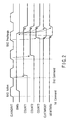
Next, the operation of the bank timer 11 with the
above configuration will be explained by reference to
FIG. 2. When a first command WRA or RDA is received,
signal BNKb goes high. In response to this, COUNT1
goes high after one clock cycle in the clock cycle
counter circuit 11a enclosed by a dotted line in
FIG. 1. After two clock cycles, COUNT2 goes high.
After three clock cycles, COUNT3 goes high. When the
high level of COUNT3 is received, signal CLKTMRDEF goes
low after three clock cycles have elapsed since the
first command. In response to this, signal bBNKTMRb
goes low.
As the end time of RAS restore and the start time
of RAS precharge, three clock cycles from the input of
the first command are counted. On the assumption that
the specification for random cycle (tRC) is five
clocks, three clock cycles are counted as an example of
ideal RAS restore time.
Signal bBNKTMRb, the output of the NAND gate 13,
is inputted to the bank active controller 211 shown in
FIG. 15. Signal bBNKTMRb causes signal BNKb to change
to the low level. This completes the RAS restore
operation and starts the RAS precharge operation.
The low level of signal BNKb resets the bank timer
11. Then, COUNT1, COUNT2, COUNT3 change to the low
level and signals CLKTMRDEF and bBNKTMRb both change to
the high level.
As described above, the bank timer 11 uses
external clock signal VCLK to control the RAS restore
time (tRAS). Specifically, the clock cycle time (tCK)
of signal CLKINDRVT is counted, thereby setting the
timing of the end of the RAS restore operation and the
timing of the start of the RAS precharge operation.
This makes it possible to set a stable RAS restore time
in the FCRAM.
As described above, the self-timer is configured
so as to count clock cycles using external clock signal
VCLK. This makes it possible to suppress variations in
the end time of the RAS restore operation and in the
start time of the RAS precharge operation caused by
variations in the power supply voltage, temperature, or
processes.
Furthermore, the circuit is so configured that the
RAS restore time depends on the clock cycle (tCK).
This makes it possible to secure the RAS restore time
sufficiently, even when the clock cycle is a long
cycle. Therefore, in a series of operations in the
FCRAM, including the RAS restore operation, the
selection of column select lines CSL, and the RAS
precharge operation, it is possible to avoid the
following erroneous operation: the RAS precharge
operation is started before a series of operations in
the column-system circuits is completed, starting with
the selection of column select lines CSL.
(Second Embodiment)
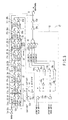
FIG. 3 shows a circuit configuration of a bank
timer suitable for a synchronous semiconductor memory
device (FCRAM) according to a second embodiment of the
present invention. Explanation will be given about a
case where use of a test mode and a fuse blowout
enables the number of clock cycles in the RAS restore
time to be changed.
A bank timer 31 is so configured that a setting
circuit 32 enclosed by a dotted line is added to the
bank timer 11 shown in FIG. 1. In this case, the
setting circuit 32 includes exclusive OR gates 33a,
33b, inverters 34a, 34b, 34c, NOR gates 35a to 35d, an
AND-to-NOR gate 36, clocked inverters 37a to 37d, and
NAND gates 38a, 38b. The setting circuit 32 is
inserted between the inverter 12d and delay section 21f
in the final stage in the bank timer 11.
Test mode signal TMBKTMR<1> is inputted to one
input terminal of the exclusive OR gate 33a. Test mode
signal TMBKTMR<2> is inputted to one input terminal of
the exclusive OR gate 33b. Fuse signals bFSBKTMR<1>,
bFSBKTMR<2> are inputted to the other input terminals
of the exclusive OR gates 33a, 33b, respectively. Test
mode signals TMBKTMR<1>, TMBKTMR<2> are both at the low
level in the initial state. Making an entry of test
mode causes test mode signals TMBKTMR<1>, TMBKTMR<2> to
change to the high level. Test mode signals
TMBKTMR<1>, TMBKTMR<2> can be controlled independently.
Fuse signals bFSBKTMR<1>, bFSBKTMR<2> are both at
the high level in the initial state. A fuse blowout
causes fuse signals bFSBKTMR<1>, bFSBKTMR<2> to change
to the low level. Fuse signals bFSBKTMR<1>,
bFSBKTMR<2> can be controlled independently.
As described above, test mode signal TMBKTMR<1>
and fuse signal bFSBKTMR<1> are inputted to the
exclusive OR gate 33a. Test mode signal TMBKTMR<2> and
fuse signal bFSBKTMR<2> are inputted to the exclusive
OR gate 33b. This enables test mode signals
TMBKTMR<1>, TMBKTMR<2> to change the setting of the RAS
restore time even after the fuse blowout.
The output of the exclusive OR gate 33a is
inputted to each of the NOR gates 35a, 35c and inverter
34a. The output of the inverter 34a is inputted to the
NOR gates 35b, 35d. The output of the exclusive OR
gate 33b is inputted to the NOR gates 35a, 35d and
inverter 34b. The output of the inverter 34b is
inputted to the NOR gates 35b, 35c.
The output CLKTMR<3> of the NOR gate 35a is
supplied to one input terminal of a first AND gate of
the AND-to-NOR gate 36. The output CLKTMRM05 of the
NAND gate 24 in the delay section 21e is supplied to
the other input terminal of the first AND gate. The
output CLKTMR<0> of the NOR gate 35b is supplied to one
input terminal of a second AND gate of the AND-to-NOR
gate 36. The output CLKTMRDEF of the NAND gate 24 in
the delay section 21f in the final stage is supplied to
the other input terminal of the second AND gate. The
output CLKTMR<1> of the NOR gate 35c is supplied to one
input terminal of a third AND gate of the AND-to-NOR
gate 36. The output CLKTMRP05 of the NAND gate 38a is
supplied to the other input terminal of the third AND
gate. The output CLKTMR<2> of the NOR gate 35d is
supplied to one input terminal of a fourth AND gate of
the AND-to-NOR gate 36. The output CLKTMRP10 of the
NAND gate 38b is supplied to the other input terminal
of the fourth AND gate. The output of the NAND-to-NOR
gate 36 is supplied via the inverters 34c, 12d to the
other input terminal of the NAND gate 13.
As described above, in the initial state, test
mode signals TMBKTMR<1>, TMBKTMR<2> are both at the low
level. Fuse signals bFSBKTMR<1>, bFSBKTMR<2> are both
at the high level. In this case, the output CLKTMR<0>
of the NOR gate 35b becomes effective. Specifically,
the output CLKTMRDEF of the NAND gate 24 in the delay
section 21f in the final stage inputted to the AND-to-NOR
gate 36 becomes effective. In this case, the RAS
restore time with the number of clock cycles being 3 is
secured as in the bank timer 11 of the first
embodiment.
Next, a case where test mode signal TMBKTMR<1>
changes to the high level or fuse signal bFSBKTMR<1>
changes to the low level will be explained. In this
case, the output CLKTMR<1> of the NOR gate 35c becomes
effective. Specifically, the output CLKTMRP05 of the
NAND gate 38a inputted to the AND-to-NOR gate 36
becomes effective. Thus, in this case, the RAS restore
time with the number of clock cycles being 3.5 is
secured.
Next, a case where test mode signal TMBKTMR<1>
changes to the high level after fuse signal bFSBKTMR<1>
changes to the low level as a result of a fuse blowout
will be explained. In this case, the output CLKTMR<0>
of the NOR gate 35b becomes effective as in the initial
state. Therefore, the RAS restore time with the number
of clock cycles being 3 is secured.
Next, a case where test mode signal TMBKTMR<2>
changes to the high level or fuse signal bFSBKTMR<2>
changes to the low level will be explained. In this
case, the output CLKTMR<2> of the NOR gate 35d becomes
effective. Specifically, the output CLKTMRP10 of the
NAND gate 38b inputted to the AND-to-NOR gate 36
becomes effective. Thus, in this case, the RAS restore
time with the number of clock cycles being 4 is
secured.
Next, a case where test mode signal TMBKTMR<2>
changes to the high level after fuse signal bFSBKTMR<2>
changes to the low level as a result of a fuse blowout
will be explained. In this case, the output CLKTMR<0>
of the NOR gate 35b becomes effective as in the initial
state. Therefore, the RAS restore time with the number
of clock cycles being 3 is secured.
The following is an explanation of a case where
test mode signal TMBKTMR<1> changes to the high level
or fuse signal bFSBKTMR<1> changes to the low level or
where test mode signal TMBKTMR<2> changes to the high
level or fuse signal bFSBKTMR<2> changes to the low
level. In this case, the output CLKTMR<3> of the NOR
gate 35a becomes effective. Specifically, the output
CLKTMRM05 of the NAND gate 24 in the delay section 21e
inputted to the AND-to-NOR gate 36 becomes effective.
Thus, in this case, the RAS restore time with the
number of clock cycles being 2.5 is secured.
Next, explanation will be given about a case where
test mode signals TMBKTMR<1>, TMBKTMR<2> both change to
the high level after fuse signals bFSBKTMR<1>,
bFSBKTMR<2> both change to the low level as a result of
a fuse blowout. In this case, the output CLKTMR<0> of
the NOR gate 35b becomes effective as in the initial
state. Thus, in this case, the RAS restore time with
the number of clock cycles being 3 is secured.
With the above configuration, the change of the
RAS restore time can be set in units of 0.5 clock
cycles. In the above configuration, test mode signals
TMBKTMR<1>, <2> and fuse signals bFSBKTMR<1>, <2> are
received by the exclusive OR gates 33a, 33b, which
makes it possible to change the setting of the test
mode to the default setting by effecting a fuse blowout
after a check is made in the test mode. Making an
entry of test mode after effecting a fuse blowout
enables the test mode to be returned to the initial
state before the fuse blowout.
In the second embodiment, two kinds of test mode
signals and two kinds of fuse signals have been used.
Use of more test mode signals and more fuse signals
enables a larger number of clock cycles to be set in
units of 0.5 clock cycles.
(Third Embodiment)
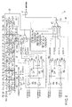
FIG. 4 shows a circuit configuration of a bank
timer suitable for a synchronous semiconductor memory
device (FCRAM) according to a third embodiment of the
present invention. Explanation will be given about a
case where use of a test mode and a fuse blowout
enables fine adjustment of the RAS restore time.
A bank timer 41 is so configured that a fine
adjustment circuit 42 enclosed by a dotted line is
added to the bank timer 31 shown in FIG. 3. In this
case, the fine adjustment circuit 42 includes exclusive
OR gates 43a, 43b, inverters 44a, 44b, 45a to 45l, NOR
gates 46a to 46d, and an AND-to-NOR gate 47. The fine
adjustment circuit 42 is inserted in place of the
inverter 34c in the bank timer 31.
Test mode signal TMBKADJ<1> is inputted to one
input terminal of the exclusive OR gate 43a. Test mode
signal TMBKADJ<2> is inputted to one input terminal of
the exclusive OR gate 43b. Fuse signals bFSBKADJ<1>,
bFSBKADJ<2> are inputted to the other input terminals
of the exclusive OR gates 43a, 43b, respectively.
Test mode signals TMBKADJ<1>, TMBKADJ<2> are both
at the low level in the initial state. Making an entry
of test mode causes test mode signals TMBKADJ<1>,
TMBKADJ<2> to change to the high level. Test mode
signals TMBKADJ<1>, TMBKADJ<2> can be controlled
independently.
Fuse signals bFSBKADJ<1>, bFSBKADJ<2> are both at
the high level in the initial state. A fuse blowout
causes fuse signals bFSBKADJ<1>, bFSBKADJ<2> to change
to the low level. Fuse signals bFSBKADJ<1>,
bFSBKADJ<2> can be controlled independently.
As described above, test mode signal TMBKADJ<1>
and fuse signal bFSBKADJ<1> are inputted to the
exclusive OR gate 43a. Test mode signal TMBKADJ<2> and
fuse signal bFSBKADJ<2> are inputted to the exclusive
OR gate 43b. This enables test mode signals
TMBKADJ<1>, TMBKADJ<2> to change the setting of the RAS
restore time even after the fuse blowout.
The output of the exclusive OR gate 43a is
inputted to each of the NOR gates 46a, 46c and inverter
44a. The output of the inverter 44a is inputted to the
NOR gates 46b, 46d. The output of the exclusive OR
gate 43b is inputted to the NOR gates 46a, 46d and
inverter 44b. The output of the inverter 44b is
inputted to the NOR gates 46b, 46c.
The output DLYADJ<3> of the NOR gate 46a is
supplied to one input terminal of a first AND gate of
the AND-to-NOR gate 47. The output of the AND-to-NOR
gate 36 in the setting circuit 32 is supplied directly
to the other input terminal of the first AND gate. The
output DLYADJ<0> of the NOR gate 46b is supplied to one
input terminal of a second AND gate of the AND-to-NOR
gate 47. The output of the AND-to-NOR gate 36 in the
setting circuit 32 is supplied via the inverters 45a to
45d to the other input terminal of the second AND gate.
The output DLYADJ<1> of the NOR gate 46c is supplied to
one input terminal of a third AND gate of the AND-to-NOR
gate 47. The output of the AND-to-NOR gate 36 in
the setting circuit 32 is supplied via the inverters
45a to 45h to the other input terminal of the third AND
gate. The output DLYADJ<2> of the NOR gate 46d is
supplied to one input terminal of a fourth AND gate of
the AND-to-NOR gate 47. The output of the AND-to-NOR
gate 36 in the setting circuit 32 is supplied via the
inverters 45a to 45l to the other input terminal of the
fourth AND gate. The output of the AND-to-NOR gate 47
is supplied via the inverter 12d to the other input
terminal of the NAND gate 13.
As described above, in the initial state, test
mode signals TMBKADJ<1>, TMBKADJ<2> are both at the low
level. Fuse signals bFSBKADJ<1>, bFSBKADJ<2> are both
at the high level. In this case, the output DLYADJ<0>
of the NOR gate 46b becomes effective. Specifically,
the outputs of the inverters 45a to 45d inputted to the
AND-to-NOR gate 47 become effective. In this case, the
RAS restore time with four stages of delay in the
inverters 45a to 45d is secured.
The following is an explanation of a case where
test mode signal TMBKADJ<1> changes to the high level
or fuse signal bFSBKADJ<1> changes to the low level.
In this case, the output DLYADJ<1> of the NOR gate 46c
becomes effective. Specifically, the outputs of the
inverters 45a to 45h inputted to the AND-to-NOR gate 47
become effective. Thus, in this case, the RAS restore
time with eight stages of delay in the inverters 45a to
45h is secured.
Next, a case where test mode signal TMBKADJ<1>
changes to the high level after fuse signal bFSBKADJ<1>
changes to the low level as a result of a fuse blowout
will be explained. In this case, the output DLYADJ<0>
of the NOR gate 46b becomes effective as in the initial
state. Therefore, in this case, the RAS restore time
with four stages of delay in the inverters 45a to 45d
is secured.
Next, a case where test mode signal TMBKADJ<2>
changes to the high level or fuse signal bFSBKADJ<2>
changes to the low level will be explained. In this
case, the output DLYADJ<2> of the NOR gate 46d becomes
effective. Specifically, the outputs of the inverters
45a to 45l inputted to the AND-to-NOR gate 47 become
effective. Thus, in this case, the RAS restore time
with 12 stages of delay in the inverters 45a to 451 is
secured.
Next, a case where test mode signal TMBKADJ<2>
changes to the high level after fuse signal bFSBKADJ<2>
changes to the low level as a result of a fuse blowout
will be explained. In this case, the output DLYADJ<0>
of the NOR gate 46b becomes effective as in the initial
state. Therefore, the RAS restore time with four
stages of delay in the inverters 45a to 45d is secured.
The following is an explanation of a case where
test mode signal TMBKADJ<1> changes to the high level
or fuse signal bFSBKADJ<1> changes to the low level or
where test mode signal TMBKADJ<2> changes to the high
level or fuse signal bFSBKADJ<2> changes to the low
level. In this case, the output DLYADJ<3> of the NOR
gate 46a becomes effective. Specifically, the output
of the AND-to-NOR gate 36 directly inputted to the AND-to-NOR
gate 47 becomes effective. Thus, in this case,
the RAS restore time without any stage of delay in the
inverters 45a to 451 is secured.
Next, explanation will be given about a case where
test mode signals TMBKADJ<1>, TMBKADJ<2> both change to
the high level after fuse signals bFSBKADJ<1>,
bFSBKADJ<2> both change to the low level as a result of
a fuse blowout. In this case, the output DLYADJ<0> of
the NOR gate 46b becomes effective as in the initial
state. Thus, in this case, the RAS restore time with
four stages of delay in the inverters 45a to 45d is
secured.
As described above, the above configuration
enables fine adjustment of the setting of the RAS
restore time.
In the third embodiment, the RAS restore time fine
adjustment circuit 42 has been composed of inverters.
The present invention is not limited to this. For
instance, similar control can be realized by using CR
delay circuits or other circuits in place of inverters.
In the above configuration, test mode signals
TMBKADJ and fuse signals bFSBKADJ are received by the
exclusive OR gates 43a, 43b, which makes it possible to
change the setting of the test mode to the default
setting by effecting a fuse blowout after a check is
made in the test mode. Making an entry of test mode
after effecting a fuse blowout enables the test mode to
be returned to the initial state before the fuse
blowout.
In the third embodiment, two kinds of test mode
signals and two kinds of fuse signals have been used as
an example. Use of more test mode signals and more
fuse signals makes it possible to make fine adjustment
of more different times.
(Fourth Embodiment)
FIG. 5 shows a circuit configuration of a bank
timer suitable for a synchronous semiconductor memory
device (FCRAM) according to a fourth embodiment of the
present invention. A case where a bank timer that
enables the number of clock cycles in the RAS restore
time and fine adjustment of the RAS restore time to be
set independently by means of CAS latency (CL) will be
explained. The explanation is based on the assumption
that there are two types of CAS latency CL, CL3 and
CL4.
When CAS latency CL changes from CL3 to CL4, the
clock cycle time (tCK) determined in the specification
basically tends to become shorter. For this reason,
when setting is done in such a manner that the count of
the number of clock cycles in the RAS restore time with
CL3 is equal to that with CL4, the RAS restore time
with CL4 is shorter than the with CL3. To overcome
this problem, independent control of the number of
clock cycles in the RAS restore time and fine
adjustment of the RAS restore time is made possible
according to CAS latency. This prevents the RAS
restore time with CL4 from becoming shorter than that
with CL3.
In FIG. 5, a bank timer 51 is such that, for
example, the input section for test mode signals
TMBKTMR<1>, TMBKTMR<2>, TMBKADJ<1>, TMBKADJ<2>, and
fuse signals bFSBKTMR<1>, bFSBKTMR<2>, bFSBKADJ<1>,
bFSBKADJ<2> in the bank timer 41 of FIG. 4 is replaced
with an input circuit 52 enclosed by a dotted line.
That is, a setting section 32' and a fine adjustment
section 42' that include the input circuit 52 are added
to the bank timer shown in FIG. 1. In this case, the
input circuit 52 is composed of exclusive OR gates 53a
to 53h, transfer gates 54a to 54h, and an inverter 55.
Specifically, in the bank timer 51, to enable
independent control using CL3 and CL4, eight input
signals, TMBKTMRCL3<1>, TMBKTMRCL4<1>, TMBKTMRCL3<2>,
TMBKTMRCL4<2>, TMBKADJCL3<1>, TMBKADJCL4<1>,
TMBKADJCL3<2>, TMBKADJCL4<2>, are prepared in place of
test mode signals TMBKTMR<1>, TMBKTMR<2>, TMBKADJ<1>,
TMBKADJ<2> shown in FIG. 4.
Similarly eight input signals, bFSBKTMRCL3<1>,
bFSBKTMRCL4<1>, bFSBKTMRCL3<2>, bFSBKTMRCL4<2>,
bFSBKADJCL3<1>, bFSBKADJCL4<1>, bFSBKADJCL3<2>,
bFSBKADJCL4<2>, are prepared in place of fuse signals
bFSBKTMR<1>, bFSBKTMR<2>, bFSBKADJ<1>, bFSBKADJ<2>.
The test mode signal TMBKTMRCL3<1> is inputted to
one input terminal of the exclusive OR gate 53a. The
fuse signal bFSBKTMRCL3<1> is inputted to the other
input terminal of the exclusive OR gate 53a. The
output of the exclusive OR gate 53a is inputted via the
transfer gate 54a to each of the NOR gates 35a, 35c and
the inverter 34a. The output of the inverter 34a is
inputted to each of the NOR gates 35b, 35d.
The test mode signal TMBKTMRCL4<1> is inputted to
one input terminal of the exclusive OR gate 53b. The
fuse signal bFSBKTMRCL4<1> is inputted to the other
input terminal of the exclusive OR gate 53b. The
output of the exclusive OR gate 53b is inputted via the
transfer gate 54b to each of the NOR gates 35a, 35c and
the inverter 34a.
The test mode signal TMBKTMRCL3<2> is inputted to
one input terminal of the exclusive OR gate 53c. The
fuse signal bFSBKTMRCL3<2> is inputted to the other
input terminal of the exclusive OR gate 53c. The
output of the exclusive OR gate 53c is inputted via the
transfer gate 54c to each of the NOR gates 35a, 35d and
the inverter 34b. The output of the inverter 34b is
inputted to each of the NOR gates 35b, 35c.
The test mode signal TMBKTMRCL4<2> is inputted to
one input terminal of the exclusive OR gate 53d. The
fuse signal bFSBKTMRCL4<2> is inputted to the other
input terminal of the exclusive OR gate 53d. The
output of the exclusive OR gate 53d is inputted via the
transfer gate 54d to each of the NOR gates 35a, 35d and
the inverter 34b.
The test mode signal TMBKADJCL3<1> is inputted to
one input terminal of the exclusive OR gate 53e. The
fuse signal bFSBKADJCL3<1> is inputted to the other
input terminal of the exclusive OR gate 53e. The
output of the exclusive OR gate 53e is inputted via the
transfer gate 54e to each of the NOR gates 46a, 46c and
the inverter 44a. The output of the inverter 44a is
inputted to each of the NOR gates 46b, 46d.
The test mode signal TMBKADJCL4<1> is inputted to
one input terminal of the exclusive OR gate 53f. The
fuse signal bFSBKADJCL4<1> is inputted to the other
input terminal of the exclusive OR gate 53f. The
output of the exclusive OR gate 53f is inputted via the
transfer gate 54f to each of the NOR gates 46a, 46c and
the inverter 44a.
The test mode signal TMBKADJCL3<2> is inputted to
one input terminal of the exclusive OR gate 53g. The
fuse signal bFSBKADJCL3<2> is inputted to the other
input terminal of the exclusive OR gate 53g. The
output of the exclusive OR gate 53g is inputted via the
transfer gate 54g to each of the NOR gates 46a, 46d and
the inverter 44b. The output of the inverter 44b is
inputted to each of the NOR gates 46b, 46c.
The test mode signal TMBKADJCL4<2> is inputted to
one input terminal of the exclusive OR gate 53h. The
fuse signal bFSBKADJCL4<2> is inputted to the other
input terminal of the exclusive OR gate 53h. The
output of the exclusive OR gate 53h is inputted via the
transfer gate 54h to each of the NOR gates 46a, 46d and
the inverter 44b.
When CL3 is used, the transfer gates 54a, 54c,
54e, 54g of the transfer gates 54a to 54h become
effective. When CL4 is used, the transfer gates 54b,
54d, 54f, 54h become effective.
A case where input signal TMBKTMRCL4<1> is made
high in the initial state in the above circuit will be
explained. At this time, with CL3, since test mode
signal TMBKTMRCL4<1> has nothing to do with the setting
of the number of clock cycles, the output CLKTMR<0> of
the NOR gate 35b becomes effective. As a result, the
RAS restore time with the number of clock cycles being
3 is secured.
In contrast, with CL4, because test mode signal
TMBKTMRCL4<1> is at the high level, the output
CLKTMR<1> of the NOR gate 35c becomes effective. As a
result, the RAS restore time with the number of clock
cycles being 3.5 is secured.
Similarly, test mode signal TMBKADJCL4<1> is made
high in the initial state. At this time, with CL3,
test mode signal TMBKADJCL4<1> has nothing to do with
fine adjustment of the RAS restore time, the output
DLYADJ<0> of the NOR gate 46b becomes effective. As a
result, the RAS restore time with four stages of delay
in the inverters 45a to 45d is secured.
In contrast, with CL4, because test mode signal
TMBKADJCL4<1> is at the high level, the output
DLYADJ<1> of the NOR gate 46c becomes effective. As a
result, the RAS restore time with eight stages of delay
in the inverters 45a to 45h is secured.
With the above configuration, the setting of the
RAS restore time can be controlled independently
according to CAS latency CL.
(Fifth Embodiment)
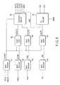
FIG. 6 shows a configuration of a control circuit
for controlling the timing of the change of CAS latency
CL according to a fifth embodiment of the present
invention. A case where the circuit is configured so
as to control the change of CAS latency CL after the
precharge operation of the ROW system is started.
In FIG. 6, external clock signal VCLK and signal
VBCLK are inputted to an input receiver circuit 61,
which then outputs signal CLKINT. The potential VBCS
of the /CS pin is inputted to an input receiver circuit
62, which then outputs signal bCSIN. The potential VFN
of the FN pin is inputted to an input receiver circuit
63, which then outputs signal FNIN. Signal VA is
inputted to an input receiver circuit 64, which then
outputs signal AIN.
Signal CLKINT, the output of the input receiver
circuit 61, and signal bCSIN, the output of the input
receiver circuit 62, are inputted to an input latch
circuit 65, which then outputs signal bCSLTC. Signal
CLKINT, the output of the input receiver circuit 61,
and signal FNIN, the output of the input receiver
circuit 63, are inputted to an input latch circuit 66,
which then outputs signal FNLTC. Signal CLKINT, the
output of the input receiver circuit 61, and signal
AIN, the output of the input receiver circuit 64, are
inputted to an input latch circuit 67, which then
outputs signal AILTC.
Signal CLKINT, the output of the input receiver
circuit 61, signal bCSLTC, the output of the input
latch circuit 65, and signal FNLTC, the output of the
input latch circuit 66, are inputted to a command
decoder circuit 68, which then outputs various
commands, including ACTV, WRITE, READ, REFR, MRS.
Second command MRS, the output of the command decoder
circuit 68, signal AILTC, the output of the input latch
circuit 67, and bank active signal BNKb are inputted
to a CL decoder 69, which then outputs CAS latencies
CL3, CL4.
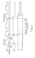
Next, the operation of the control circuit with
the above configuration will be explained by reference
to FIG. 7.
As for the command form in the FCRAM, a mode
register set is recognized by combining a first command
RDA and a second command MRS. In this case, use of
only a first command makes it impossible to distinguish
between a read operation and a mode register set.
Thus, bank active signal BNKb for controlling the ROW
system goes high, thereby starting the active operation
of the ROW system. Then, when use of a second command
MRS enables the mode register set to be recognized
after this operation is completed, the mode, such as
CAS latency (CL) or burst length (BL), is changed.
It is assumed that the bank timer using CL control
receives a second command MRS during the RAS active
operation and immediately switches between CAS latency
CL3 and CAS latency CL4. In this case, there is a
possibility that the clock cycle counter circuit in the
bank timer will malfunction.
To overcome this problem, bank active signal BNKb
is inputted to the CL decoder 69 as shown in FIG. 6.
Then, when bank active signal BNKb goes low, CAS
latency CL3 changes to CAS latency CL4 or vice versa.
As described above, when the precharge operation
of the ROW system is started, or when the operation of
the counter in the bank timer is completed, CAS latency
CL3 changes to CAS latency CL4 or vice versa. This
enables the clock cycle counter circuit to continue the
proper operation even in the bank timer using CL
control.