EP1293823B1 - Commutateur optique comprenant deux réseaux de guides d'ondes optiques non-coplanaires - Google Patents
Commutateur optique comprenant deux réseaux de guides d'ondes optiques non-coplanaires Download PDFInfo
- Publication number
- EP1293823B1 EP1293823B1 EP02018914A EP02018914A EP1293823B1 EP 1293823 B1 EP1293823 B1 EP 1293823B1 EP 02018914 A EP02018914 A EP 02018914A EP 02018914 A EP02018914 A EP 02018914A EP 1293823 B1 EP1293823 B1 EP 1293823B1
- Authority
- EP
- European Patent Office
- Prior art keywords
- waveguide
- waveguides
- optical
- coupling
- switch
- Prior art date
- Legal status (The legal status is an assumption and is not a legal conclusion. Google has not performed a legal analysis and makes no representation as to the accuracy of the status listed.)
- Expired - Lifetime
Links
- 230000003287 optical effect Effects 0.000 title claims description 44
- 238000003491 array Methods 0.000 title 1
- 239000000463 material Substances 0.000 claims description 45
- 230000008878 coupling Effects 0.000 claims description 40
- 238000010168 coupling process Methods 0.000 claims description 40
- 238000005859 coupling reaction Methods 0.000 claims description 40
- 238000005253 cladding Methods 0.000 claims description 12
- 230000008859 change Effects 0.000 claims description 9
- 230000005684 electric field Effects 0.000 claims description 2
- 239000000758 substrate Substances 0.000 description 27
- 239000011159 matrix material Substances 0.000 description 11
- 239000011162 core material Substances 0.000 description 9
- 239000010410 layer Substances 0.000 description 9
- VYPSYNLAJGMNEJ-UHFFFAOYSA-N Silicium dioxide Chemical compound O=[Si]=O VYPSYNLAJGMNEJ-UHFFFAOYSA-N 0.000 description 8
- 239000004973 liquid crystal related substance Substances 0.000 description 8
- 238000000034 method Methods 0.000 description 5
- 239000013307 optical fiber Substances 0.000 description 5
- 230000000694 effects Effects 0.000 description 4
- 239000000377 silicon dioxide Substances 0.000 description 4
- XUIMIQQOPSSXEZ-UHFFFAOYSA-N Silicon Chemical compound [Si] XUIMIQQOPSSXEZ-UHFFFAOYSA-N 0.000 description 3
- 230000008901 benefit Effects 0.000 description 3
- 230000007423 decrease Effects 0.000 description 3
- 239000000835 fiber Substances 0.000 description 3
- 229910052710 silicon Inorganic materials 0.000 description 3
- 239000010703 silicon Substances 0.000 description 3
- 235000012239 silicon dioxide Nutrition 0.000 description 3
- GWEVSGVZZGPLCZ-UHFFFAOYSA-N Titan oxide Chemical compound O=[Ti]=O GWEVSGVZZGPLCZ-UHFFFAOYSA-N 0.000 description 2
- 238000010438 heat treatment Methods 0.000 description 2
- 239000007788 liquid Substances 0.000 description 2
- GQYHUHYESMUTHG-UHFFFAOYSA-N lithium niobate Chemical compound [Li+].[O-][Nb](=O)=O GQYHUHYESMUTHG-UHFFFAOYSA-N 0.000 description 2
- 238000004519 manufacturing process Methods 0.000 description 2
- 239000004065 semiconductor Substances 0.000 description 2
- 229910001218 Gallium arsenide Inorganic materials 0.000 description 1
- 239000004642 Polyimide Substances 0.000 description 1
- 230000005540 biological transmission Effects 0.000 description 1
- 229910052681 coesite Inorganic materials 0.000 description 1
- 238000010276 construction Methods 0.000 description 1
- 239000012792 core layer Substances 0.000 description 1
- 229910052906 cristobalite Inorganic materials 0.000 description 1
- 239000013078 crystal Substances 0.000 description 1
- 230000003247 decreasing effect Effects 0.000 description 1
- 238000009792 diffusion process Methods 0.000 description 1
- 239000011521 glass Substances 0.000 description 1
- 229910052744 lithium Inorganic materials 0.000 description 1
- 238000012986 modification Methods 0.000 description 1
- 230000004048 modification Effects 0.000 description 1
- 229920000620 organic polymer Polymers 0.000 description 1
- 229920001721 polyimide Polymers 0.000 description 1
- 238000012545 processing Methods 0.000 description 1
- 230000004044 response Effects 0.000 description 1
- 229910052682 stishovite Inorganic materials 0.000 description 1
- 238000012546 transfer Methods 0.000 description 1
- 229910052905 tridymite Inorganic materials 0.000 description 1
- 238000001429 visible spectrum Methods 0.000 description 1
Images

Classifications
-
- G—PHYSICS
- G02—OPTICS
- G02F—OPTICAL DEVICES OR ARRANGEMENTS FOR THE CONTROL OF LIGHT BY MODIFICATION OF THE OPTICAL PROPERTIES OF THE MEDIA OF THE ELEMENTS INVOLVED THEREIN; NON-LINEAR OPTICS; FREQUENCY-CHANGING OF LIGHT; OPTICAL LOGIC ELEMENTS; OPTICAL ANALOGUE/DIGITAL CONVERTERS
- G02F1/00—Devices or arrangements for the control of the intensity, colour, phase, polarisation or direction of light arriving from an independent light source, e.g. switching, gating or modulating; Non-linear optics
- G02F1/29—Devices or arrangements for the control of the intensity, colour, phase, polarisation or direction of light arriving from an independent light source, e.g. switching, gating or modulating; Non-linear optics for the control of the position or the direction of light beams, i.e. deflection
- G02F1/31—Digital deflection, i.e. optical switching
- G02F1/313—Digital deflection, i.e. optical switching in an optical waveguide structure
- G02F1/3132—Digital deflection, i.e. optical switching in an optical waveguide structure of directional coupler type
- G02F1/3135—Vertical structure
Definitions
- the present invention relates generally to optical switches and more particularly to waveguide based optical matrix switches.
- Fiber optic networks for transmission of optical signals have come into wide use for telecommunications and data communications in recent years. These fiber optic networks need a rapid, efficient and effective means for switching a channel from one path to another within the network.
- Several switching techniques and structures have been developed in recent years that are satisfactory for many applications for switching a single channel from one path to another. However, these are not entirely satisfactory for functioning as large cross connect switches.
- US-A-5,367,584 discloses a micro-electromechanical photonic switching array comprising a plurality of waveguides which allows to switch a photonic signal between the waveguides.
- portions of the waveguides are mechanically moved in response to either an electrostatic or piezoelectric signal thereby closing an air-gap between the waveguide portions.
- US-A-6,122,416 discloses an optic switch or a switch matrix based on a thermo-optical effect.
- a heater generates a temperature gradient in the vicinity of a crossing point of two waveguides in order to form a difference in the effective refractive index between the cores of the two waveguides.
- the two cores may be arranged in direct contact or with a gap between the two cores.
- the gap material is not influenced by the thermo-optical effects.
- US-A-5,38,1251 discloses an optical switch element for selectively transmitting or shielding light from a first optical wave guide to a second optical wave guide.
- the optical switch element includes a first optical switch portion and a second optical switch portion.
- the first optical switch portion includes a part of said first optical wave guide; a first liquid crystal layer optically connected to said part of said first optical wave guide; a first part of said second optical wave guide optically connected to said first liquid crystal layer; and first voltage applying means for applying voltage to said first liquid crystal layer to change a refractive index of said first liquid crystal layer.
- the second optical switch portion includes a second part of said second optical wave guide; a second liquid crystal layer optically connected to said second part of said second optical wave guide; and second voltage applying means for applying voltage to said second liquid crystal layer to change a refractive index of said second liquid crystal layer.
- said first optical switch portion In a case where light is transmitted from said first optical wave guide to said second optical wave guide, said first optical switch portion is in a transmitting state, and said second optical switch portion is in a shielding state, and in another case where light is shielded from said first optical wave guide to said second optical wave guide, said first optical switch portion is in a shielding state, and said second optical switch portion is in a transmitting state.
- EP 0 813 088 A1 discloses a switching element which defines a transmitting state and a reflecting state for a pair of intersecting waveguides that have a gap at their intersection.
- the switching element exhibits total internal reflection at the gap sidewall from one waveguide to the other when not in the transmitting state.
- index-matching liquid fills the gap, enabling light to continue in the original waveguide direction.
- the switching element may use ink jet techniques or bubble techniques to displace index-matching liquid.
- the present invention provides a cross-point switch in which generally orthogonal waveguides are relatively parallel at their mutual cross point.
- one of two generally orthogonal waveguides can have a 45 degree jog about the cross point, while the other waveguide has a -45 degree jog about the cross point.
- the general orientation of a non-straight waveguide is that of a least-squares-fit straight line for that waveguide.
- a controller controls coupling material between the crossing waveguides to control the optical coupling between the waveguides.
- the waveguides can be formed at opposing faces of respective substrates.
- the elongated waveguides on one plane are generally orthogonal to those on the other plane, except that at the crossing points each waveguide has a 45° jog in such a way that a short portion of both waveguides in a pair of waveguides are parallel at the crossing zone. While the waveguides appear to cross from a plan view perspective, they are spaced from each other. These parallel, spaced segments provide for the optical signal to transfer from the waveguide in one plane to the one it crosses in the other plane. Controllable coupling material is mounted between the parallel waveguide segments in the crossing zone. Switching of optical signals between the waveguides at the crossing zone is accomplished by applying an electronic or a thermal signal to the coupling material between the waveguides.
- crossing angles are contemplated as well as are other ways to form the spaced waveguide planes with coupling material at the crossing zones.
- waveguides that are couplable at a cross point are generally orthogonal to facilitate routing and to minimize unintended coupling away from cross points.
- the present invention provides an increased coupling area.
- the increased coupling area improves power coupling between the waveguides while the coupling material is controlled to promote coupling.
- the present invention decreases the cross point power loss.
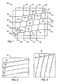
- FIG. 1 of the drawing a diagrammatic top plan view of a waveguide based matrix switch in accordance with an exemplary embodiment of the invention is illustrated and designated generally by reference numeral 10.
- This embodiment comprises main substrate 12 preferably comprised, as will be described, of a first, or lower, substrate 14 and a second, or upper, substrate 16.
- the substrates have a generally rectangular configuration but may have any other suitable shape.
- the illustrated embodiment comprises a generally bi-directional matrix cross connect switch having four optical fiber inputs 18, 20, 22, and 24 on one side and four optical fiber inputs 26, 28, 30, and 32 on a different side.
- the switch body has optical fiber outputs 34, 36, 38, and 40 on a third side and optical fiber outputs 42, 44, 46, and 48 on a side different from the previously identified inputs and outputs.
- Each of optical fiber inputs 18-24 is connected by a respective waveguide 52, 54, 56, 58 directly through to respective optical outputs 34-40 in a common first plane in substrate 14 (see Fig. 2 ).
- optical inputs 26-32 are connected directly through waveguides 60, 62, 64, 66 in a second plane in substrate 16 (see Fig. 3 ) to optical outputs 42-48.
- the two sets of waveguides lie in spaced parallel planes and each has an angled portion at a crossover point where the waveguides in one substate cross at a generally 90° angle to the waveguides in the other substrate.
- the waveguides in lower substrate 14 overlie and cross the waveguides in upper substrate 16 at crossover points where switching is established.
- the upper and lower waveguides are angled and extend along straight parallel sections a short distance at each crossover point. Take, for example, waveguide 60. As shown in Fig. 1 , it crosses over waveguide 52 at cross point 68, where both have straight sections extending parallel to one another.
- Waveguide 62 also extends across waveguide 52 at a cross point 70
- waveguide 64 extends across waveguide 52 at cross point 72
- waveguide 66 extends across waveguide 52 at cross point 74.
- the waveguides are in separate parallel planes, and are generally in a spaced orthogonal relationship to each other from plane to plane, except that they are generally parallel to one another for a short distance in the region of the crossing point.
- the waveguide core is also exposed in the region of the cross point and a layer of coupling material is placed between the two waveguides which can be controlled to act as a switch so that light waves can be made to switch from one waveguide to the other.
- This coupling material undergoes an index of refraction change when subjected to external influence such as thermal or electrical signals.
- the coupling material is selected to be either thermo-optically responsive or electro-optically responsive.
- substrates 14 and 16 are separately shown with waveguides formed therein.
- the waveguides are formed in substrate 14 near its upper surface and in substrate 16 near its bottom surface, so that when the substrates are sandwiched together the substrates are the appropriate distance apart at the crossover points or regions. Optical signals can then be switched or coupled from one waveguide to the other at the crossover points.
- the waveguides may be formed in any one of a number of substrate materials in any suitable manner such as disclosed in U.S. patent 5, 960,131 .
- the substrates are selected to be a suitable material; an example being a semiconductor substrate, such as a silicon wafer or the like. Silicon processing techniques may be used to enable highly accurate fabrication of the waveguides.
- Each waveguide is formed to have a core surrounded by cladding material which is absent between the two waveguides at the crossover point.
- a core layer of material is deposited and etched to form the waveguides. It has been demonstrated that waveguides can be formed in silicon dioxide on silicon substrates.
- the core may be formed of a material that is primarily silicon dioxide, which includes another material such as Ge or TiO 2 .
- the cladding material may be formed of a material that is primarily silicon dioxide but which includes other material such as B 2 O 3 or P 2 O 5 . Because the core material has a refractive index that is different from the refractive index of the cladding layers, optical signals will be guided along the optical waveguide.
- the waveguides are formed in the respective substrates and the substrates are then sandwiched together so that the waveguides extend in spaced, generally parallel planes crossing one another.
- the cladding material is absent from the respective waveguides and a coupling material, such as an electro-optical or thermo-optical material, is deposited between the two cores of the waveguides.
- the waveguides may also be constructed on substrates of other materials such as lithium niobate or a semiconductor such as GaAs by diffusion or crystal growth. Such techniques are disclosed in U.S. patent 4,618,210 .
- FIG. 4 a diagrammatic elevational sectional view of cross point 68 ( Fig. 1 ) is illustrated.
- waveguides 52 and 60 intersect and extend parallel to each other in spaced planes.
- Waveguide 52 is shown formed in substrate 14 as a core with lower cladding 78.
- waveguide 60 Overlying the section of waveguide 52 is waveguide 60 with cladding 78 on one side thereof.
- the cladding is omitted on the sides between the two waveguides.
- This area is filled with a coupling material 80 that is either an electro-optical or a thermo-optical material. The material responds to either an electric field or a thermal input to change the refractive index to switch the light pulses along one or the other of the waveguides over to the other waveguide.
- the coupling material is selected to have an index of refraction equal to that of the cladding until it is activated either by a thermal or electrical input.
- Electro-optical materials that may be used include lithium niobate, lithium tantalite and liquid crystals, among others. There are many different thermo-optical materials that can be used, including S i O 2 , or a large number of polyimides, organic polymers and inorganic glasses, to name a few.
- a pair of elements 82 and 84 are coupled or connected to coupling material 80 and to control circuit 86. Assuming the coupling material is electro-optical, the control circuit applies a voltage across the material to change its refractive index to allow light pulses to cross over from one waveguide to the other. If coupling material 80 is thermo-optical, elements 82, 84 are connected to heating element 88 which changes the temperature of the coupling material and thereby changes the refractive index of the coupling material.
- heating element 86 shown in Fig. 4 does not exist and signals applied to electrodes 82, 84 from control circuit 86 provide the signals to change the index of refraction of the coupling material.
- Figs. 5 and 6 a representation of the operation of switching in the present invention is illustrated.
- Fig. 5 when input light pulses are flowing along waveguide 52 and the index of refraction of the coupling material is the same as the cladding material, the light signals pass by the crossover point and continues along the same waveguide, that is, there is no switching effect.
- Fig. 6 when a control signal is applied to coupling material 80 to change its index of refraction to a value different than that of the cladding, the light pulses migrate from waveguide 52 to waveguide 60 to provide an output signal on fiber output 42 (see Fig. 1 ).
- the illustrated embodiment is shown to be rectangular in configuration. This places the waveguides at a generally ninety-degree angle at the crossover points, with each waveguide having a 45° jog to achieve short parallel segments.
- the switch body may have other configurations such as hexagonal, for example. This would enable the crossover of the waveguides to be at sixty degrees rather than ninety degrees as in the rectangular configuration. Such a construction could have an advantage for some applications. Other angle arrangements could be employed.
- the embodiment as illustrated and described shows the waveguides all having an angled portion at the crossover points. However, it will be appreciated that only one set of the waveguides needs to have an angled portion at the crossover point to extend parallel to the other waveguide, which may remain straight. This can be more easily accomplished where the two sets of waveguides are at less than a ninety-degree angle to one another. Such a configuration could easily be embodied in a hexagonal substrate, for example.
- the upper and lower waveguides could be curved, as could the portions that are parallel and constitute the crossover portion. While the terms “orthogonal” and “parallel" are employed herein, the invention is not so limited. In general, the waveguides in spaced parallel planes are generally more orthogonal than parallel to each other, and the matching crossing segments are generally more parallel than orthogonal to each other.
- the switch assembly could have more than two levels or planes of waveguides and switch between the various levels.
- the terms "light” and “optical” as used herein should not be so construed as to limit the optical signals with which the switch of the invention operates to the visible spectrum.
Landscapes
- Physics & Mathematics (AREA)
- Nonlinear Science (AREA)
- General Physics & Mathematics (AREA)
- Optics & Photonics (AREA)
- Optical Integrated Circuits (AREA)
- Mechanical Light Control Or Optical Switches (AREA)
- Optical Modulation, Optical Deflection, Nonlinear Optics, Optical Demodulation, Optical Logic Elements (AREA)
Claims (5)
- Système de commutation optique comprenant :un premier guide d'ondes (52, 54, 56, 58) s'étendant sur un premier plan, ledit premier guide d'ondes ayant un premier segment de couplage (68, 70, 72, 74) ;un deuxième guide d'ondes (60, 62, 64, 66) s'étendant sur un deuxième plan, ledit deuxième guide d'ondes s'étendant généralement plus orthogonal que parallèle audit premier guide d'ondes, ledit deuxième guide d'ondes ayant un deuxième segment de couplage (68, 70, 72, 74) étendu plus parallèle qu'orthogonal audit premier segment de couplage ;un matériau (80) de couplage disposé entre ledit premier segment de couplage et ledit deuxième segment de couplage, ledit matériau (80) de couplage ayant un indice de réfraction qui peut être commandé sélectivement pour commander le couplage de lumière entre ledit premier guide d'ondes et ledit deuxième guide d'ondes ;
caractérisé en ce quelesdits guides d'ondes sont munis d'une gaine (78) excepté dans la zone dudit deuxième segment (68, 70, 72, 74) de couplage, etledit matériau (80) de couplage a un indice de réfraction sensiblement égal à celui de ladite gaine (78) jusqu'à son activation. - Système selon la revendication 1, dans lequel ledit matériau (80) de couplage réagit à un champ électrique pour modifier son indice de réfraction.
- Système selon la revendication 1, dans lequel ledit matériau (80) de couplage réagit à la chaleur pour modifier son indice de réfraction.
- Système selon l'une des revendications 1 à 3, et comprenant en outre :un moyen (86) de modifier sélectivement l'indice de réfraction dudit matériau de couplage.
- Système selon la revendication 4, dans lequel ledit moyen (86) comprend un dispositif de commande permettant de modifier l'indice de réfraction dudit matériau de couplage.
Applications Claiming Priority (2)
| Application Number | Priority Date | Filing Date | Title |
|---|---|---|---|
| US956413 | 2001-09-18 | ||
| US09/956,413 US6738541B2 (en) | 2001-09-18 | 2001-09-18 | Optical switch comprising two non-coplanar arrays of optical waveguides |
Publications (3)
| Publication Number | Publication Date |
|---|---|
| EP1293823A2 EP1293823A2 (fr) | 2003-03-19 |
| EP1293823A3 EP1293823A3 (fr) | 2003-10-08 |
| EP1293823B1 true EP1293823B1 (fr) | 2009-09-30 |
Family
ID=25498219
Family Applications (1)
| Application Number | Title | Priority Date | Filing Date |
|---|---|---|---|
| EP02018914A Expired - Lifetime EP1293823B1 (fr) | 2001-09-18 | 2002-08-23 | Commutateur optique comprenant deux réseaux de guides d'ondes optiques non-coplanaires |
Country Status (4)
| Country | Link |
|---|---|
| US (1) | US6738541B2 (fr) |
| EP (1) | EP1293823B1 (fr) |
| JP (1) | JP4330318B2 (fr) |
| DE (1) | DE60233849D1 (fr) |
Families Citing this family (9)
| Publication number | Priority date | Publication date | Assignee | Title |
|---|---|---|---|---|
| IL140318A0 (en) * | 2000-12-14 | 2002-02-10 | Planop Planar Optics Ltd | Compact dynamic crossbar switch by means of planar optics |
| JP2002258081A (ja) * | 2001-02-28 | 2002-09-11 | Fujitsu Ltd | 光配線基板、光配線基板の製造方法及び多層光配線 |
| JP4734053B2 (ja) * | 2005-07-14 | 2011-07-27 | 富士通株式会社 | 光導波路部品の実装ずれ補償方法 |
| RU2345392C1 (ru) * | 2007-08-13 | 2009-01-27 | Закрытое Акционерное Общество "Научно-Производственное Предприятие "Мифотекс" | Интегральный многоканальный волоконно-оптический коммутатор |
| US8909007B2 (en) * | 2010-10-29 | 2014-12-09 | Hewlett-Packard Development Company, L.P. | Circuit switchable optical device |
| US20180045893A1 (en) * | 2014-12-19 | 2018-02-15 | CommScope Connectivity Belgium BVBA | Integrated optical switching and splitting for optical networks |
| CN110456455B (zh) * | 2018-07-20 | 2020-08-04 | 西安电子科技大学 | 基于等离子体-光交换模块的片上光交换结构 |
| KR20200092123A (ko) * | 2019-01-24 | 2020-08-03 | 한국전자통신연구원 | 3차원 광스위치 |
| EP4062213A4 (fr) * | 2019-11-19 | 2023-11-22 | HRL Laboratories LLC | Commutateur de guide d'ondes optique 3d à commande électrique doté de matériaux à changement de phase |
Family Cites Families (13)
| Publication number | Priority date | Publication date | Assignee | Title |
|---|---|---|---|---|
| US3849740A (en) * | 1973-05-01 | 1974-11-19 | Westinghouse Electric Corp | Integrated optical and/or gate |
| US4618210A (en) | 1982-06-09 | 1986-10-21 | Nec Corporation | Optical switch of switched directional coupler type |
| US5157748A (en) | 1990-09-28 | 1992-10-20 | Siemens Aktiengesellschaft | Controllable integrated optical directional coupler |
| US5381251A (en) | 1992-04-07 | 1995-01-10 | Sharp Kabushiki Kaisha | Optical switch element and a liquid crystal light directional coupler used in the optical switch element |
| US5581108A (en) * | 1993-09-09 | 1996-12-03 | Electronics & Telecommunications Research Institute | Optical Switching device |
| US5367584A (en) * | 1993-10-27 | 1994-11-22 | General Electric Company | Integrated microelectromechanical polymeric photonic switching arrays |
| US5699462A (en) | 1996-06-14 | 1997-12-16 | Hewlett-Packard Company | Total internal reflection optical switches employing thermal activation |
| US6122416A (en) * | 1997-09-26 | 2000-09-19 | Nippon Telegraph And Telephone Corporation | Stacked thermo-optic switch, switch matrix and add-drop multiplexer having the stacked thermo-optic switch |
| US6055344A (en) * | 1998-02-18 | 2000-04-25 | Hewlett-Packard Company | Fabrication of a total internal reflection optical switch with vertical fluid fill-holes |
| DE19849862C1 (de) * | 1998-10-29 | 2000-04-06 | Alcatel Sa | Thermooptischer Schalter |
| US6385376B1 (en) * | 1998-10-30 | 2002-05-07 | The Regents Of The University Of California | Fused vertical coupler for switches, filters and other electro-optic devices |
| US6327397B1 (en) * | 2000-02-22 | 2001-12-04 | Agilent Technologies, Inc. | System and method for providing temperature control for a thermally activated optical switch using constant total power |
| US6459828B1 (en) * | 2000-04-29 | 2002-10-01 | Agilent Technologies, Inc. | Rearrangeable optical add/drop multiplexor switch with low loss |
-
2001
- 2001-09-18 US US09/956,413 patent/US6738541B2/en not_active Expired - Fee Related
-
2002
- 2002-08-23 EP EP02018914A patent/EP1293823B1/fr not_active Expired - Lifetime
- 2002-08-23 DE DE60233849T patent/DE60233849D1/de not_active Expired - Lifetime
- 2002-09-12 JP JP2002266168A patent/JP4330318B2/ja not_active Expired - Fee Related
Also Published As
| Publication number | Publication date |
|---|---|
| JP4330318B2 (ja) | 2009-09-16 |
| US6738541B2 (en) | 2004-05-18 |
| EP1293823A3 (fr) | 2003-10-08 |
| JP2003140207A (ja) | 2003-05-14 |
| US20030053741A1 (en) | 2003-03-20 |
| DE60233849D1 (de) | 2009-11-12 |
| EP1293823A2 (fr) | 2003-03-19 |
Similar Documents
| Publication | Publication Date | Title |
|---|---|---|
| US6453086B1 (en) | Piezoelectric optical switch device | |
| KR102427251B1 (ko) | 집적 광학 기반의 광 응력 위상 변조기 | |
| EP2513715B1 (fr) | Dispositif et procede pour la guidage des ondes optiques | |
| US6411752B1 (en) | Vertically coupled optical resonator devices over a cross-grid waveguide architecture | |
| US6687425B2 (en) | Waveguides and devices incorporating optically functional cladding regions | |
| US20010046363A1 (en) | Variable optical attenuators and optical shutters using a coupling layer in proximity to an optical waveguide (II) | |
| US20020021878A1 (en) | Active photonic crystal waveguide device and method | |
| WO1989006813A1 (fr) | Jonction de guide d'ondes optique | |
| GB2297388A (en) | Integrated optical switching or modulating device using magnetostrictively, electrostrictively or photostrictively induced stress | |
| KR101063957B1 (ko) | 폴리머 삽입형 실리카 광도파로를 이용하는 전반사형 광 스위치 및 그의 제조 방법 | |
| KR20030089492A (ko) | 도파로형 액정 광 스위치 | |
| EP1293823B1 (fr) | Commutateur optique comprenant deux réseaux de guides d'ondes optiques non-coplanaires | |
| US4172630A (en) | Multimode electrooptic waveguide switch | |
| US20020034352A1 (en) | Optical switch device having an integrated polymer switching element | |
| CA2403689A1 (fr) | Dephaseur optique de guides d'ondes | |
| US6968105B2 (en) | Waveguide-type optical device and optical switch | |
| JPH11237652A (ja) | 導波路型光スイッチ | |
| US6959124B2 (en) | Liquid crystal-based electro-optical device forming, in particular, a switch | |
| JP2004325536A (ja) | 非線形光デバイス | |
| EP1382984A1 (fr) | Commutateur en optique planaire et matrice de commutateurs | |
| KR20020064908A (ko) | 통합 평면 광학 도파관 및 셔터 | |
| WO2001067166A1 (fr) | Attenuateurs optiques variables | |
| KR100370278B1 (ko) | 광 경로 제어용 투 바이 투 광스위치 | |
| Goel et al. | Design considerations for crossing channel switches | |
| CA2363766A1 (fr) | Commutateur optique piezo-electrique |
Legal Events
| Date | Code | Title | Description |
|---|---|---|---|
| PUAI | Public reference made under article 153(3) epc to a published international application that has entered the european phase |
Free format text: ORIGINAL CODE: 0009012 |
|
| AK | Designated contracting states |
Kind code of ref document: A2 Designated state(s): AT BE BG CH CY CZ DE DK EE ES FI FR GB GR IE IT LI LU MC NL PT SE SK TR Designated state(s): AT BE BG CH CY CZ DE DK EE ES FI FR GB GR IE IT LI LU MC NL PT SE SK TR |
|
| AX | Request for extension of the european patent |
Extension state: AL LT LV MK RO SI |
|
| PUAL | Search report despatched |
Free format text: ORIGINAL CODE: 0009013 |
|
| AK | Designated contracting states |
Kind code of ref document: A3 Designated state(s): AT BE BG CH CY CZ DE DK EE ES FI FR GB GR IE IT LI LU MC NL PT SE SK TR |
|
| AX | Request for extension of the european patent |
Extension state: AL LT LV MK RO SI |
|
| 17P | Request for examination filed |
Effective date: 20040309 |
|
| AKX | Designation fees paid |
Designated state(s): DE GB |
|
| RAP1 | Party data changed (applicant data changed or rights of an application transferred) |
Owner name: AVAGO TECHNOLOGIES FIBER IP (SINGAPORE) PTE. LTD. |
|
| 17Q | First examination report despatched |
Effective date: 20050818 |
|
| GRAP | Despatch of communication of intention to grant a patent |
Free format text: ORIGINAL CODE: EPIDOSNIGR1 |
|
| GRAS | Grant fee paid |
Free format text: ORIGINAL CODE: EPIDOSNIGR3 |
|
| GRAA | (expected) grant |
Free format text: ORIGINAL CODE: 0009210 |
|
| AK | Designated contracting states |
Kind code of ref document: B1 Designated state(s): DE GB |
|
| REG | Reference to a national code |
Ref country code: GB Ref legal event code: FG4D |
|
| REF | Corresponds to: |
Ref document number: 60233849 Country of ref document: DE Date of ref document: 20091112 Kind code of ref document: P |
|
| PLBE | No opposition filed within time limit |
Free format text: ORIGINAL CODE: 0009261 |
|
| STAA | Information on the status of an ep patent application or granted ep patent |
Free format text: STATUS: NO OPPOSITION FILED WITHIN TIME LIMIT |
|
| 26N | No opposition filed |
Effective date: 20100701 |
|
| PGFP | Annual fee paid to national office [announced via postgrant information from national office to epo] |
Ref country code: GB Payment date: 20100818 Year of fee payment: 9 |
|
| REG | Reference to a national code |
Ref country code: DE Ref legal event code: R119 Ref document number: 60233849 Country of ref document: DE Effective date: 20110301 |
|
| PG25 | Lapsed in a contracting state [announced via postgrant information from national office to epo] |
Ref country code: DE Free format text: LAPSE BECAUSE OF NON-PAYMENT OF DUE FEES Effective date: 20110301 |
|
| GBPC | Gb: european patent ceased through non-payment of renewal fee |
Effective date: 20110823 |
|
| PG25 | Lapsed in a contracting state [announced via postgrant information from national office to epo] |
Ref country code: GB Free format text: LAPSE BECAUSE OF NON-PAYMENT OF DUE FEES Effective date: 20110823 |