EP1292161A1 - Dispositif d'alimentation à découpage adapté pour les faibles consommations de courant, et téléphone cellulaire doté d'un tel dispositif - Google Patents
Dispositif d'alimentation à découpage adapté pour les faibles consommations de courant, et téléphone cellulaire doté d'un tel dispositif Download PDFInfo
- Publication number
- EP1292161A1 EP1292161A1 EP02368097A EP02368097A EP1292161A1 EP 1292161 A1 EP1292161 A1 EP 1292161A1 EP 02368097 A EP02368097 A EP 02368097A EP 02368097 A EP02368097 A EP 02368097A EP 1292161 A1 EP1292161 A1 EP 1292161A1
- Authority
- EP
- European Patent Office
- Prior art keywords
- output
- input
- flip
- voltage
- ramp
- Prior art date
- Legal status (The legal status is an assumption and is not a legal conclusion. Google has not performed a legal analysis and makes no representation as to the accuracy of the status listed.)
- Granted
Links
- 230000001413 cellular effect Effects 0.000 title claims description 3
- 239000003990 capacitor Substances 0.000 claims description 14
- 230000001105 regulatory effect Effects 0.000 claims description 14
- 230000001276 controlling effect Effects 0.000 claims description 8
- 230000001934 delay Effects 0.000 claims description 6
- 230000008033 biological extinction Effects 0.000 claims description 5
- 238000001514 detection method Methods 0.000 claims 2
- 238000007599 discharging Methods 0.000 claims 1
- 238000005516 engineering process Methods 0.000 description 5
- 238000010586 diagram Methods 0.000 description 4
- 230000008901 benefit Effects 0.000 description 2
- 125000004122 cyclic group Chemical group 0.000 description 2
- 230000000694 effects Effects 0.000 description 2
- 238000000034 method Methods 0.000 description 2
- 239000004065 semiconductor Substances 0.000 description 2
- HBBGRARXTFLTSG-UHFFFAOYSA-N Lithium ion Chemical compound [Li+] HBBGRARXTFLTSG-UHFFFAOYSA-N 0.000 description 1
- 230000005540 biological transmission Effects 0.000 description 1
- 239000013256 coordination polymer Substances 0.000 description 1
- 230000002089 crippling effect Effects 0.000 description 1
- 230000003247 decreasing effect Effects 0.000 description 1
- 230000003111 delayed effect Effects 0.000 description 1
- 238000005265 energy consumption Methods 0.000 description 1
- RVRCFVVLDHTFFA-UHFFFAOYSA-N heptasodium;tungsten;nonatriacontahydrate Chemical compound O.O.O.O.O.O.O.O.O.O.O.O.O.O.O.O.O.O.O.O.O.O.O.O.O.O.O.O.O.O.O.O.O.O.O.O.O.O.O.[Na+].[Na+].[Na+].[Na+].[Na+].[Na+].[Na+].[W].[W].[W].[W].[W].[W].[W].[W].[W].[W].[W] RVRCFVVLDHTFFA-UHFFFAOYSA-N 0.000 description 1
- 229910052744 lithium Inorganic materials 0.000 description 1
- 229910001416 lithium ion Inorganic materials 0.000 description 1
- 230000000630 rising effect Effects 0.000 description 1
- 238000005070 sampling Methods 0.000 description 1
- 238000004088 simulation Methods 0.000 description 1
- 230000002618 waking effect Effects 0.000 description 1
Images




Classifications
-
- H—ELECTRICITY
- H02—GENERATION; CONVERSION OR DISTRIBUTION OF ELECTRIC POWER
- H02M—APPARATUS FOR CONVERSION BETWEEN AC AND AC, BETWEEN AC AND DC, OR BETWEEN DC AND DC, AND FOR USE WITH MAINS OR SIMILAR POWER SUPPLY SYSTEMS; CONVERSION OF DC OR AC INPUT POWER INTO SURGE OUTPUT POWER; CONTROL OR REGULATION THEREOF
- H02M3/00—Conversion of DC power input into DC power output
- H02M3/02—Conversion of DC power input into DC power output without intermediate conversion into AC
- H02M3/04—Conversion of DC power input into DC power output without intermediate conversion into AC by static converters
- H02M3/10—Conversion of DC power input into DC power output without intermediate conversion into AC by static converters using discharge tubes with control electrode or semiconductor devices with control electrode
- H02M3/145—Conversion of DC power input into DC power output without intermediate conversion into AC by static converters using discharge tubes with control electrode or semiconductor devices with control electrode using devices of a triode or transistor type requiring continuous application of a control signal
- H02M3/155—Conversion of DC power input into DC power output without intermediate conversion into AC by static converters using discharge tubes with control electrode or semiconductor devices with control electrode using devices of a triode or transistor type requiring continuous application of a control signal using semiconductor devices only
- H02M3/156—Conversion of DC power input into DC power output without intermediate conversion into AC by static converters using discharge tubes with control electrode or semiconductor devices with control electrode using devices of a triode or transistor type requiring continuous application of a control signal using semiconductor devices only with automatic control of output voltage or current, e.g. switching regulators
Definitions
- the present invention relates to feeding circuits, and in particular a switching power supply device adapted for low consumption of current.
- Portable electronic circuits are developing and becoming more widespread. They are powered by batteries - whose design is also constantly development - which provide them with the energy they need to operate.
- the field of mobile telephony particularly illustrates this development of mobile electronics powered by electric battery.
- cell phones conform to the Global standard Mobile Service, require a high inrush current when in use operation. On the contrary, during the waking period, they settle for a particularly low consumption, which is being constantly developing engineers of these devices.
- FIG. 1 shows an illustration of a conventional architecture of a switching power supply device for a cell phone for example.
- a power circuit composed of a PMOS transistor 101, associated with a freewheeling diode 104, and the assembly supplies current to a load (not shown) via an LC quadrupole composed of an inductor or self 102 and a capacitor 103.
- the power circuit is controlled by a control circuit based on a comparator 109 and a ramp generator - composed of a transistor 114 and a capacitor 115 charged by a bias current.
- An amplifier circuit consisting of an Operational Amplifier (AO) 106 associated with a feedback circuit comprising a resistor 107 and a capacitor 108 connected in parallel, amplifies the error between the output voltage to be regulated V out , and a reference voltage V ref .
- the output of this amplifier is sent to one of the two inputs of the comparator receiving at its second input the ramp voltage.
- the comparator periodically at the frequency of a clock signal, the comparator generates a cyclic signal whose duty cycle depends on the difference between the voltage V out and the reference voltage V ref .
- the opening duty cycle of the power transistor 101 is thus regulated so as to bring the output voltage V out closer to the desired value V ref .
- the MOS transistor 101 which supplies the load current is turned on and the ramp signal is then started.
- the ramp voltage reaches the value of the error voltage at the output of the error amplifier, the latter switches and comes to block the control of the power MOS. If we imagine that the voltage V out falls below the setpoint value V ref , we see that the error signal tends to increase, which has the effect of increasing the duty cycle - and in particular the factor T on corresponding to the conduction of the power transistor 101.
- the voltage V ref makes it possible to adjust the value of the voltage V out which is desired, and a regulating effect of this output voltage is observed thanks to the control of the opening time - T on - of the transistor d 'food.
- T on To reduce the value of T on , we traditionally opt for a faster comparator to reduce the intrinsic switching time, but this is done at the cost of a higher power consumption. In doing so, the value of T on is then reduced in absolute terms. Another known way avoids the loss of efficiency resulting from the use of a faster comparator. It consists in acting on the relative value of the duty cycle T on / T by reducing the operating frequency of the switched-mode power supply so as to enter an operating regime known as the Anglo-Saxon pulse-skipping system . By reducing the operating frequency from 1Mhz to 50 Khz for example, we can reduce the duty cycle in a ratio of one twentieth without being forced to opt for a faster comparator.
- the present invention aims to propose a feed structure to cutting with a high yield, and which allows operation to constant frequency even when one is in low power consumption.
- Another object of the present invention is to propose a device switching power supply which is particularly suitable for mobile phone technology of the new generation.
- the circuit is characterized by the existence of a delay circuit to the setting conduction of the power transistor so as to desynchronize the start of the ramp and said conduction of the supply transistor.
- the output of the comparator is connected to a flip-flop - for example type D - and said comparator is disabled once the comparison performed to further reduce energy consumption.
- the delay circuit has a first and second latch having an input D receiving a potential of reference.
- a clock signal comes periodically to control the sampling both latches and their zeroing is controlled by the output of the comparator.
- the output of the first flip-flop is transmitted via a delay line to a first input of an AND gate, which has a second input connected to the output of the second flip-flop D.
- the AND gate provides a control signal for the power transistor. Due to the existence of the delay line, it is ensured and a delayed switching of the output of the AND gate relative to the instant of switching of the second flip-flop, which is used to control the setting zero of the ramp generation circuit.
- the conduction of the power transistor is ensured with a delay while its extinction is immediate when switching the second rocker.
- Figure 1 illustrates the block diagram of a switching power supply based on a comparator and a ramp generation circuit.
- FIG. 2 represents a switching power supply modified so as to allow the use of the lowest values of the duty cycle.
- FIG. 3 illustrates a preferred embodiment of the power supply cutting, comprising two D flip-flops to ensure desynchronization between the control of the ramp generation circuit and the turning on of the power transistor.
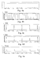
- FIGS. 4a to 4e illustrate the operation of the circuit in the absence of any desynchronization.
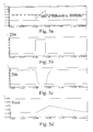
- FIGS. 5a to 5d illustrate the detail of the chronograms of FIGS. 4th.
- FIGS. 6a to 6e illustrate the operation of the circuit when the implementation conduction of the power transistor is out of sync with the starting the ramp generation.
- FIGS. 7a to 7d illustrate the detail of the chronograms of FIGS. 6th.
- the circuit is particularly suitable for designing a power supply circuit for a new generation cell phone.
- a modern cell phone usually has a digital signal processing processor (DSP) that is a large power consumer in active mode and is associated with a microcontroller for keyboard, screen, user interface management. etc ...., which requires a much lower power supply. It is thus possible, in a standby mode, to operate the phone with a very low power supply while in an active operating mode - when the user is using his phone - the DSP functionalities are fully implemented. in the device, thus substantially increasing the current consumed by the phone.
- the switching power supply circuit because it allows operation even for very low values of the duty cycle, is therefore particularly suitable for powering cell phones that have these two very different modes of operation. It is however clear that the skilled person can adapt the teaching of the invention to any other mobile electronic device.
- FIG. 2 thus shows a PMOS transistor 101 whose source is connected to an unregulated voltage source, which is generally provided by a battery of the Ion-Lithium type, for example.
- this type of battery has nominal voltages equal to several volts and it is necessary to reduce the output voltage to prescribed values that are compatible with the semiconductor product technology used, for example between 0.9 or 1.2. Volts.
- the drain of the PMOS transistor is connected to ground via a freewheel diode 105 and also connected to a first electrode of a choke 102 connected in series with a capacitor 103.
- the regulated output voltage V out is accessible across the capacitors. 103 and can serve as a supply voltage for a given load (not shown).
- This control system comprises an Operational Amplifier (AO) 106 whose positive input receives a reference voltage filtered by a capacitor 113.
- the AO 106 is mounted in linear amplifier with a feedback loop, which is composed of a resistor 107 and a capacitor 108 which are connected in parallel and the assembly makes it possible to generate an error signal representative of the difference between the regulated voltage V out and the reference voltage V ref .
- the error signal at the output of the AO 106 is transmitted to a positive input of a second AO 109, mounted in a comparator circuit, and whose negative input receives a ramp voltage generated by a ramp generation circuit based on on a transistor 114 which is associated with a capacitor 115.
- the output of the AO 109 is transmitted via a flip-flop 110, for example of the D flip-flop type, and an inverter 116 to a gate input of the PMOS power transistor 101, via a delay element 100.
- the delay element 100 is designed to introduce a predetermined delay on the falling edges of the gate signal of the PMOS transistor 101, that is to say a delay in the conduction of the latter. In order for the system to operate satisfactorily by compensating for the delays inherent in the comparator 109, or even the flip-flop 110, it must be observed that the delay element 100 must introduce a delay in switching on but not in tripping. It will be seen below that this element can be made in a simple manner when the preferred embodiment of FIG. 3 is described. By introducing a delay in turning on power transistor 101, it is possible to to introduce a local desynchronization by starting the generation of the ramp before turning on the power transistor 101 and therefore we can compensate for all switching times in the chain.
- capacitor pairing techniques and current mirrors which are well known to those skilled in the art, which will allow to precisely adjust the delay of the element 100 so as to make operate the switching power supply in a wide range of output currents, and especially for the weakest values.
- FIG. 3 shows a preferred embodiment of the circuit of desynchronization comprising a first flip-flop 202 and a second flip-flop 203.
- the two flip-flops 202 and 203 each have an input D and an input SD that are connected to the positive supply voltage. They receive at a CP input a clock signal CLK 205 for timing the generation of the ramp and representative timing diagrams are shown in Figure 6b.
- Flip-flops 202 and 203 are reset by means of a signal presented to their CD input, which is connected to the output of the comparator 109.
- the first flip-flop 202 has an output Q which is connected to a input of a delay element 297 whose output is connected to a first entrance of an ET 201 door.
- the second flip-flop 203 has an output Q which is connected to a second entrance of the gate ET 201, but also serves circuit 204 of control of the ramp generator comprising transistor 114, the capacitor 115 and a current source 117.
- this time we connected the output of the circuit ramp generation at the positive input of the comparator circuit 109, unlike the representation of Figure 2.
- the comparator output is then connected directly to two CD inputs flip-flops 202 and 203 and thus serves as reset for these two flip-flops.
- the AND gate 201 provides an output voltage 206 for controlling the conduction of the power MOS transistor 101 which is represented on the Figure 1. It may be possible to add, where necessary, a circuit of buffer type adequate (not shown).
- the operation of the desynchronization circuit is as follows. We assume the power transistor in a state of non-conduction. On the rising front of the clock signal CLK, present on the electrode 205, the output Q of the two flip-flops goes to a high state. This high state is transmitted immediately to the second input of the AND gate and also command via circuit 204 the start of the ramp of the ramp generator. However, it is only when the high state is transmitted by the delay element 207 to the first input of the AND gate 201 that the latter sees its output switch, thus bringing into conduction the MOS power transistor.
- Figures 4a-e and 5a-d illustrate simulation timing diagrams of different voltages existing in the supply circuit when maintaining the synchronization between the zeroing of the ramp generator circuit and the implementation of conduction of the power transistor.
- Figure 4a illustrates the charging current curve.
- Figure 4b illustrates the clock signal 205.
- FIG. 4c shows the output signal Q of the second flip-flop, which control the zero of the ramp generator circuit.
- FIG. 4d illustrates the voltage 206 at the output of the AND gate 201, which serves to controlling the turning on of the power transistor 101.
- Figure 4 e shows the voltage V out across the load.
- FIG. 5a particularly illustrates in detail the signal at the input of the comparator 109.
- FIG. 5b particularly illustrates in detail the output signal Q 204 of FIG. second flip-flop, which controls the zeroing of the generator circuit of ramp.
- FIG. 5c particularly illustrates in detail the voltage 206 at the output of the ET gate 201, which serves to control the conduction of the transistor of power 101.
- Figure 5d shows the detail of the output voltage V out across the load.
- Figures 6a-e and 7a-d illustrate representative chronograms of the same voltage when the desynchronization between the start of the ramp and the conduction of the power transistor 101.
- Figure 6a illustrates the charging current curve
- Figure 6b illustrates the clock signal 205.
- FIG. 6c shows the output signal Q of the second flip-flop 203, which just control the zeroing of the ramp generator circuit.
- FIG. 6d illustrates the voltage 206 at the output of the AND gate 201, which serves to controlling the turning on of the power transistor 101.
- Figure 6e shows the voltage V out across the load.
- Figure 7a particularly illustrates in detail the signal at the input of comparator 109.
- FIG. 7b particularly illustrates in detail the signal Q 204 output from the second flip-flop, which controls the zeroing of the generator circuit of ramp.
- FIG. 7c particularly illustrates in detail the voltage 206 at the output of the ET gate 201, which serves to control the conduction of the transistor of power 101.
- Figure 7 d shows the detail of the output voltage V out across the load.
- the desynchronization can substantially reduce the time required for conduction of the power transistor, without having to resort to a comparator 109 faster.
Landscapes
- Engineering & Computer Science (AREA)
- Power Engineering (AREA)
- Dc-Dc Converters (AREA)
Abstract
Description
Claims (9)
- Dispositif d'alimentation à découpage composé d'un transistor de puissance mis cycliquement en conduction suivant un rapport cyclique Ton/T et fournissant un courant et une tension régulée (Vout) à une charge via un filtre LC, lequel comportantun circuit de génération d'une rampe (114, 115) commandé par un signal d'horloge et fournissant cycliquement une tension de rampe ;un circuit amplificateur d'erreur (106) pour générer une tension d'erreur représentative de l'écart entre une tension de référence et ladite tension de sortie régulée ;un comparateur (109) comparant la tension de rampe générée par ledit circuit de génération de rampe (114, 115) avec ladite tension d'erreur et fournissant un signal de sortie destiné à commander ledit circuit de puissance.le dispositif étant caractérisé en ce que un élément de retard (100) vient retarder la mise en conduction dudit transistor de puissance de manière à désynchroniser le démarrage de la rampe et ladite mise en conduction.
- Dispositif d'alimentation à découpage selon la revendication 1 caractérisé en ce que ledit comparateur est connecté à une entrée d'une bascule et est ensuite désactivé dès la comparaison effectuée.
- Dispositif d'alimentation à découpage selon la revendication 1 caractérisé en ce qu'il comporte :un premier Amplificateur Opérationnel (A.O.) 106 dont l'entrée positive reçoit une tension de référence et monté en amplificateur linéaire pour générer un signal d'erreur représentatif de l'écart entre la tension régulée Vout et la tension de référence Vref, ledit premier AO (106) étant monté avec une boucle de contre-réaction composée d'une résistance (107) et d'un condensateur (108) montés en parallèle,un circuit de génération de rampe (114, 115) ayant une entrée de mise à zéro pour générer une tension de rampe dès la détection d'un signal de mise à zéro ;un second Amplificateur Opérationnel (109) monté en comparateur, et recevant à une première entrée ledit signal d'erreur générée par la sortie dudit premier Amplificateur Opérationnel (106) et recevant à une seconde entrée une tension de sortie générée par ledit circuit de génération de rampe ;une bascule D (110) recevant en entrée la tension de sortie dudit second amplificateur Opérationnel (109),un inverseur (116) dont l'entrée est connecté à la sortie de ladite bascule D , ledit inverseur (116) ayant une sortie connectée à l'entrée de mise à zéro dudit circuit de génération de rampe (114, 115) ;un élément de retard dont une entrée est connectée à la sortie dudit inverseur (116) et dont la sortie est utilisée pour commander ledit transistor de puissance ; ledit élément de retard introduisant un retard prédéfini à la mise en conduction dudit transistor de puissance.
- Dispositif d'alimentation à découpage selon la revendication 1 caractérisé en ce qu'il comporte un circuit de désynchronisation entre le démarrage de la rampe et la mise en conduction du transistor de puissance, ledit circuit comportantlesdites première et seconde bascule étant connectées audit comparateur de manière à ce que la commutation de ce dernier provoque la mise à zéro desdites première et seconde bascules de manière à commander l'extinction dudit transistor de puissance.une première bascule 202 présentant une entrée D connectée à une tension de référence et une sortie Q , ladite première bascule étant commandée par un signal d'horloge CLK (205);une seconde bascule 203 présentant une entrée D connectée à une tension de référence et une sortie Q , ladite première bascule étant commandée par un signal d'horloge CLK (205); ladite sortie Q étant connectée de manière à commander le démarrage dudit circuit de génération de rampe ;un élément de retard 100 ayant une entrée connectée à la sortie de ladite première bascule (202), et présentant une sortie ;une porte ET (201) ayant une première entrée connectée à ladite sortie de l'élément de retard (100), et une seconde entrée connectée à la sortie Q de ladite seconde bascule (203), et présentant une sortie servant à commander ledit transistor de puissance ;
- Dispositif d'alimentation à découpage selon la revendication 4 caractérisé en ce que le circuit générateur de rampe comporte une source de courant (117) venant charger un condensateur (115) et un transistor MOS (114) permettant de décharger cycliquement le dit condensateur.
- Téléphone cellulaire comportant un dispositif d'alimentation à découpage composé d'un transistor de puissance mis cycliquement en conduction suivant un rapport cyclique Ton/T et fournissant un courant et une tension régulée (Vout) à une charge via un filtre LC, lequel comportant :un circuit de génération d'une rampe (114, 115) commandé par un signal d'horloge et fournissant cycliquement une tension de rampe ;un circuit amplificateur d'erreur (106) pour générer une tension d'erreur représentative de l'écart entre une tension de référence et ladite tension de sortie régulée ;un comparateur (109) comparant la tension de rampe générée par ledit circuit de génération de rampe (114, 115) avec ladite tension d'erreur et fournissant un signal de sortie destiné à commander ledit circuit de puissance.le dispositif étant caractérisé en ce que un élément de retard (100) vient retarder la mise en conduction dudit transistor de puissance de manière à désynchroniser le démarrage de la rampe et ladite mise en conduction.
- Téléphone cellulaire selon la revendication 6 caractérisé en ce que ledit comparateur est connecté à une entrée d'une bascule et est ensuite désactivé dès la comparaison effectuée.
- Téléphone cellulaire selon la revendication 6 caractérisé en ce que ledit dispositif d'alimentation comporteun premier Amplificateur Opérationnel (A.O.) 106 dont l'entrée positive reçoit une tension de référence et monté en amplificateur linéaire pour générer un signal d'erreur représentatif de l'écart entre la tension régulée Vout et la tension de référence Vref, ledit premier AO (106) étant monté avec une boucle de contre-réaction composée d'une résistance (107) et d'un condensateur (108) montés en parallèle,un circuit de génération de rampe (114, 115) ayant une entrée de mise à zéro pour générer une tension de rampe dès la détection d'un signal de mise à zéro ;un second Amplificateur Opérationnel (109) monté en comparateur, et recevant à une première entrée ledit signal d'erreur générée par la sortie dudit premier Amplificateur Opérationnel (106) et recevant à une seconde entrée une tension de sortie générée par ledit circuit de génération de rampe ;une bascule D (110) recevant en entrée la tension de sortie dudit second amplificateur Opérationnel (109),un inverseur (116) dont l'entrée est connecté à la sortie de ladite bascule D , ledit inverseur (116) ayant une sortie connectée à l'entrée de mise à zéro dudit circuit de génération de rampe (114,115);un élément de retard dont une entrée est connectée à la sortie dudit inverseur (116) et dont la sortie est utilisée pour commander ledit transistor de puissance ; ledit élément de retard introduisant un retard prédéfini à la mise en conduction dudit transistor de puissance.
- Téléphone cellulaire selon la revendication 6 caractérisé en ce qu'il comporte un circuit de désynchronisation entre le démarrage de la rampe et la mise en conduction du transistor de puissance, ledit circuit comportant :lesdites première et seconde bascule étant connectées audit comparateur de manière à ce que la commutation de ce dernier provoque la mise à zéro desdites première et seconde bascules de manière à commander l'extinction dudit transistor de puissance.une première bascule 202 présentant une entrée D connectée à une tension de référence et une sortie Q , ladite première bascule étant commandée par un signal d'horloge CLK (205);une seconde bascule 203 présentant une entrée D connectée à une tension de référence et une sortie Q , ladite première bascule étant commandée par un signal d'horloge CLK (205); ladite sortie Q étant connectée de manière à commander le démarrage dudit circuit de génération de rampe ;un élément de retard 100 ayant une entrée connectée à la sortie de ladite première bascule (202), et présentant une sortie ;une porte ET (201) ayant une première entrée connectée à ladite sortie de l'élément de retard (100), et une seconde entrée connectée à la sortie Q de ladite seconde bascule (203), et présentant une sortie servant à commander ledit transistor de puissance ;
Applications Claiming Priority (2)
| Application Number | Priority Date | Filing Date | Title |
|---|---|---|---|
| FR0111568A FR2829653A1 (fr) | 2001-09-07 | 2001-09-07 | Dispositif d'alimentation a decoupage adapte pour les faibles consommations de courant, et telephone cellulaire dote d'un tel dispositif |
| FR0111568 | 2001-09-07 |
Publications (3)
| Publication Number | Publication Date |
|---|---|
| EP1292161A1 true EP1292161A1 (fr) | 2003-03-12 |
| EP1292161B1 EP1292161B1 (fr) | 2011-02-09 |
| EP1292161B8 EP1292161B8 (fr) | 2011-05-04 |
Family
ID=8867049
Family Applications (1)
| Application Number | Title | Priority Date | Filing Date |
|---|---|---|---|
| EP02368097A Expired - Lifetime EP1292161B8 (fr) | 2001-09-07 | 2002-09-06 | Dispositif d'alimentation à découpage adapté pour les faibles consommations de courant, et téléphone cellulaire doté d'un tel dispositif |
Country Status (4)
| Country | Link |
|---|---|
| US (1) | US6897640B2 (fr) |
| EP (1) | EP1292161B8 (fr) |
| DE (1) | DE60239117D1 (fr) |
| FR (1) | FR2829653A1 (fr) |
Cited By (2)
| Publication number | Priority date | Publication date | Assignee | Title |
|---|---|---|---|---|
| CN100508341C (zh) * | 2004-09-10 | 2009-07-01 | 半导体元件工业有限责任公司 | 差动电源控制器及其方法 |
| US11489446B2 (en) | 2018-10-25 | 2022-11-01 | Stmicroelectronics (Grenoble 2) Sas | Method for operating a switched mode power supply of the buck type and corresponding switched mode power supply |
Families Citing this family (11)
| Publication number | Priority date | Publication date | Assignee | Title |
|---|---|---|---|---|
| US7190224B2 (en) * | 2003-11-06 | 2007-03-13 | Marvell World Trade Ltd. | Class D amplifier |
| US7078942B2 (en) * | 2004-03-18 | 2006-07-18 | Hon Hai Precision Ind. Co., Ltd. | Driving apparatus for generating a driving current using PWM |
| US7400127B2 (en) * | 2005-05-23 | 2008-07-15 | Semiconductor Components Industries, L.L.C. | Method for regulating an output signal and circuit therefor |
| US7656142B2 (en) * | 2005-07-14 | 2010-02-02 | Linear Technology Corporation | Switching regulator with variable slope compensation |
| US7626463B2 (en) * | 2006-08-25 | 2009-12-01 | Ameritherm, Inc. | Automatic frequency compensation for pulse width modulated RF level control |
| US8222874B2 (en) | 2007-06-26 | 2012-07-17 | Vishay-Siliconix | Current mode boost converter using slope compensation |
| JP4631916B2 (ja) * | 2008-02-21 | 2011-02-16 | 日本テキサス・インスツルメンツ株式会社 | 昇圧形dc−dcコンバータ |
| US7764054B1 (en) * | 2008-05-21 | 2010-07-27 | Fairchild Semiconductor Corporation | Voltage regulator with current-mode dual-edge width modulation and non-linear control |
| KR100943342B1 (ko) | 2009-10-09 | 2010-02-19 | 주식회사 바이콤 | 디지털 증폭기의 클럭신호에 동기된 스위칭 파워 서플라이의 클럭신호 발생장치 |
| JP5696414B2 (ja) * | 2010-09-22 | 2015-04-08 | ヤマハ株式会社 | 電圧生成回路 |
| US11463052B2 (en) | 2020-11-30 | 2022-10-04 | Stmicroelectronics S.R.L. | PWM driving circuit and method |
Citations (3)
| Publication number | Priority date | Publication date | Assignee | Title |
|---|---|---|---|---|
| US4302802A (en) | 1979-08-08 | 1981-11-24 | Hewlett-Packard Company | Flyback power supply regulator |
| EP0338834A2 (fr) * | 1988-04-20 | 1989-10-25 | Nec Corporation | Terminal téléphonique mobile avec fonction de libération de la connexion |
| US5731694A (en) * | 1993-03-23 | 1998-03-24 | Linear Technology Corporation | Control circuit and method for maintaining high efficiency over broard current ranges in a switching regulator circuit |
Family Cites Families (3)
| Publication number | Priority date | Publication date | Assignee | Title |
|---|---|---|---|---|
| TW441840U (en) * | 1999-07-15 | 2001-06-16 | Via Tech Inc | Voltage switched regulator |
| US6396250B1 (en) * | 2000-08-31 | 2002-05-28 | Texas Instruments Incorporated | Control method to reduce body diode conduction and reverse recovery losses |
| US6285174B1 (en) * | 2000-10-13 | 2001-09-04 | National Semiconductor Corporation | Switching DC-to-Dc converter having on-time signal generation circuit and method for generating signal indicative of converter on-time |
-
2001
- 2001-09-07 FR FR0111568A patent/FR2829653A1/fr active Pending
-
2002
- 2002-09-06 US US10/237,164 patent/US6897640B2/en not_active Expired - Lifetime
- 2002-09-06 DE DE60239117T patent/DE60239117D1/de not_active Expired - Lifetime
- 2002-09-06 EP EP02368097A patent/EP1292161B8/fr not_active Expired - Lifetime
Patent Citations (3)
| Publication number | Priority date | Publication date | Assignee | Title |
|---|---|---|---|---|
| US4302802A (en) | 1979-08-08 | 1981-11-24 | Hewlett-Packard Company | Flyback power supply regulator |
| EP0338834A2 (fr) * | 1988-04-20 | 1989-10-25 | Nec Corporation | Terminal téléphonique mobile avec fonction de libération de la connexion |
| US5731694A (en) * | 1993-03-23 | 1998-03-24 | Linear Technology Corporation | Control circuit and method for maintaining high efficiency over broard current ranges in a switching regulator circuit |
Cited By (2)
| Publication number | Priority date | Publication date | Assignee | Title |
|---|---|---|---|---|
| CN100508341C (zh) * | 2004-09-10 | 2009-07-01 | 半导体元件工业有限责任公司 | 差动电源控制器及其方法 |
| US11489446B2 (en) | 2018-10-25 | 2022-11-01 | Stmicroelectronics (Grenoble 2) Sas | Method for operating a switched mode power supply of the buck type and corresponding switched mode power supply |
Also Published As
| Publication number | Publication date |
|---|---|
| DE60239117D1 (de) | 2011-03-24 |
| FR2829653A1 (fr) | 2003-03-14 |
| EP1292161B8 (fr) | 2011-05-04 |
| US6897640B2 (en) | 2005-05-24 |
| EP1292161B1 (fr) | 2011-02-09 |
| US20030122531A1 (en) | 2003-07-03 |
Similar Documents
| Publication | Publication Date | Title |
|---|---|---|
| EP1292161B1 (fr) | Dispositif d'alimentation à découpage adapté pour les faibles consommations de courant, et téléphone cellulaire doté d'un tel dispositif | |
| EP0680245B1 (fr) | Ensemble comprenant un convertisseur statique à interrupteur commandé et un circuit de commande | |
| EP0614282B1 (fr) | Circuit de pompe de charge à faible consommation, faible bruit et synthétiseur de fréquence équipé d'un tel circuit | |
| EP0859454B1 (fr) | Elévateur à découpage de la tension d'une source photovoltaique, notamment pour pièce d'horlogerie | |
| EP2721369B1 (fr) | Dispositif pour generer une difference de tension alternative entre des potentiels de reference de systemes electroniques | |
| EP0905908A1 (fr) | Etage de sortie pour pompe de charge faible courant et démodulateur intégrant une telle pompe de charge | |
| FR2863420A1 (fr) | Dispositif de neutralisation a la mise sous tension | |
| EP2932588B1 (fr) | Circuit de comparaison d'une tension a un seuil et conversion d'energie electrique | |
| FR2737065A1 (fr) | Dispositif semiconducteur incluant un amplificateur de puissance et appareil de telecommunication mobile incluant un tel dispositif semiconducteur | |
| EP3032729B1 (fr) | Convertisseur continu-continu à démarrage à froid | |
| FR2783650A1 (fr) | Circuit de commutation de source de courant | |
| FR2977410A1 (fr) | Modulation de largeur d'impulsion sans comparateur | |
| FR2879321A1 (fr) | Circuit de pilotage de bus | |
| EP0928060A1 (fr) | Convertisseur de tension continue à rendement amélioré | |
| EP1041711B1 (fr) | Appareil électronique comportant un amplificateur de puissance | |
| EP1617311B1 (fr) | Circuit intégré avec régulateur modulable à faible chute de tension | |
| EP1227590B1 (fr) | Procédé et dispositif d'élaboration d'une tension d'alimentation nécessaire au pilotage d'un interrupteur électronique | |
| CH687115B5 (fr) | Circuit de commande d'un vibreur piezo-electrique. | |
| EP3923477B1 (fr) | Dispositif de commande d'interrupteur | |
| EP0085947B1 (fr) | Régulateur de charge d'une batterie | |
| EP0738043A1 (fr) | Circuit logique de type à émetteurs couplés, fonctionnant sous une faible tension d'alimentation | |
| EP0853265B1 (fr) | Appareil électrique fonctionnant à l'aide d'une source photovoltaique notamment pièce d'horlogerie | |
| JP2002198794A (ja) | 信号クリッピング回路 | |
| EP1606877A1 (fr) | Générateur d'horloge | |
| FR3080229A1 (fr) | Systeme d'alimentation |
Legal Events
| Date | Code | Title | Description |
|---|---|---|---|
| PUAI | Public reference made under article 153(3) epc to a published international application that has entered the european phase |
Free format text: ORIGINAL CODE: 0009012 |
|
| AK | Designated contracting states |
Kind code of ref document: A1 Designated state(s): AT BE BG CH CY CZ DE DK EE ES FI FR GB GR IE IT LI LU MC NL PT SE SK TR Designated state(s): AT BE BG CH CY CZ DE DK EE ES FI FR GB GR IE IT LI LU MC NL PT SE SK TR |
|
| AX | Request for extension of the european patent |
Extension state: AL LT LV MK RO SI |
|
| 17P | Request for examination filed |
Effective date: 20030911 |
|
| AKX | Designation fees paid |
Designated state(s): DE FR GB IT |
|
| 17Q | First examination report despatched |
Effective date: 20080526 |
|
| RIC1 | Information provided on ipc code assigned before grant |
Ipc: H02M 3/335 20060101AFI20100601BHEP |
|
| GRAP | Despatch of communication of intention to grant a patent |
Free format text: ORIGINAL CODE: EPIDOSNIGR1 |
|
| GRAS | Grant fee paid |
Free format text: ORIGINAL CODE: EPIDOSNIGR3 |
|
| GRAA | (expected) grant |
Free format text: ORIGINAL CODE: 0009210 |
|
| AK | Designated contracting states |
Kind code of ref document: B1 Designated state(s): DE FR GB IT |
|
| REG | Reference to a national code |
Ref country code: GB Ref legal event code: FG4D Free format text: NOT ENGLISH |
|
| REF | Corresponds to: |
Ref document number: 60239117 Country of ref document: DE Date of ref document: 20110324 Kind code of ref document: P |
|
| REG | Reference to a national code |
Ref country code: DE Ref legal event code: R096 Ref document number: 60239117 Country of ref document: DE Effective date: 20110324 |
|
| RAP2 | Party data changed (patent owner data changed or rights of a patent transferred) |
Owner name: ST-ERICSSON SA |
|
| REG | Reference to a national code |
Ref country code: DE Ref legal event code: R081 Ref document number: 60239117 Country of ref document: DE Owner name: ST-ERICSSON SA, CH Free format text: FORMER OWNER: STMICROELECTRONICS S.A., MONTROUGE, FR Effective date: 20110208 |
|
| PLBE | No opposition filed within time limit |
Free format text: ORIGINAL CODE: 0009261 |
|
| STAA | Information on the status of an ep patent application or granted ep patent |
Free format text: STATUS: NO OPPOSITION FILED WITHIN TIME LIMIT |
|
| 26N | No opposition filed |
Effective date: 20111110 |
|
| REG | Reference to a national code |
Ref country code: DE Ref legal event code: R097 Ref document number: 60239117 Country of ref document: DE Effective date: 20111110 |
|
| PG25 | Lapsed in a contracting state [announced via postgrant information from national office to epo] |
Ref country code: IT Free format text: LAPSE BECAUSE OF FAILURE TO SUBMIT A TRANSLATION OF THE DESCRIPTION OR TO PAY THE FEE WITHIN THE PRESCRIBED TIME-LIMIT Effective date: 20110209 |
|
| REG | Reference to a national code |
Ref country code: FR Ref legal event code: PLFP Year of fee payment: 15 |
|
| REG | Reference to a national code |
Ref country code: FR Ref legal event code: PLFP Year of fee payment: 16 |
|
| REG | Reference to a national code |
Ref country code: FR Ref legal event code: PLFP Year of fee payment: 17 |
|
| PGFP | Annual fee paid to national office [announced via postgrant information from national office to epo] |
Ref country code: FR Payment date: 20210819 Year of fee payment: 20 |
|
| PGFP | Annual fee paid to national office [announced via postgrant information from national office to epo] |
Ref country code: DE Payment date: 20210818 Year of fee payment: 20 Ref country code: GB Payment date: 20210820 Year of fee payment: 20 |
|
| REG | Reference to a national code |
Ref country code: DE Ref legal event code: R071 Ref document number: 60239117 Country of ref document: DE |
|
| REG | Reference to a national code |
Ref country code: GB Ref legal event code: PE20 Expiry date: 20220905 |
|
| PG25 | Lapsed in a contracting state [announced via postgrant information from national office to epo] |
Ref country code: GB Free format text: LAPSE BECAUSE OF EXPIRATION OF PROTECTION Effective date: 20220905 |