EP1291990A1 - Optischer Halbleiterbauelement und Herstellungsverfahren - Google Patents
Optischer Halbleiterbauelement und Herstellungsverfahren Download PDFInfo
- Publication number
- EP1291990A1 EP1291990A1 EP02292132A EP02292132A EP1291990A1 EP 1291990 A1 EP1291990 A1 EP 1291990A1 EP 02292132 A EP02292132 A EP 02292132A EP 02292132 A EP02292132 A EP 02292132A EP 1291990 A1 EP1291990 A1 EP 1291990A1
- Authority
- EP
- European Patent Office
- Prior art keywords
- layer
- semiconductor optical
- semiconductor
- optical component
- component
- Prior art date
- Legal status (The legal status is an assumption and is not a legal conclusion. Google has not performed a legal analysis and makes no representation as to the accuracy of the status listed.)
- Withdrawn
Links
- 230000003287 optical effect Effects 0.000 title claims abstract description 78
- 239000004065 semiconductor Substances 0.000 title claims abstract description 73
- 238000004519 manufacturing process Methods 0.000 title claims abstract description 11
- 239000000463 material Substances 0.000 claims abstract description 10
- 239000002019 doping agent Substances 0.000 claims abstract description 5
- 238000000151 deposition Methods 0.000 claims description 14
- 230000000873 masking effect Effects 0.000 claims description 13
- 229910001218 Gallium arsenide Inorganic materials 0.000 claims description 12
- 239000000370 acceptor Substances 0.000 claims description 11
- VYPSYNLAJGMNEJ-UHFFFAOYSA-N Silicium dioxide Chemical compound O=[Si]=O VYPSYNLAJGMNEJ-UHFFFAOYSA-N 0.000 claims description 10
- 238000000034 method Methods 0.000 claims description 8
- 229910045601 alloy Inorganic materials 0.000 claims description 7
- 239000000956 alloy Substances 0.000 claims description 7
- HCHKCACWOHOZIP-UHFFFAOYSA-N Zinc Chemical compound [Zn] HCHKCACWOHOZIP-UHFFFAOYSA-N 0.000 claims description 5
- 229910052710 silicon Inorganic materials 0.000 claims description 5
- 239000010703 silicon Substances 0.000 claims description 5
- 239000000377 silicon dioxide Substances 0.000 claims description 5
- 229910052725 zinc Inorganic materials 0.000 claims description 5
- 239000011701 zinc Substances 0.000 claims description 5
- 239000003989 dielectric material Substances 0.000 claims description 3
- FYYHWMGAXLPEAU-UHFFFAOYSA-N Magnesium Chemical compound [Mg] FYYHWMGAXLPEAU-UHFFFAOYSA-N 0.000 claims description 2
- NINIDFKCEFEMDL-UHFFFAOYSA-N Sulfur Chemical compound [S] NINIDFKCEFEMDL-UHFFFAOYSA-N 0.000 claims description 2
- 229910052793 cadmium Inorganic materials 0.000 claims description 2
- BDOSMKKIYDKNTQ-UHFFFAOYSA-N cadmium atom Chemical compound [Cd] BDOSMKKIYDKNTQ-UHFFFAOYSA-N 0.000 claims description 2
- 229910052749 magnesium Inorganic materials 0.000 claims description 2
- 239000011777 magnesium Substances 0.000 claims description 2
- 230000000737 periodic effect Effects 0.000 claims description 2
- 229910052717 sulfur Inorganic materials 0.000 claims description 2
- 239000011593 sulfur Substances 0.000 claims description 2
- 239000010410 layer Substances 0.000 description 55
- 230000008021 deposition Effects 0.000 description 7
- XUIMIQQOPSSXEZ-UHFFFAOYSA-N Silicon Chemical compound [Si] XUIMIQQOPSSXEZ-UHFFFAOYSA-N 0.000 description 4
- 230000004907 flux Effects 0.000 description 4
- 239000011241 protective layer Substances 0.000 description 4
- 230000003321 amplification Effects 0.000 description 3
- 238000002347 injection Methods 0.000 description 3
- 239000007924 injection Substances 0.000 description 3
- 238000002488 metal-organic chemical vapour deposition Methods 0.000 description 3
- 238000003199 nucleic acid amplification method Methods 0.000 description 3
- 230000010748 Photoabsorption Effects 0.000 description 2
- 238000001069 Raman spectroscopy Methods 0.000 description 2
- 238000009792 diffusion process Methods 0.000 description 2
- 238000000407 epitaxy Methods 0.000 description 2
- 239000013307 optical fiber Substances 0.000 description 2
- 238000000623 plasma-assisted chemical vapour deposition Methods 0.000 description 2
- 238000005086 pumping Methods 0.000 description 2
- 229910052691 Erbium Inorganic materials 0.000 description 1
- BLRPTPMANUNPDV-UHFFFAOYSA-N Silane Chemical compound [SiH4] BLRPTPMANUNPDV-UHFFFAOYSA-N 0.000 description 1
- 229910052785 arsenic Inorganic materials 0.000 description 1
- 239000000969 carrier Substances 0.000 description 1
- 238000012512 characterization method Methods 0.000 description 1
- 238000005229 chemical vapour deposition Methods 0.000 description 1
- 230000007423 decrease Effects 0.000 description 1
- HQWPLXHWEZZGKY-UHFFFAOYSA-N diethylzinc Chemical compound CC[Zn]CC HQWPLXHWEZZGKY-UHFFFAOYSA-N 0.000 description 1
- 239000012776 electronic material Substances 0.000 description 1
- 230000008030 elimination Effects 0.000 description 1
- 238000003379 elimination reaction Methods 0.000 description 1
- UYAHIZSMUZPPFV-UHFFFAOYSA-N erbium Chemical compound [Er] UYAHIZSMUZPPFV-UHFFFAOYSA-N 0.000 description 1
- 238000005530 etching Methods 0.000 description 1
- 239000000835 fiber Substances 0.000 description 1
- 229910052733 gallium Inorganic materials 0.000 description 1
- 238000010438 heat treatment Methods 0.000 description 1
- 229910052738 indium Inorganic materials 0.000 description 1
- 229910052751 metal Inorganic materials 0.000 description 1
- 239000002184 metal Substances 0.000 description 1
- 238000001465 metallisation Methods 0.000 description 1
- 238000005457 optimization Methods 0.000 description 1
- 229910052698 phosphorus Inorganic materials 0.000 description 1
- 230000001737 promoting effect Effects 0.000 description 1
- 230000001902 propagating effect Effects 0.000 description 1
- 229910000077 silane Inorganic materials 0.000 description 1
- 239000000243 solution Substances 0.000 description 1
- 239000000758 substrate Substances 0.000 description 1
- 238000000927 vapour-phase epitaxy Methods 0.000 description 1
Images


Classifications
-
- H—ELECTRICITY
- H01—ELECTRIC ELEMENTS
- H01S—DEVICES USING THE PROCESS OF LIGHT AMPLIFICATION BY STIMULATED EMISSION OF RADIATION [LASER] TO AMPLIFY OR GENERATE LIGHT; DEVICES USING STIMULATED EMISSION OF ELECTROMAGNETIC RADIATION IN WAVE RANGES OTHER THAN OPTICAL
- H01S5/00—Semiconductor lasers
- H01S5/50—Amplifier structures not provided for in groups H01S5/02 - H01S5/30
-
- H—ELECTRICITY
- H01—ELECTRIC ELEMENTS
- H01S—DEVICES USING THE PROCESS OF LIGHT AMPLIFICATION BY STIMULATED EMISSION OF RADIATION [LASER] TO AMPLIFY OR GENERATE LIGHT; DEVICES USING STIMULATED EMISSION OF ELECTROMAGNETIC RADIATION IN WAVE RANGES OTHER THAN OPTICAL
- H01S5/00—Semiconductor lasers
- H01S5/10—Construction or shape of the optical resonator, e.g. extended or external cavity, coupled cavities, bent-guide, varying width, thickness or composition of the active region
- H01S5/1053—Comprising an active region having a varying composition or cross-section in a specific direction
- H01S5/1064—Comprising an active region having a varying composition or cross-section in a specific direction varying width along the optical axis
-
- H—ELECTRICITY
- H01—ELECTRIC ELEMENTS
- H01S—DEVICES USING THE PROCESS OF LIGHT AMPLIFICATION BY STIMULATED EMISSION OF RADIATION [LASER] TO AMPLIFY OR GENERATE LIGHT; DEVICES USING STIMULATED EMISSION OF ELECTROMAGNETIC RADIATION IN WAVE RANGES OTHER THAN OPTICAL
- H01S5/00—Semiconductor lasers
- H01S5/30—Structure or shape of the active region; Materials used for the active region
- H01S5/305—Structure or shape of the active region; Materials used for the active region characterised by the doping materials used in the laser structure
- H01S5/3054—Structure or shape of the active region; Materials used for the active region characterised by the doping materials used in the laser structure p-doping
-
- H—ELECTRICITY
- H01—ELECTRIC ELEMENTS
- H01S—DEVICES USING THE PROCESS OF LIGHT AMPLIFICATION BY STIMULATED EMISSION OF RADIATION [LASER] TO AMPLIFY OR GENERATE LIGHT; DEVICES USING STIMULATED EMISSION OF ELECTROMAGNETIC RADIATION IN WAVE RANGES OTHER THAN OPTICAL
- H01S5/00—Semiconductor lasers
- H01S5/30—Structure or shape of the active region; Materials used for the active region
- H01S5/32—Structure or shape of the active region; Materials used for the active region comprising PN junctions, e.g. hetero- or double- heterostructures
- H01S5/3211—Structure or shape of the active region; Materials used for the active region comprising PN junctions, e.g. hetero- or double- heterostructures characterised by special cladding layers, e.g. details on band-discontinuities
- H01S5/3215—Structure or shape of the active region; Materials used for the active region comprising PN junctions, e.g. hetero- or double- heterostructures characterised by special cladding layers, e.g. details on band-discontinuities graded composition cladding layers
Definitions
- the present invention relates to the field of optical components semiconductors. More particularly, it relates to an optical component semiconductor comprising a confinement layer of a material p-doped semiconductor as well as a method for manufacturing such a component.
- a semiconductor optical component such as that a semiconductor optical amplifier is often used in pumping sources of several watts for amplification in particular Raman type of WDM (Wavelength Division) optical signals Multiplexing in English) by means of an optical fiber.
- WDM Widelength Division
- the functioning of such an amplifier is based on the use of a so-called active layer which, once supplied with current, ensures the amplification of an optical wave injected as it propagates, wavelength wave generally between 0.8 and 1.6 ⁇ m.
- a semiconductor optical component includes a layer of containment arranged above the active layer and contributing to the guidance of the wave propagating in the component.
- the layer of confinement is in a semiconductor material containing acceptors of electrons creating positive free carriers called holes. Conduction electrical is then mainly produced by these holes: doping is said p-type. This doping makes it possible in particular to obtain a layer of semiconductor confinement with electrical resistance lower than the intrinsic resistance of the semiconductor which in particular avoids excessive heating of the component and ensures good injection of current in the active layer.
- doping introduces losses in the optical component, for example by photoabsorption. Indeed, these holes are capable of absorbing the photons emitted by the active layer, thus limiting the available optical power of the component.
- the confinement layer defines a plane parallel to the layer active. In the current components, the concentration of p dopants is uniform in this plane. To set the concentration value, a compromise is therefore made to obtain resistance at the same time and the lowest possible overall losses.
- the probability of photoabsorption is all the greater as the optical power, that is to say the number of photons is high. So at a given p dopant concentration, the losses generated are more important in certain regions of the optical component.
- the intrinsic resistance of the confinement layer may vary locally for example when the thickness or the width of the layer is variable.
- the object of the present invention is therefore to develop a semiconductor optical component comprising a confinement layer p-doped semiconductor with optimized opto-electrical properties in each region to increase the performance of the component.
- the present invention provides a semiconductor optical component comprising a confinement layer made of a semiconductor material containing acceptor dopants so that the doping is of p type, said layer being deposited on another semiconductor layer. and defining a plane parallel to said other layer, characterized in that the p doping concentration of said confinement layer has in one of the directions contained in said plane at least one gradient substantially distinct from zero.
- the gradient (s) are determined according to the properties local electro-optics in the semiconductor optical component according to the invention.
- the direction can be the axis of propagation of the light, the optical power being variable along this axis.
- the sign of the gradient can be negative, which is advantageous in a region requiring minimum optical losses.
- the semiconductor material also contains donors with concentrations below the concentration of acceptors all over the direction so that doping rest of type p.
- the p doping concentration corresponds to the difference between the concentration of acceptors and the concentration of donors.
- the doping gradient can thus be obtained from a donor concentration gradient.
- the acceptors can be chosen from zinc, magnesium and cadmium and donors can be selected from the silicon or sulfur.
- the semiconductor material can be chosen from the alloys of column (s) III and / or V of the periodic table of the elements such as alloys based on InP and GaAs.
- the component is a flared guide semiconductor optical amplifier comprising a flared optical guide of length L along the axis of light propagation disposed between an inlet face and an outlet face, the flared guide having a cross-sectional region having a constant surface so-called constant section for a single mode propagation of light, the constant section region leading to a section region transverse having an increasing surface called increasing section for a reduction of the optical power density of the semiconductor optical amplifier.
- the confinement layer belongs to the optical guide, and the gradient is negative and is located in the region of increasing section along the propagation axis.
- the area of the growing section is greater than that of the section constant so the resistance in the region of increasing section is lower than that of the constant section region.
- the power optics increasing from the input face to the output face, the losses optics are likely to be greater in the section region growing. It is therefore advantageous to reduce the p doping concentration in this region.
- the gradient is located throughout the region of increasing section for optimization of performance of the component according to the invention.
- the p doping concentration can be minimal at the output face so as to increase the optical power component available according to the invention.
- the minimum concentration is between 10 17 cm -3 and 10 18 cm -3 and is preferably substantially equal to 3.10 17 cm -3 .
- the confinement layer according to the invention is deposited selectively on the opening using the SAG (Selective Area Growth) technique in English) described in the article by A.M. Jones et al entitled “Growth, Characterization, and Modeling of Ternary InGaAs-GaAs Quantum Wells by Selective Area Metalorganic Chemical Vapor Deposition "and published in the Journal of Electronic Materials, Vol 24, N ° 11, 1995, pages 1631-1636.
- the SAG technique is based on the fact that materials of the GaAs or InP type does not settle on an oxide mask of silica type and therefore diffuses towards the semiconductor type substrate.
- the method according to the invention may also include a step of total removal of the masking layer subsequent to the deposition step of the containment layer.
- the process for manufacturing a component according to the invention can include a step of partial removal of the confinement layer after the total removal step.
- layer can designate a layer single or a superposition of layers fulfilling the same function.
- Figure 1 a schematic top view of a flared guide semiconductor optical amplifier 10 according to the invention used for example in a pumping source for an amplification of Raman or EDFA (Erbium Doped Fiber Amplifier) type of signals WDM by means of an optical fiber.
- EDFA Erbium Doped Fiber Amplifier
- the flared guide semiconductor optical amplifier 10 comprises a flared optical guide G (in dotted lines) of length L equal to approximately 2 mm along the axis of light propagation Z.
- the optical guide G is disposed between a face of entry Fe of width the equal to approximately 2 ⁇ m and an exit face Fs of width Is equal to approximately 6 ⁇ m.
- the guide G comprises a region R 1 of length L 2 and having a cross section S 1 of constant surface called constant section S 1 for a single mode propagation of light.
- the region R 1 leads to a region R 2 of length L 2 equal to a few hundred microns and having a cross section S 2 of increasing surface called increasing section for a reduction of the optical power density of the semiconductor optical amplifier 10.
- the flared optical guide G is the region at the heart of the invention.
- Figure 2 a schematic sectional view of the flared optical guide of the guide semiconductor optical amplifier flared of Figure 1 along a plane perpendicular to the faces of the guide G.
- the confinement layer 6 contains acceptors of electrons A in zinc and, in a lower concentration, donors of electrons D in silicon.
- FIG. 3 shows a curve 11 representing the doping concentration profile p denoted n p of the confinement layer 6 as a function of the length L of the flared optical guide G along the propagation axis Z.
- the concentration n p is substantially constant in the region R 1, therefore over the entire length L 1 . Typically, it is equal to about 7.10 17 cm -3 .
- the concentration n p decreases substantially linearly in the region R 2 and therefore has a constant negative gradient along the axis of propagation of the light Z.
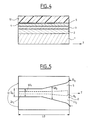
- Figures 4 to 8 show the steps of a manufacturing process of the flared guide semiconductor optical amplifier of FIG. 1.
- the method then comprises a step called masking by a PECVD (Plasma Enhanced Chemical Vapor Deposition en English) of a masking layer 12 made of a dielectric material of the type silica on the protective layer 5.
- PECVD Plasma Enhanced Chemical Vapor Deposition en English
- Figure 5 shows a top view of the optical amplifier semiconductor 10 obtained after a partial elimination step of the masking layer 12 so as to create an opening O above the protective layer 5.
- the opening O comprises a first zone Zo 1 having a cross section SO 1 of constant surface.
- the width Io 1 of the constant surface is of the order of 10 ⁇ m.
- the opening O also includes a zone Zo 2 having a cross section SO 2 of increasing surface.
- the width Io 2 of the increasing surface at the edge B of the opening O is of the order of 20 to 50 ⁇ m.
- the length LO of the opening O is substantially greater than the length L of the optical guide G.
- Figure 6 shows a top view of the optical amplifier semiconductor 10 obtained after a step of depositing the layer of containment 6 by MOVPE.
- the confinement layer 6 is selectively deposited on the opening O according to the SAG technique. As the atoms of InP or GaAs do not adhere to the silica, there is a lateral diffusion of the atoms towards the opening O.
- the zone Zo 1 being narrower than the zone Zo 2 , the diffusion is greater in the zone Zo 1 so that the average growth speed V 1 in this zone Zo 1 can be approximately twice as high as the average growth speed V 2.
- v 1 and v 2 are respectively 2 ⁇ m / h, 1 ⁇ m / h at a temperature of the optical semiconductor amplifier of the order of 600 ° C and for a given flux containing In and P or Ga and As.
- the average thicknesses of layer 6 in zones Zo 1 and Zo 2 are equal to approximately 1 ⁇ m and 0.5 ⁇ m.
- the flow of InP or of GaAs a flux comprising A acceptors such as zinc as the flux of diethyl zinc and a flux comprising D donors such as silicon like the silane flow.
- the zinc concentration is almost independent of the growth rate, it is almost identical in zones Zo 1 and Zo 2 .
- the silicon concentration being inversely proportional to the growth rate V 1 , V 2 , it is higher in the zone Zo 2 and is maximum at the level of the edge B.
- the concentration n p in p doping is therefore substantially constant in the region Zo 1 along the axis Z and is equal to approximately 7.10 17 cm -3 .
- the concentration n p has a constant negative gradient in the region Zo 2 , along the axis Z.
- the concentration np at the edge B is approximately of the order of 3.10 17 cm -3 .
- Figure 7 shows a top view of the optical amplifier semiconductor 10 obtained after a step of total removal of the masking layer 12 which is subsequent to the step of depositing the layer of containment 6.
- FIG. 8 shows an elevation view of the semiconductor optical amplifier 10 obtained after a step of partial removal of the confinement layer 6 outside the region R G in order to limit the confinement layer 6 in the optical guide G .
- the invention can also be applied to an optical component semiconductor having a cross-section optical guide constant as well as all categories of semiconductor optical amplifiers : buried ribbon semiconductor optical amplifier, Gain-guided semiconductor optical amplifier and amplifier semiconductor optics with index guidance.
- the invention can also be used in optical components for which the desired current density is not uniform, such as certain components with an interferometric structure of the Mach Zehnder type. Of In this way, the invention can thus replace the solution based on the design of a so-called distributed electrode.
- the shape of the opening O is chosen as a function of the gradients according to the invention desired. This or these gradients can be constants or variables along the chosen direction.
- the cross section or sections of an optical guide of a component semiconductor optics according to the invention can be rectangular or trapezoidal.
Landscapes
- Physics & Mathematics (AREA)
- Condensed Matter Physics & Semiconductors (AREA)
- General Physics & Mathematics (AREA)
- Electromagnetism (AREA)
- Optics & Photonics (AREA)
- Semiconductor Lasers (AREA)
- Optical Integrated Circuits (AREA)
Applications Claiming Priority (2)
| Application Number | Priority Date | Filing Date | Title |
|---|---|---|---|
| FR0111638 | 2001-09-05 | ||
| FR0111638A FR2829306B1 (fr) | 2001-09-05 | 2001-09-05 | Composant optique semiconducteur et procede de fabrication d'un tel composant |
Publications (1)
| Publication Number | Publication Date |
|---|---|
| EP1291990A1 true EP1291990A1 (de) | 2003-03-12 |
Family
ID=8867096
Family Applications (1)
| Application Number | Title | Priority Date | Filing Date |
|---|---|---|---|
| EP02292132A Withdrawn EP1291990A1 (de) | 2001-09-05 | 2002-08-29 | Optischer Halbleiterbauelement und Herstellungsverfahren |
Country Status (4)
| Country | Link |
|---|---|
| US (1) | US6777768B2 (de) |
| EP (1) | EP1291990A1 (de) |
| JP (1) | JP2003142778A (de) |
| FR (1) | FR2829306B1 (de) |
Families Citing this family (10)
| Publication number | Priority date | Publication date | Assignee | Title |
|---|---|---|---|---|
| DE102008014093B4 (de) * | 2007-12-27 | 2020-02-06 | Osram Opto Semiconductors Gmbh | Kantenemittierender Halbleiterlaserchip mit zumindest einer Strombarriere |
| JP4444368B1 (ja) * | 2009-07-30 | 2010-03-31 | 古河電気工業株式会社 | 集積型半導体レーザ素子および半導体レーザモジュールならびに光伝送システム |
| KR102358584B1 (ko) * | 2013-05-22 | 2022-02-04 | 시-위안 왕 | 마이크로구조-증강 흡수 감광성 디바이스 |
| US10700225B2 (en) | 2013-05-22 | 2020-06-30 | W&Wsens Devices, Inc. | Microstructure enhanced absorption photosensitive devices |
| US10468543B2 (en) | 2013-05-22 | 2019-11-05 | W&Wsens Devices, Inc. | Microstructure enhanced absorption photosensitive devices |
| US10446700B2 (en) | 2013-05-22 | 2019-10-15 | W&Wsens Devices, Inc. | Microstructure enhanced absorption photosensitive devices |
| US11121271B2 (en) | 2013-05-22 | 2021-09-14 | W&WSens, Devices, Inc. | Microstructure enhanced absorption photosensitive devices |
| EP3648269B1 (de) * | 2018-11-02 | 2023-04-26 | Huawei Technologies Co., Ltd. | Optischer verstärker |
| US11837838B1 (en) * | 2020-01-31 | 2023-12-05 | Freedom Photonics Llc | Laser having tapered region |
| EP4352839A4 (de) | 2021-06-10 | 2025-05-07 | Freedom Photonics LLC | Entwürfe für laterale stromsteuerung in optischen verstärkern und lasern |
Family Cites Families (5)
| Publication number | Priority date | Publication date | Assignee | Title |
|---|---|---|---|---|
| JP2572082B2 (ja) | 1987-10-28 | 1997-01-16 | 富士写真フイルム株式会社 | 光半導体デバイス |
| US5539571A (en) * | 1992-09-21 | 1996-07-23 | Sdl, Inc. | Differentially pumped optical amplifer and mopa device |
| US5793521A (en) * | 1992-09-21 | 1998-08-11 | Sdl Inc. | Differentially patterned pumped optical semiconductor gain media |
| JP2842292B2 (ja) * | 1994-09-16 | 1998-12-24 | 日本電気株式会社 | 半導体光集積装置および製造方法 |
| US6091755A (en) * | 1997-11-21 | 2000-07-18 | Sdl, Inc. | Optically amplifying semiconductor diodes with curved waveguides for external cavities |
-
2001
- 2001-09-05 FR FR0111638A patent/FR2829306B1/fr not_active Expired - Fee Related
-
2002
- 2002-08-29 EP EP02292132A patent/EP1291990A1/de not_active Withdrawn
- 2002-09-03 JP JP2002257353A patent/JP2003142778A/ja not_active Withdrawn
- 2002-09-04 US US10/233,398 patent/US6777768B2/en not_active Expired - Lifetime
Non-Patent Citations (3)
| Title |
|---|
| COLAS E ET AL: "IN SITU DEFINITION OF SEMICONDUCTOR STRUCTURES BY SELECTIVE AREA GROWTH AND ETCHING", APPLIED PHYSICS LETTERS, AMERICAN INSTITUTE OF PHYSICS. NEW YORK, US, vol. 59, no. 16, 14 October 1991 (1991-10-14), pages 2019 - 2021, XP000257432, ISSN: 0003-6951 * |
| LIOU K-Y ET AL: "HIGH-POWER BROAD-AREA TAPERED AMPLIFIER WITH A MONOLITHICALLY INTEGRATED OUTPUT FOCUSING LENS AT 0.98-UM WAVELENGTH", IEEE JOURNAL OF SELECTED TOPICS IN QUANTUM ELECTRONICS, IEEE SERVICE CENTER, US, vol. 1, no. 2, 1 June 1995 (1995-06-01), pages 165 - 172, XP000521081, ISSN: 1077-260X * |
| WALPOLE J N ET AL: "DIFFRACTION-LIMITED 1.3-MUM-WAVELENGTH TAPERED-GAIN-REGION LASERS WITH >1-W CW OUTPUT POWER", IEEE PHOTONICS TECHNOLOGY LETTERS, IEEE INC. NEW YORK, US, vol. 8, no. 11, 1 November 1996 (1996-11-01), pages 1429 - 1431, XP000632620, ISSN: 1041-1135 * |
Also Published As
| Publication number | Publication date |
|---|---|
| JP2003142778A (ja) | 2003-05-16 |
| FR2829306A1 (fr) | 2003-03-07 |
| US20030042477A1 (en) | 2003-03-06 |
| FR2829306B1 (fr) | 2003-12-19 |
| US6777768B2 (en) | 2004-08-17 |
Similar Documents
| Publication | Publication Date | Title |
|---|---|---|
| EP2411863B1 (de) | Aus Silizium auf einem Isolator bestehender optischer Breitbandmodulator | |
| EP0458688B1 (de) | Herstellungsverfahren einer integrierten Halbleiter-Lichtleiter-Lichtdetektor-Struktur | |
| EP0511913B1 (de) | Optoelektronisches Element mit integriertem optischem Wellenleiter und Detektor | |
| EP0545808B1 (de) | Optoelektronische Vorrichtung mit sehr niedrigem Serienwiderstand | |
| EP0645654B1 (de) | Verfahren zum Herstellen einer monolitisch integrierten Struktur mit optoelektronischen Komponenten und so hergestellte Strukturen | |
| FR3060772A1 (fr) | Circuit photonique integre optimise | |
| EP1291990A1 (de) | Optischer Halbleiterbauelement und Herstellungsverfahren | |
| FR2695761A1 (fr) | Procédé de fabrication de dispositifs électro-optiques à ruban, notamment de lasers, et dispositifs ainsi obtenus. | |
| EP3353818A1 (de) | Fotodetektor mit einem stapel aus vertikal angrenzenden schichten | |
| EP0664588A1 (de) | Halbleiterstruktur mit virtuellem Beugungsgitter | |
| EP0915543A1 (de) | Optische halbleiterverstärker und integrierte laserquelle | |
| EP0218518B1 (de) | Verfahren zur Herstellung eines Halbleiterlasers mit vergrabener Streifenstruktur mit oder ohne Beugungsgitter und nach diesem Verfahren hergestellter Laser | |
| FR2786279A1 (fr) | Composant optique a base d'amplificateurs optiques a semi-conducteur comportant un nombre reduit d'electrodes independantes | |
| EP1306945A1 (de) | Optische Halbleitervorrichtung und Herstellungsverfahren | |
| FR2749447A1 (fr) | Dispositif optique a guide de lumiere semi-conducteur, a faisceau emergent de faible divergence, application aux lasers de fabry-perot et a contre-reaction distribuee | |
| FR2701165A1 (fr) | Procédé de fabrication d'un composant semi-conducteur notamment d'un laser a arête enterrée, et composant fabriqué par ce procédé. | |
| FR2854469A1 (fr) | Procede de fabrication d'un dispositif optique semi-conducteur comportant une region munie d'une couche active a epaisseur variable | |
| EP1318582A1 (de) | Halbleiterlaser | |
| WO2025008545A1 (fr) | Puce photonique à structure hétérogène de semi-conducteur iii-v sur un deuxième semi-conducteur | |
| FR2485823A1 (fr) | Laser semi-conducteur | |
| EP0508878A1 (de) | Verfahren zur Herstellung von optoelektronischen Halbleiter-Vorrichtungen | |
| FR2813450A1 (fr) | Amplificateur optique en semi-conducteur | |
| FR3167247A1 (fr) | Dispositif photonique III-V intégré sur silicium | |
| WO2021058689A1 (fr) | Miroir de bragg et procédé de réalisation d'un miroir de bragg | |
| FR3120473A1 (fr) | Dispositif opto-électronique à semi-conducteurs |
Legal Events
| Date | Code | Title | Description |
|---|---|---|---|
| PUAI | Public reference made under article 153(3) epc to a published international application that has entered the european phase |
Free format text: ORIGINAL CODE: 0009012 |
|
| AK | Designated contracting states |
Kind code of ref document: A1 Designated state(s): AT BE BG CH CY CZ DE DK EE ES FI FR GB GR IE IT LI LU MC NL PT SE SK TR Designated state(s): AT BE BG CH CY CZ DE DK EE ES FI FR GB GR IE IT LI LU MC NL PT SE SK TR |
|
| AX | Request for extension of the european patent |
Extension state: AL LT LV MK RO SI |
|
| 17P | Request for examination filed |
Effective date: 20030911 |
|
| AKX | Designation fees paid |
Designated state(s): AT BE BG CH CY CZ DE DK EE ES FI FR GB GR IE IT LI LU MC NL PT SE SK TR |
|
| AXX | Extension fees paid |
Extension state: SI Payment date: 20030911 Extension state: RO Payment date: 20030911 Extension state: MK Payment date: 20030911 Extension state: LV Payment date: 20030911 Extension state: LT Payment date: 20030911 Extension state: AL Payment date: 20030911 |
|
| RAP1 | Party data changed (applicant data changed or rights of an application transferred) |
Owner name: AVANEX CORPORATION |
|
| STAA | Information on the status of an ep patent application or granted ep patent |
Free format text: STATUS: THE APPLICATION HAS BEEN WITHDRAWN |
|
| 18W | Application withdrawn |
Effective date: 20040929 |