EP1291957A2 - Dielectric duplexer - Google Patents
Dielectric duplexer Download PDFInfo
- Publication number
- EP1291957A2 EP1291957A2 EP02256190A EP02256190A EP1291957A2 EP 1291957 A2 EP1291957 A2 EP 1291957A2 EP 02256190 A EP02256190 A EP 02256190A EP 02256190 A EP02256190 A EP 02256190A EP 1291957 A2 EP1291957 A2 EP 1291957A2
- Authority
- EP
- European Patent Office
- Prior art keywords
- terminal pad
- dielectric
- resonators
- face
- hole
- Prior art date
- Legal status (The legal status is an assumption and is not a legal conclusion. Google has not performed a legal analysis and makes no representation as to the accuracy of the status listed.)
- Withdrawn
Links
Images


Classifications
-
- H—ELECTRICITY
- H01—ELECTRIC ELEMENTS
- H01P—WAVEGUIDES; RESONATORS, LINES, OR OTHER DEVICES OF THE WAVEGUIDE TYPE
- H01P1/00—Auxiliary devices
- H01P1/20—Frequency-selective devices, e.g. filters
- H01P1/213—Frequency-selective devices, e.g. filters combining or separating two or more different frequencies
- H01P1/2136—Frequency-selective devices, e.g. filters combining or separating two or more different frequencies using comb or interdigital filters; using cascaded coaxial cavities
Definitions
- the present invention relates to a dielectric duplexer including a plurality of resonators arranged in a row for use in mobile communication devices such as car phones and cellular phones.
- a plurality of resonators are arranged in a row in a dielectric ceramic porcelain block of, for example, porcelain.
- Each of the resonators is formed by coating the internal circumferential surface of a through-hole formed in the dielectric porcelain block with an internal conductor.
- a predetermined external circumferential surface of the dielectric porcelain block is coated with an external conductor.
- the resonators comprise two groups. One group serves as a transmission section, which is coupled with an input terminal pad formed on the predetermined external circumferential surface, separated from the external conductor.
- the other group serves as a reception section, which is coupled with an output terminal pad formed on the predetermined external circumferential surface, separated from the external conductor.
- An antenna terminal pad is formed on a mounting surface of the dielectric duplexer, separated from the external conductor in such a manner as to be coupled with the respective resonators of the transmission section and of the reception section located closest to one another in the row.
- dielectric duplexer that is configured as above and, further, such that the output terminal pad is formed on a side surface of the dielectric porcelain block in order to face the resonators of the reception section in the vicinity of their open ends, whereby the output terminal pad is capacitively coupled with the resonators.
- the above-mentioned dielectric duplexer - which is configured such that the output terminal pad is formed on the side surface of the dielectric porcelain block while being capacitively coupled with the resonators of the reception section - involves the following problem.
- the dielectric duplexer is mounted on a printed circuit board such that the output terminal pad is electrically joined to a predetermined conductive path on the board through soldering. Since the state of a joint between the conductive path and the output terminal pad cannot be visually observed from the outside, the joint involves uncertainty as to electrical and mechanical connection and thus always falls under suspicion when a defect arises at a later stage. Also, since the connected state is invisible, retention strength is not reliable. Therefore, a dielectric duplexer of conventional configuration fails to provide sufficient electrical and mechanical reliability in a mounted state.
- the present invention is to provide a dielectric duplexer providing high electrical and mechanical reliability in a mounted state and facilitating adjustment of coupling capacitance.
- the present invention provides a dielectric duplexer configured such that a plurality of resonators are arranged in a row in a dielectric porcelain block, each of the resonators being formed through coating an internal circumferential surface of a through-hole formed in the dielectric porcelain block with an internal conductor; a predetermined external circumferential surface of the dielectric porcelain block is coated with an external conductor; the resonators are divided into two groups such that one group serves as a transmission section, which is coupled with an input terminal pad formed on the predetermined external circumferential surface, separated from the external conductor, and the other group serves as a reception section, which is coupled with an output terminal pad formed on the predetermined external circumferential surface, separated from the external conductor; and an antenna terminal pad is formed on a mounting surface of the dielectric duplexer separated from the external conductor in such a manner as to be coupled with the innermost resonator of the transmission section and the innermost resonator of the reception section.
- the dielectric duplexer is characterized in that the output terminal pad is formed on a side surface of the dielectric porcelain block in separation from the external conductor in such a manner as to face the vicinity of an open end of a resonator of the reception section, and an extension electrode is extended from the output terminal pad onto an end face of the dielectric porcelain block such that the extension electrode approaches the open end in order to capacitively couple with the resonator.
- the extension electrode extending from the output terminal pad and located on the open end face is disposed to face the resonators of the reception section, a capacitance can be generated between the extension electrode and the internal conductor of the resonator.
- This capacitance can be readily corrected by adjusting the position of the end of the extension electrode. The end position is adjusted by, for example, cutting the end or adding a conductor to the end.
- the extension electrode located on an exposed surface of the dielectric duplexer can be soldered to the predetermined conductive path from the outside.
- the output terminal pad is soldered at the bottom and side surfaces thereof; i.e., the output terminal pad is fillet-soldered. Therefore, the connection between the output terminal pad and the predetermined conductive path can checked externally. Further, since the extension electrode is connected to the predetermined conductive path, the surface of joint is expanded, thereby enhancing retention strength.
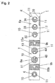
- FIGS. 1 to 3 show a dielectric duplexer 1 in which eight through-holes 5 each coated with an internal conductor are formed in a dielectric ceramic block 2 of, for example, porcelain and having a flat, rectangular parallelepiped shape.
- the through-holes 5 are described from the right: the three rightmost through-holes 5 serve as reception resonators 3A-3C; the fourth through-hole 5 serves as an antenna excitation hole 15a; the subsequent two through-holes 5 serve as transmission resonators 4A and 4B; the seventh through-hole 5 serves as a transmission excitation hole 15b; and the leftmost through-hole 5 serves as a trap formation resonator 6.
- the through-holes 5 are grouped in this manner, whereby the dielectric duplexer 1 is configured such that a group consisting of the three resonators 3A, 3B, and 3C serves as a three-pole-type reception section R, whereas a group consisting of the two resonators 4A and 4B serves as a two-pole-type transmission section T.
- the resonators 3A-3C, 4A, 4B, and 6 substantially assume a length corresponding to ⁇ /4, where ⁇ is a wavelength corresponding to the predetermined resonant frequency.
- the dielectric porcelain block 2 is coated with an external conductor 7 on a predetermined outer circumferential surface thereof.
- the external conductor 7 serves as a shield electrode.
- the resonators 3A-3C, 4A, 4B, and 6 are arranged in a row in the dielectric porcelain block 2.
- a portion of one end face of the dielectric porcelain block 2 serves as an open end 8a, where the external conductor 7 is absent, associated with the resonators, whereas a portion of the opposite end face of the dielectric porcelain block 2 serves as a short circuit end 9a associated with the resonators.
- the antenna excitation hole 15a and the transmission excitation hole 15b assume an interdigital structure in relation to the resonators; specifically, an open end 8b and a short circuit end 9b associated with the excitation holes 15a and 15b are located opposite the open end 8a and the short circuit end 9a associated with the resonators.
- Annular counterbores 10 for coupling adjacent resonators are formed on the open end 8a associated with the resonators 3A-3C, 4A, 4B, and 6 around the corresponding openings.
- An extension conductor 11 is formed on the bottom surface of each of the counterbores 10 and is connected to the corresponding internal conductor.
- An interval between the counterbores 10 is defined as an interval between resonators.
- a coupling capacitance of the resonators can be determined by means of the position, size, and shape of the counterbores 10.
- An antenna terminal pad 13 is formed, separated from the external conductor 7, on a side surface of the dielectric porcelain block 2 in the vicinity of the open end 8b associated with the antenna excitation hole 15a, and is connected to the excitation hole 15a via a connection conductor 16a. In this manner, the antenna terminal pad 13 is coupled via the excitation hole 15a with the respective resonators 3C and 4A of the reception section R and the transmission section T located closest to one another in the row.
- an input terminal pad 12t is formed, separated from the external conductor 7, on a side surface of the dielectric porcelain block 2 in the vicinity of the open end 8b associated with the transmission excitation hole 15b, and is connected to the excitation hole 15b via a connection conductor 16b. In this manner, the input terminal pad 12t is coupled with the transmission section T via the excitation hole 15b.
- the output terminal pad 12r of the reception section R is formed on the mounting surface of the dielectric duplexer 1 separated from the external conductor 7 while the greatest possible distance is established from the above-described antenna terminal pad 13. Specifically, the output terminal pad 12r is formed separated from the external conductor 7 in the vicinity of the open end 8a, which is located on the side opposite the open end 8b, while facing the resonators 3A and 3B located at the endmost position of the reception section R. In this manner, the output terminal pad 12r is capacitively coupled with the reception section R.
- an extension electrode 20 is extended from the output terminal pad 12r onto an end face of the dielectric porcelain block 2 where the open end 8a is located, to thereby be capacitively coupled with the resonators 3A and 3B.
- Formation of the extension electrode 20 in opposition to the resonators 3A and 3B of the reception section R generates capacitance between the extension electrode 20 and the internal electrodes of the resonators 3A and 3B.
- This capacitance can be readily corrected by adjusting the position of the end of the extension electrode 20. Specifically, when the capacitance is excessive, the end is cut. When the capacitance is insufficient, a conductor is added to the end. Since the extension electrode 20 is exposed, this adjustment can be performed even after the dielectric duplexer 1 is mounted on a printed circuit board p, thereby facilitating matching with peripheral devices.
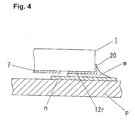
- the dielectric duplexer 1 is mounted on the printed circuit board p such that the input terminal pad 12t, the output terminal pad 12r, and the antenna terminal 13 are electrically, mechanically soldered to corresponding predetermined conductive paths n on a circuit of the printed circuit board p by means of a solder m.
- the input terminal pad 12t is connected to the transmission excitation hole 15b via the connection conductor 16b
- the antenna terminal 13 is connected to the antenna excitation hole 15a via the connection conductor 16a.
- connection inductors 16a and 16b - which are located on an end face of the dielectric porcelain block 2 where the corresponding open ends 8b associated with the excitation holes 15a and 15b are present - are exposed, and the rectangular ends of the connection conductors 16a and 16b are also soldered to the corresponding predetermined conductive paths n by means of the solder m.
- the input terminal pad 12t and the antenna terminal 13 are soldered at the bottom and side surfaces thereof via the connection conductors 16b and 16a, respectively; i.e., each of the input terminal pad 12t and the antenna terminal 13 is fillet-soldered, thereby ensuring electrical and mechanical connections thereof and enabling visibility of the state of connection thereof from the outside.
- the extension electrode 20 extending from the output terminal pad 12r is located on an end face of the dielectric porcelain block 2 while facing the resonators 3A and 3B of the reception section R. Therefore, when the dielectric duplexer 1 is mounted on the printed circuit board p, the extension electrode 20 - which is located on the end face of the block 2 where the open end 8a associated with the resonators 3A and 3B is present - is exposed. Thus, the exposed extension electrode 20 is also soldered to a predetermined conductive path n by means of the solder m.
- the output terminal pad 12r is soldered at the bottom and side surfaces thereof; i.e., the output terminal pad 12r is fillet-soldered, thereby ensuring electrical and mechanical connections thereof to the predetermined conductive path n and enabling visibility of the state of connection thereof from the outside.
- the extension electrode 20 extends from the output terminal pad 12r onto an end face of the dielectric porcelain block where the open end 8a is present, the connection between the output terminal pad 12r and the predetermined conductive path n can be checked from the outside. Further, since the extension electrode 20 is also connected to the predetermined conductive path n, the surface of joint is expanded, thereby enhancing retention strength. Additionally, the input terminal pad 12t, the antenna terminal 13, and the output terminal pad 12r are soldered at the bottom and side surfaces thereof via the connection conductors 16b and 16a and the extension electrode 20, respectively; i.e., each of the input terminal pad 12t, the antenna terminal 13, and the output terminal pad 12r is fillet-soldered. Therefore, the dielectric duplexer 1 as a whole can be enhanced in terms of electrical and mechanical connections, and the state of electrical and mechanical connections can be visually checked, thereby enhancing the reliability of the mounted state of the duplexer.
- the number of resonators to be employed may be varied as appropriate to implement a multiple-type dielectric duplexer.
- the dielectric duplexer of the present invention is configured such that the output terminal pad is formed on a side surface of the dielectric porcelain block separated from the external conductor in such a manner as to face the vicinity of an open end of a resonator of the reception section, and an extension electrode is extended from the output terminal pad onto an end face of the dielectric porcelain block such that the extension electrode approaches the open end in order to capacitively couple with the resonator, thereby yielding the following effects.
Landscapes
- Control Of Motors That Do Not Use Commutators (AREA)
Abstract
Description
Claims (12)
- A dielectric duplexer comprising a dielectric block in which a plurality of resonators are arranged in a row, each of said resonators being formed through coating an internal circumferential surface of a through-hole formed in said dielectric block with an internal conductor, wherein: a predetermined external circumferential surface of said dielectric block is coated with an external conductor; said resonators comprise a first group serving as a transmission section, which is coupled with an input terminal pad formed on the predetermined external circumferential surface separated from the external conductor, and a second group serving as a reception section, which is coupled with an output terminal pad formed on the predetermined external circumferential surface separated from the external conductor; and an antenna terminal pad is formed on a mounting surface of said dielectric duplexer separated from the external conductor in such a manner as to be coupled with said transmission section and said reception section,
said dielectric duplexer being characterized in that said output terminal pad is formed on a side surface of said dielectric block in such a manner as to face the vicinity of an open end of a resonator of said reception section, and an extension electrode is extended from said output terminal pad onto an end face of said dielectric block such that said extension electrode approaches the open end in order to capacitively couple with said resonator of said reception section. - A dielectric duplexer according to claim 1, further including a transmission excitation through-hole formed in said dielectric block at a position to one side of said first group of resonators opposite to the second group of resonators, wherein said input terminal pad is formed on a side surface of said dielectric block in such a manner as to face the vicinity of an open end of the transmission excitation through-hole, and is connected to the transmission excitation through-hole via a connection conductor formed on an end face of said dielectric block where said open end is located whereby said input terminal pad is coupled with the transmission section via the transmission excitation though-hole.
- A dielectric duplexer according to claim 2, wherein said end face at which said open end of said transmission excitation through-hole is located, is opposite the end face onto which said extension electrode is extended.
- A dielectric duplexer according to claim 2 or claim 3, wherein said input terminal pad is formed on the same side surface of said dielectric block as said output terminal pad.
- A dielectric duplexer according to any preceding claim, further including an antenna excitation through-hole formed in said dielectric block at a position between said first group of resonators and said second group of resonators, wherein said antenna terminal pad is formed on a side surface of said dielectric block in such a manner as to face the vicinity of an open end of the antenna excitation through-hole, and is connected to the antenna excitation through-hole via a connection conductor formed on an end face of said dielectric block where said open end is located, whereby said antenna terminal pad is coupled with both said reception section and said transmission section via the antenna excitation through-hole.
- A dielectric duplexer according to claim 5, wherein said end face at which said open end of said antenna excitation through-hole is located, is opposite the end face onto which said extension electrode is extended.
- A dielectric duplexer according to claim 5 or claim 6, wherein said antenna terminal pad is formed on the same side surface of said dielectric block as said output terminal pad.
- A dielectric duplexer according to any preceding claim, wherein said antenna terminal pad is formed in such a manner as to be coupled with respective resonators of said transmission and reception sections located closest to one another in said row.
- A dielectric duplexer according to any preceding claim, wherein at an open end of each resonator of said transmission and reception sections there is a counterbore formed in the dielectric block around the opening of the respective through-hole.
- A dielectric duplexer according to claim 9, wherein said open ends of said resonators of said transmission and reception sections are all located at the same said end face of said dielectric block.
- A dielectric duplexer according to any preceding claim, wherein said dielectric block is made of porcelain.
- An assembly comprising a printed circuit board carrying a conductor on a surface thereof, and a dielectric duplexer according to any preceding claim mounted on said surface of said printed circuit board with said output terminal pad facing and electrically connected by a solder connection to said conductor and with said end face and the extension electrode thereon exposed, said extension electrode being soldered by said solder connection to said conductor.
Applications Claiming Priority (2)
| Application Number | Priority Date | Filing Date | Title |
|---|---|---|---|
| JP2001270616 | 2001-09-06 | ||
| JP2001270616A JP2003087010A (en) | 2001-09-06 | 2001-09-06 | Dielectric duplexer |
Publications (2)
| Publication Number | Publication Date |
|---|---|
| EP1291957A2 true EP1291957A2 (en) | 2003-03-12 |
| EP1291957A3 EP1291957A3 (en) | 2004-01-14 |
Family
ID=19096245
Family Applications (1)
| Application Number | Title | Priority Date | Filing Date |
|---|---|---|---|
| EP02256190A Withdrawn EP1291957A3 (en) | 2001-09-06 | 2002-09-06 | Dielectric duplexer |
Country Status (3)
| Country | Link |
|---|---|
| US (1) | US6798316B2 (en) |
| EP (1) | EP1291957A3 (en) |
| JP (1) | JP2003087010A (en) |
Cited By (2)
| Publication number | Priority date | Publication date | Assignee | Title |
|---|---|---|---|---|
| GB2388719A (en) * | 2002-03-29 | 2003-11-19 | Ngk Spark Plug Co | Dielectric component with attenuation adjustment electrode and method of adjusting attenuation characteristics of the same |
| DE202014002232U1 (en) | 2014-03-14 | 2015-07-22 | Jokon Gmbh | Cable connector and cable cap |
Families Citing this family (1)
| Publication number | Priority date | Publication date | Assignee | Title |
|---|---|---|---|---|
| US9046426B1 (en) * | 2012-06-15 | 2015-06-02 | The United States Of America As Represented By The Administrator Of National Aeronautics And Space Administration | Modular apparatus and method for attaching multiple devices |
Family Cites Families (15)
| Publication number | Priority date | Publication date | Assignee | Title |
|---|---|---|---|---|
| JPS594402A (en) | 1982-06-30 | 1984-01-11 | Asahi Chem Ind Co Ltd | Composite hydrophilic membrane |
| JPS62109503A (en) | 1985-11-07 | 1987-05-20 | 浅野 紳一 | Clasp of safety pin |
| US4879533A (en) * | 1988-04-01 | 1989-11-07 | Motorola, Inc. | Surface mount filter with integral transmission line connection |
| US5250916A (en) * | 1992-04-30 | 1993-10-05 | Motorola, Inc. | Multi-passband dielectric filter construction having filter portions with dissimilarly-sized resonators |
| JPH0711002U (en) * | 1993-07-23 | 1995-02-14 | 日本特殊陶業株式会社 | Dielectric filter |
| DE69524673T3 (en) * | 1994-06-16 | 2013-09-12 | Murata Manufacturing Co., Ltd. | Dielectric filter |
| JPH09219605A (en) * | 1996-02-09 | 1997-08-19 | Ngk Spark Plug Co Ltd | Dielectric filter and resonance frequency adjusting method thereof |
| JPH09312506A (en) * | 1996-05-23 | 1997-12-02 | Ngk Spark Plug Co Ltd | Dielectric filter |
| JP3387422B2 (en) * | 1998-08-25 | 2003-03-17 | 株式会社村田製作所 | Antenna duplexer and communication device |
| JP3412533B2 (en) * | 1998-10-20 | 2003-06-03 | 株式会社村田製作所 | Dielectric filter, dielectric duplexer and communication device |
| JP3498649B2 (en) * | 1998-11-13 | 2004-02-16 | 株式会社村田製作所 | Dielectric filter, duplexer and communication device |
| US6507250B1 (en) * | 1999-08-13 | 2003-01-14 | Murata Manufacturing Co. Ltd. | Dielectric filter, dielectric duplexer, and communication equipment |
| KR100340405B1 (en) * | 1999-08-25 | 2002-06-12 | 이형도 | A duplexer dielectric filter |
| JP2001094304A (en) * | 1999-09-17 | 2001-04-06 | Tdk Corp | Dielectric filter and method of manufacturing the same |
| KR100496161B1 (en) * | 2000-01-19 | 2005-06-20 | 한국전자통신연구원 | Dielectric filter having notch pattern |
-
2001
- 2001-09-06 JP JP2001270616A patent/JP2003087010A/en active Pending
-
2002
- 2002-09-06 EP EP02256190A patent/EP1291957A3/en not_active Withdrawn
- 2002-09-06 US US10/235,657 patent/US6798316B2/en not_active Expired - Fee Related
Cited By (4)
| Publication number | Priority date | Publication date | Assignee | Title |
|---|---|---|---|---|
| GB2388719A (en) * | 2002-03-29 | 2003-11-19 | Ngk Spark Plug Co | Dielectric component with attenuation adjustment electrode and method of adjusting attenuation characteristics of the same |
| GB2388719B (en) * | 2002-03-29 | 2005-08-31 | Ngk Spark Plug Co | Dielectric electronic component with attenuation adjustment electrode and method of adjusting attenuation characteristics of the same |
| US6949987B2 (en) | 2002-03-29 | 2005-09-27 | Ngk Spark Plug Co., Ltd | Dielectric electronic component with attenuation adjustment electrode and method of adjusting attenuation characteristics of the same |
| DE202014002232U1 (en) | 2014-03-14 | 2015-07-22 | Jokon Gmbh | Cable connector and cable cap |
Also Published As
| Publication number | Publication date |
|---|---|
| EP1291957A3 (en) | 2004-01-14 |
| JP2003087010A (en) | 2003-03-20 |
| US6798316B2 (en) | 2004-09-28 |
| US20030042996A1 (en) | 2003-03-06 |
Similar Documents
| Publication | Publication Date | Title |
|---|---|---|
| US9583805B2 (en) | RF filter assembly with mounting pins | |
| JP3780416B2 (en) | Dielectric filter mounting structure, dielectric filter device, dielectric duplexer mounting structure, and communication device | |
| JPS61208902A (en) | Mic type dielectric filter | |
| EP0573597A1 (en) | Monolithic ceramic filter or duplexer having surface mount connections and transmission zeroes | |
| KR100642612B1 (en) | Duplexer device | |
| KR100401969B1 (en) | Dielectric filter, dielectric duplexer, and communication apparatus | |
| KR100394805B1 (en) | Dielectric filter, antenna sharing device and communication device | |
| US6798316B2 (en) | Dielectric duplexer | |
| EP1025608B1 (en) | Duplexer with stepped impedance resonators | |
| CN100477519C (en) | Surface acoustic wave filter | |
| US6507250B1 (en) | Dielectric filter, dielectric duplexer, and communication equipment | |
| JPS63306701A (en) | Dielectric filter | |
| WO2016028343A1 (en) | Rf filter assembly with mounting pins | |
| US6573809B1 (en) | Dielectric resonator device, dielectric duplexer, and communication apparatus incorporating same | |
| KR101681899B1 (en) | Dielectric filter | |
| US20240039136A1 (en) | Filter device and radio-frequency front-end circuit equipped with the same | |
| JP2000068717A (en) | Dielectric resonance component, dielectric filter, antenna duplexer, composite filter, and communication device | |
| JPH09181403A (en) | Insulation board for mounting electronic components | |
| KR101670893B1 (en) | Dielectric filter | |
| KR20010001955A (en) | Dielectric filter | |
| KR100199330B1 (en) | Dielectric filter | |
| JPH01125001A (en) | Dielectric filter | |
| JPH03284001A (en) | Dielectric filter | |
| JP2001352270A (en) | High frequency switch module | |
| JPH0865010A (en) | Broadband dielectric filter |
Legal Events
| Date | Code | Title | Description |
|---|---|---|---|
| PUAI | Public reference made under article 153(3) epc to a published international application that has entered the european phase |
Free format text: ORIGINAL CODE: 0009012 |
|
| AK | Designated contracting states |
Kind code of ref document: A2 Designated state(s): AT BE BG CH CY CZ DE DK EE ES FI FR GB GR IE IT LI LU MC NL PT SE SK TR Designated state(s): AT BE BG CH CY CZ DE DK EE ES FI FR GB GR IE IT LI LU MC NL PT SE SK TR |
|
| AX | Request for extension of the european patent |
Extension state: AL LT LV MK RO SI |
|
| PUAL | Search report despatched |
Free format text: ORIGINAL CODE: 0009013 |
|
| AK | Designated contracting states |
Kind code of ref document: A3 Designated state(s): AT BE BG CH CY CZ DE DK EE ES FI FR GB GR IE IT LI LU MC NL PT SE SK TR |
|
| AX | Request for extension of the european patent |
Extension state: AL LT LV MK RO SI |
|
| 17P | Request for examination filed |
Effective date: 20040701 |
|
| 17Q | First examination report despatched |
Effective date: 20040804 |
|
| AKX | Designation fees paid |
Designated state(s): DE FR GB |
|
| GRAP | Despatch of communication of intention to grant a patent |
Free format text: ORIGINAL CODE: EPIDOSNIGR1 |
|
| STAA | Information on the status of an ep patent application or granted ep patent |
Free format text: STATUS: THE APPLICATION IS DEEMED TO BE WITHDRAWN |
|
| 18D | Application deemed to be withdrawn |
Effective date: 20120313 |