BACKGROUND OF THE INVENTION
Technical Field of the Invention
-
The present invention relates generally to the field of planar optical
waveguides. More particularly, the invention relates to planar optical waveguide
apparatus that include an alignment structure to facilitate measuring the position of an
optical waveguide of the apparatus; and to methods for fabricating planar optical
waveguide apparatus.
Description of Related Art
-
Planar optical waveguides include a core, comprising one or more channels of
transparent material, typically glass, embedded in a cladding of another optical
material, typically also glass, that has a refractive index lower than that of the core
material. The difference in refractive index between the core and the cladding allows
light to be guided in the core.
-
In many applications that utilize a planar optical waveguide apparatus, it is
necessary to connect an external component, such as a laser, a detector, optical fibers,
or the like, to the apparatus in such a manner that the component is correctly aligned
with the input or output edge of an optical waveguide in the apparatus so as to
properly couple light into or out of the waveguide.
-
A variety of techniques have been developed and are utilized in the prior art to
achieve this alignment. For example, one frequently used procedure is an active
alignment procedure wherein the component being aligned is moved relative to the
planar optical waveguide apparatus while the coupled power between the component
and an optical waveguide in the apparatus is monitored. Alignment is optimized when
the coupled power is at a maximum value; and, at that time, the component and the
planar optical waveguide apparatus are connected together.
-
While an active alignment procedure can be effective in many applications, it
is not always practical, or even possible, to connect the component to the planar
optical waveguide apparatus while light is going through the system. For example, if
the component being aligned is a laser, and if the planar optical waveguide apparatus
will be subjected to a high temperature during soldering of the component to the
apparatus; the laser cannot be turned on during the soldering process.
-
Another common alignment procedure involves measuring the position of the
input or output edge of the optical waveguide relative to the position of the
component that is to be aligned with the optical waveguide, and then setting and
fixing the position of the planar optical waveguide apparatus to the desired values.
This procedure, however, requires that the position of the input or output edge of the
optical waveguide be precisely measured in x, y and z directions; and these
measurements are normally rather difficult to achieve.
-
In particular, Fig. 1 is a top plan view and Fig. 2 is an end plan view
schematically illustrating a planar optical waveguide apparatus that is known in the
prior art. The apparatus is generally designated by reference number 10 and comprises
a substrate 11, a lower cladding layer 12, a core layer 13 and an upper cladding layer
14. The core layer is formed from a suitable transparent optical material, usually
glass; and the cladding layers are formed of another optical material, also usually
glass, having a lower refractive index than that of the core layer material. The
substrate often comprises silicon.
-
The difference in refractive index between the material of the core layer and
the cladding layers permits light to be transmitted through the core layer; and by
forming the core layer 13 into a waveguide, as illustrated in Figs. 1 and 2, it is
possible to guide light through the apparatus.
-
With reference to Fig. 1, optical waveguide 13 extends through apparatus 10
from input end 15 thereof to output end 16 such that light entering the waveguide 13
at input end 15 is guided through the apparatus and exits the waveguide at output end
16. The light may be input into the waveguide 13 from a first external component,
generally designated by reference number 17; and may be output from the waveguide
13 to a second external component, generally designated by reference number 18. The
external components 17 and 18 may be connected to the apparatus 10 as
schematically illustrated at 19 in Fig. 1.
-
In order for the planar optical waveguide apparatus 10 to properly transmit
light from component 17 to component 18, input and output edges 15a and 16a of the
optical waveguide 13 must be precisely aligned relative to the components 17 and 18,
respectively; and to achieve proper alignment, it is necessary that the positions of the
edges 15a and 16a of the waveguide 13 be accurately known in x, y and z directions.
-
The x-position of the optical waveguide is the position of the optical
waveguide in the x-direction illustrated by arrow x in Figs. 1 and 2; i.e., the lateral
position of the optical waveguide. The y-position of the optical waveguide is the
position of the waveguide in the y-direction illustrated by the arrow y in Fig. 1; i.e.,
the direction perpendicular to the input or output edge of the optical waveguide and
that defines the spacing between the input or output edge of the optical waveguide and
the component being aligned therewith. The z-position of the optical waveguide is the
position of the waveguide in the z-direction illustrated by the arrow z in Figs. 2; i.e,
the height of the optical waveguide.
-
By knowing the position of the external component 17 or 18, and by knowing
the x, y and z positions of the optical waveguide, the planar optical waveguide
apparatus and the component can be properly positioned relative to one another.
-
The position of the external component 17 or 18 is determined utilizing
suitable indicia provided on the component. The x and y and z positions of the edges
of the optical waveguide are determined by detecting and measuring the positions of
features of the optical waveguide itself. Specifically, to measure the x and y positions
of the edges of the optical waveguide, an image of the optical waveguide is made in a
plane of the waveguide apparatus. Inasmuch, however, as the difference between the
refractive index of the core material forming the waveguide and the refractive index
of the cladding material is normally quite small; attempts to image the waveguide
result in a low contrast image, making precise measurements difficult. The z position
of the edges of the optical waveguide are usually measured using light reflected from
either the upper or lower surface of the waveguide. Again, since the index difference
between the core and cladding materials is quite small; very little light will be
reflected from the surface, making it difficult to accurately measure the z position of
the edges of the waveguide.
-
What is needed is a method and apparatus that facilitates accurate
measurement of the x, y and z positions of the input or output edge of the optical
waveguide in a planar optical waveguide apparatus.
SUMMARY OF THE INVENTION
-
The present invention provides a planar optical waveguide apparatus that
includes alignment structure to facilitate measuring the position of an optical
waveguide of the apparatus.
-
A planar optical waveguide apparatus of the present invention comprises a
core layer and a cladding layer, the core layer including at least one optical
waveguide. In addition, the apparatus includes an alignment structure that is spaced
from and positioned with respect to the at least one optical waveguide to facilitate
measuring a position of the at least one optical waveguide.
-
A planar optical waveguide apparatus according to the present invention
addresses the difficulty in the prior art of accurately measuring the position of an
optical waveguide in the apparatus. According to an embodiment of the invention, the
position of an optical waveguide in a planar optical waveguide apparatus can be
accurately measured by providing alignment structure in the apparatus that is spaced
from and precisely positioned with respect to the waveguide The present invention
permits the position of an optical waveguide to be measured more easily and with
greater accuracy to, in turn, permit an input edge and/or an output edge of the optical
waveguide to be more accurately aligned relative to an external component.
-
According to one embodiment of the invention, the alignment structure
includes a first alignment structure to facilitate measuring a z position of an optical
waveguide of the apparatus; and a second alignment structure to facilitate measuring x
and y positions of the optical waveguide in a plane of the apparatus. The first
alignment structure preferably comprises a reflecting member positioned with respect
to the upper or lower surface of the optical waveguide, and capable of reflecting
sufficient light to permit the z position of the waveguide to be accurately measured.
The second alignment structure preferably comprises alignment marks in registration
with the optical waveguide and capable of providing a high contrast image to permit
the x and y positions of the waveguide to be accurately measured. Because the
alignment structure is spaced from the at least one optical waveguide, the structure
will not, in any way, interfere with the light transmission characteristics of the
waveguide.
-
The reflecting member may comprise a thin layer of a reflective material, such
as a layer of metallic material. Alternatively, the reflecting member may comprise a
thin layer of a material, such as silicon, having a high index of refraction relative to
the indices of refraction of the core layer material and the cladding layer material so
as to define a surface from which sufficient light will be reflected. The alignment
marks may include patterns formed in the reflecting layer so as to be easily visible in
an image of the optical waveguide.
-
According to further embodiments of the invention, methods are provided for
fabricating a planar optical waveguide apparatus having an alignment structure
therein. In general, the methods may include simultaneously forming an optical
waveguide of the apparatus and at least a portion of the alignment structure during a
single processing step to ensure accurate registration therebetween. Preferably, the
single processing step comprises simultaneously forming the optical waveguide and at
least a portion of the alignment structure in a single etch process step.
-
Furthermore, the invention provides embodiments with other features and
advantages in addition to or in lieu of those discussed above. Many of these features
and advantages are apparent from the description below with reference to the
following drawings.
BRIEF DESCRIPTION OF THE DRAWINGS
-
- Fig. 1 is a top plan view of a planar optical waveguide apparatus that is known
in the prior art;
- Fig. 2 is an end plan view of the planar optical waveguide apparatus of Fig. 1;
- Fig. 3 is a top plan view schematically illustrating a planar optical waveguide
apparatus according to a first embodiment of the present invention;
- Fig. 4 is a cross-sectional view of the optical waveguide apparatus of Fig. 3
taken along the line 4-4 in Fig. 3 and enlarged somewhat to illustrate details of the
apparatus;
- Fig. 5 is a cross-sectional view schematically illustrating a planar optical
waveguide apparatus according to a second embodiment of the present invention;
- Fig. 6 is a cross-sectional view schematically illustrating a planar optical
waveguide apparatus according to a third embodiment of the present invention;
- Figs. 7A-7C illustrate a method for fabricating a planar optical waveguide
apparatus, such as the apparatus illustrated in Figs. 3 and 4, according to a fourth
embodiment of the present invention;
- Figs. 8A-8C illustrate a method for fabricating a planar optical waveguide
apparatus, such as the apparatus illustrated in Fig. 5, according to a fifth embodiment
of the present invention; and
- Figs. 9A-9D illustrate a method for fabricating a planar optical waveguide
apparatus, such as the apparatus illustrated in Fig. 6, according to a sixth embodiment
of the present invention.
-
DETAILED DESCRIPTION OF EXEMPLARY EMBODIMENTS OF THE
INVENTION
-
Figs. 3 and 4 illustrate a planar optical waveguide apparatus according to a
first embodiment of the present invention. The apparatus is generally designated by
reference number 20, and comprises a substrate 21, a lower cladding layer 22, a core
layer 23, and an upper cladding layer 24. As is known to those skilled in the art, the
core layer 23 is formed from a suitable transparent optical material, usually glass; and
the cladding layers are formed of another optical material, also usually glass, having a
lower refractive index than that of the core layer material. The substrate typically
comprises silicon.
-
The difference in refractive index between the material of the core layer and
the material of the cladding layers permits light to be transmitted through the core
layer; and by forming the core layer into one or more optical waveguides, it becomes
possible to accurately guide light through the apparatus.
-
In the apparatus illustrated in Figs. 3 and 4, the core layer 23 includes an
optical waveguide portion 25 that is capable of transmitting light through the
apparatus; and an alignment structure, generally designated by reference number 26,
to facilitate accurate measurement of the position of the waveguide 25. As described
above, by accurately measuring the position of the optical waveguide, a more accurate
alignment of an external component, such as a laser, a detector, optical fibers, or the
like (not shown in Figs. 3 and 4), to an input edge 36 or an output edge 37 of the
optical waveguide 25 can be achieved so as to more efficiently couple light into or out
of the waveguide.
-
More particularly, as also mentioned above, a common procedure for aligning
an external component to the optical waveguide is to position the component to be
aligned and the input or output edge of the optical waveguide relative to one another
along x, y and z directions; and then set and fix the relative positions to the desired
values. To do this correctly, however, it is necessary that the x, y, and z positions of
the input or output edge of the waveguide be precisely measured. The external
component is typically provided with suitable indicia to enable the position of the
component to be accurately measured; however, accurate measurement of the x, y and
z positions of the edges of the optical waveguide are normally rather difficult to
achieve because the difference between the refractive index of the core material and
the refractive index of the cladding material is quite small.
-
According to the first embodiment of the present invention, however, accurate
measurements of the x, y and z positions of the optical waveguide 25 are facilitated by
providing alignment structure 26 in the planar optical waveguide apparatus.
Preferably, as illustrated in Fig. 3, the alignment structure 26 is provided adjacent
both the input and output ends of the planar optical waveguide apparatus to permit the
positions of the input and output edges 36 and 37 to be accurately measured.
-
In particular, as illustrated in Figs. 3 and 4, alignment structure 26 includes
first alignment structure 27 to facilitate measuring the z position of the optical
waveguide 25 (i.e., the position of the optical waveguide in the z-direction as
illustrated by arrow z in Fig. 4); and second alignment structure 28 to facilitate
measuring the x and y positions of the waveguide (i.e., the positions of the waveguide
in the directions illustrated by arrow x in Figs. 3 and 4 and arrow y in Fig. 3).
-
Alignment structure 27 comprises a reflecting member positioned to be
aligned with the upper surface 32 of the optical waveguide 25, and capable of
reflecting a sufficient amount of light to permit the z position of the waveguide to be
accurately measured. Specifically, the reflecting member 26 will typically reflect
more light than the surfaces defined by the interfaces between the optical waveguide
25 and the cladding layers 22 and 24. This permits accurate measurements to be more
easily obtained.
-
The reflecting member 27 can comprise a thin layer of a reflective material,
such as a layer of a suitable metallic material: or it can comprise a thin layer of a
material, such as silicon, having a higher refractive index than the refractive indices of
the core layer material and the cladding layer material.
-
The reflecting member 27 is located within the planar optical waveguide
apparatus at positions spaced from the optical waveguide 25 so that it will not
interfere with the transmission characteristics of the waveguide, but is precisely
aligned with or otherwise positioned with respect to the upper surface 32 of the
waveguide so that accurate measurements can be made.
-
The second alignment structure 28 comprises a pair of alignment marks
positioned above the core layer and aligned with the optical waveguide 25 so as to
facilitate measuring the x and y positions of the waveguide. Specifically, the
alignment marks 28 are formed of a material that will provide a high contrast image to
permit the x and y positions of the waveguide to be accurately measured. Preferably,
and as shown in Fig. 4, alignment marks 28 are patterned in the reflecting layer 27 so
as to be above the core layer. Most preferably, and as will be described more fully
hereinafter, at least a portion of the alignment structure 26 is formed simultaneously
with the forming of the optical waveguide 25 in a single processing step to ensure that
the marks will be in perfect registration with the waveguide.
-
Fig. 5 illustrates a planar optical waveguide apparatus 40 according to a
second embodiment of the present invention. As in the embodiment of Figs 3 and 4,
planar optical waveguide apparatus 40 includes a substrate 42, a lower cladding layer
44, a core layer 46 and an upper cladding layer 48. Also, as in the embodiment of
Figs. 3 and 4, the core layer 46 includes a waveguide portion 52 and an alignment
structure 54 comprised of a first alignment structure 56 and a second alignment
structure 58. In the embodiment of Fig. 5, however, the first alignment structure 56
comprises a reflecting member located on the upper surface of the lower cladding
layer 44 and positioned to be aligned with the lower surface 60 of the optical
waveguide 52 to facilitate measuring the z position of the waveguide. The alignment
marks comprising the second alignment structure 58 continue to be located just above
the core layer and are precisely positioned with respect to the optical waveguide 52 to
facilitate measuring of the x and y positions of the waveguide. As shown in Fig. 5, the
alignment marks 58 comprise ridges 62 in the core layer having a reflecting layer 64
applied to the top surfaces thereof so as to provide a high contrast image for
measuring the x and y positions of the waveguide. The ridges 62 are preferably
formed simultaneously with the optical waveguide 52 in a single processing step so as
to guarantee proper registration therebetween. As shown in Fig. 5, the alignment
structure 54 is spaced from the waveguide 52 to ensure it will not interfere with the
light transmission characteristics of the waveguide.
-
Fig. 6 illustrates a planar optical waveguide apparatus 70 according to a third
embodiment of the present invention. Apparatus 70 generally comprises a substrate
72, a core layer 74 and an upper cladding layer 76.
-
In the embodiment of Fig. 6, the substrate 72 comprises silica and functions
as the lower cladding layer of the apparatus. The core layer 74 includes an optical
waveguide portion 78 and an alignment structure, generally designated by reference
number 80. The alignment structure 80 includes a first alignment structure 82 and a
second alignment structure 84. The first alignment structure 82 comprises a reflecting
member 85, comprised of a thin layer of silicon, at the lower end of a ridge 83 and
aligned with respect to the lower surface 86 of the optical waveguide 78 to facilitate
measuring the z position of the waveguide. The second alignment structure 84
includes a plurality of alignment marks in the form of ridges 87 aligned with the
waveguide 78 and having thin layers 88 of silicon at their lower ends to facilitate
measuring the x and y positions of the waveguide. The ridges 83 and 87 are formed of
the same material as the optical waveguide 78 and are preferably formed
simultaneously with the optical waveguide in a single processing step so as to
guarantee proper registration therebetween.
-
In the embodiment of Fig. 6, the thin silicon layer 85 functions as the first
alignment structure for facilitating measuring of the z position of the waveguide; and,
the thin silicon layers 88, because they are located at the lower ends of the ridges 87
of the second alignment structure, enhance the visibility of the ridges to facilitate
measuring the x and y positions of the waveguide.
-
The planar optical waveguide apparatus illustrated in Fig. 6 facilitates
attachment of a laser to the apparatus, and is particularly suitable when coupling an
array of lasers to array waveguide multiplexer devices.
-
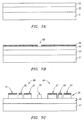
Figs. 7A-7C illustrate a method for fabricating a planar optical waveguide
apparatus, such as the apparatus 10 illustrated in Figs. 3 and 4, according to a further
embodiment of the present invention. Initially, as shown in Fig. 7A, a planar core
layer 92 is provided atop a lower cladding layer 22 that, in turn, is supported on a
substrate 21. Next, a reflecting layer 94 is deposited on top of the core layer; and is
patterned to remove the reflecting layer from the area 96 at which the optical
waveguide 25 will be formed as shown in Fig. 7B.
-
Next, in a single patterning step, both the alignment structure 26 and the
waveguide 25 are formed as shown in Fig. 7C. In an embodiment of the invention, the
patterning step comprises an etch process. The alignment structure is formed by
etching through the reflective layer and the core layer, while the waveguide is formed
by etching through the core layer. By forming the waveguide and the alignment
structure simultaneously in the same etch process step, perfect registration between
the components is guaranteed. Finally, the upper cladding layer 24 (not shown) is
deposited to provide the planar optical waveguide apparatus 10 shown in Fig. 3 and 4.
-
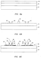
Figs. 8A-8C illustrate a method for fabricating a planar optical waveguide
apparatus, such as the apparatus 40 illustrated in Fig. 5, according to yet a further
embodiment of the present invention. Initially, as in the embodiment illustrated in
Figs. 7A-7C, a core layer 102 is provided atop a lower cladding layer 44 that is
supported on a substrate 42 as shown in Fig. 7A. Next, in a single patterning step,
preferably an etch process step, the waveguide 52 and the ridges 62 of the alignment
marks 58 are formed in the core layer as shown in Fig. 7B. At this time, both the
waveguide and the alignment marks appear as ridges of the core material.
-
Next, a reflective film is deposited and patterned so that the film covers a
portion of the exposed upper surface of the lower cladding layer 44, as shown at 56;
and the ridges 62 of the alignment marks 58, as shown at 64, but not the waveguide
52 as illustrated in Fig. 8C. Finally, the upper cladding layer 48 (not shown) is
deposited to provide the finished planar optical waveguide apparatus 40 illustrated in
Fig. 5.
-
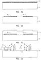
Figs. 9A-9D illustrate a method for fabricating a planar optical waveguide
apparatus such as the apparatus 70 illustrated in Fig. 6. Initially, as shown in Fig. 9A,
a thin layer 110 of silicon is deposited on a silica substrate 72. The silicon layer 110 is
then patterned to clear a space for the waveguide 78. The areas 92 and 94 remain as
shown in Fig. 9B. A layer of material 114, shown in Fig. 9C, is deposited on the
structure of Fig. 9B as the core layer 74. Then, the waveguide 78 and the alignment
structure 80 are patterned in the core layer in a single etching step. Specifically, the
same etching step that etches away the core layer to form the waveguide 78, also
etches through the core layer and the silicon areas 92 and 94 to form the alignment
structure 80. This ensures that the alignment structure will be properly aligned to the
waveguide. As a result of this etching step, the waveguide 78 and alignment structure
are formed as shown in Fig. 9D. The upper cladding layer 76 (not shown) is then
deposited to provide the waveguide apparatus illustrated in Fig. 6.
-
It should be clearly understood that a planar optical waveguide apparatus of
the present invention, such as the embodiments illustrated in Figs. 3-6 can be
fabricated by methods other than those described above. It should also be understood
that the specific embodiments described herein can be varied in many ways without
departing from the scope of the present invention. For example, although the planar
optical waveguide apparatus 10, 40 and 70 described above contain only one optical
waveguide, such apparatus may incorporate a plurality of waveguides; and an
alignment structure of the present invention can also be used to align waveguides in
an apparatus containing a plurality of waveguides. Also, the reflecting members and
the alignment marks could be configured and positioned in different ways as long as
they are appropriately positioned with respect to the waveguides.
-
While what has been described constitutes exemplary embodiments of the
invention, it should be recognized that the invention can be varied in numerous ways
without departing from the scope thereof. Accordingly, it should be recognized that
the invention should be limited only insofar as is required by the scope of the
following claims.