EP1291456A1 - Polycrystalline silicon rod and method for processing the same - Google Patents
Polycrystalline silicon rod and method for processing the same Download PDFInfo
- Publication number
- EP1291456A1 EP1291456A1 EP01934482A EP01934482A EP1291456A1 EP 1291456 A1 EP1291456 A1 EP 1291456A1 EP 01934482 A EP01934482 A EP 01934482A EP 01934482 A EP01934482 A EP 01934482A EP 1291456 A1 EP1291456 A1 EP 1291456A1
- Authority
- EP
- European Patent Office
- Prior art keywords
- rod
- polycrystalline silicon
- central portion
- rods
- slit
- Prior art date
- Legal status (The legal status is an assumption and is not a legal conclusion. Google has not performed a legal analysis and makes no representation as to the accuracy of the status listed.)
- Granted
Links
- 229910021420 polycrystalline silicon Inorganic materials 0.000 title claims abstract description 48
- 238000000034 method Methods 0.000 title claims description 37
- 230000002093 peripheral effect Effects 0.000 claims abstract description 22
- 230000008878 coupling Effects 0.000 claims description 46
- 238000010168 coupling process Methods 0.000 claims description 46
- 238000005859 coupling reaction Methods 0.000 claims description 46
- 230000000149 penetrating effect Effects 0.000 claims description 2
- 238000000137 annealing Methods 0.000 abstract description 10
- 238000002844 melting Methods 0.000 abstract description 10
- 230000008018 melting Effects 0.000 abstract description 10
- XUIMIQQOPSSXEZ-UHFFFAOYSA-N Silicon Chemical compound [Si] XUIMIQQOPSSXEZ-UHFFFAOYSA-N 0.000 description 42
- 229910052710 silicon Inorganic materials 0.000 description 42
- 239000010703 silicon Substances 0.000 description 42
- 238000010586 diagram Methods 0.000 description 6
- 238000010438 heat treatment Methods 0.000 description 6
- 230000006835 compression Effects 0.000 description 5
- 238000007906 compression Methods 0.000 description 5
- 238000011109 contamination Methods 0.000 description 4
- 230000007423 decrease Effects 0.000 description 4
- 229910003460 diamond Inorganic materials 0.000 description 4
- 239000010432 diamond Substances 0.000 description 4
- 239000002184 metal Substances 0.000 description 4
- 229910052751 metal Inorganic materials 0.000 description 4
- 239000002994 raw material Substances 0.000 description 4
- 239000013078 crystal Substances 0.000 description 3
- 150000002739 metals Chemical class 0.000 description 3
- 229910021421 monocrystalline silicon Inorganic materials 0.000 description 3
- ZDHXKXAHOVTTAH-UHFFFAOYSA-N trichlorosilane Chemical compound Cl[SiH](Cl)Cl ZDHXKXAHOVTTAH-UHFFFAOYSA-N 0.000 description 3
- 239000005052 trichlorosilane Substances 0.000 description 3
- UFHFLCQGNIYNRP-UHFFFAOYSA-N Hydrogen Chemical compound [H][H] UFHFLCQGNIYNRP-UHFFFAOYSA-N 0.000 description 2
- 238000006243 chemical reaction Methods 0.000 description 2
- 239000001257 hydrogen Substances 0.000 description 2
- 229910052739 hydrogen Inorganic materials 0.000 description 2
- 239000000155 melt Substances 0.000 description 2
- 239000011248 coating agent Substances 0.000 description 1
- 238000000576 coating method Methods 0.000 description 1
- 238000004891 communication Methods 0.000 description 1
- 230000003247 decreasing effect Effects 0.000 description 1
- 230000007547 defect Effects 0.000 description 1
- 238000000151 deposition Methods 0.000 description 1
- 239000007789 gas Substances 0.000 description 1
- 230000000977 initiatory effect Effects 0.000 description 1
- 238000003672 processing method Methods 0.000 description 1
- SBEQWOXEGHQIMW-UHFFFAOYSA-N silicon Chemical compound [Si].[Si] SBEQWOXEGHQIMW-UHFFFAOYSA-N 0.000 description 1
- 238000004804 winding Methods 0.000 description 1
Images



Classifications
-
- C—CHEMISTRY; METALLURGY
- C30—CRYSTAL GROWTH
- C30B—SINGLE-CRYSTAL GROWTH; UNIDIRECTIONAL SOLIDIFICATION OF EUTECTIC MATERIAL OR UNIDIRECTIONAL DEMIXING OF EUTECTOID MATERIAL; REFINING BY ZONE-MELTING OF MATERIAL; PRODUCTION OF A HOMOGENEOUS POLYCRYSTALLINE MATERIAL WITH DEFINED STRUCTURE; SINGLE CRYSTALS OR HOMOGENEOUS POLYCRYSTALLINE MATERIAL WITH DEFINED STRUCTURE; AFTER-TREATMENT OF SINGLE CRYSTALS OR A HOMOGENEOUS POLYCRYSTALLINE MATERIAL WITH DEFINED STRUCTURE; APPARATUS THEREFOR
- C30B29/00—Single crystals or homogeneous polycrystalline material with defined structure characterised by the material or by their shape
- C30B29/02—Elements
- C30B29/06—Silicon
-
- C—CHEMISTRY; METALLURGY
- C30—CRYSTAL GROWTH
- C30B—SINGLE-CRYSTAL GROWTH; UNIDIRECTIONAL SOLIDIFICATION OF EUTECTIC MATERIAL OR UNIDIRECTIONAL DEMIXING OF EUTECTOID MATERIAL; REFINING BY ZONE-MELTING OF MATERIAL; PRODUCTION OF A HOMOGENEOUS POLYCRYSTALLINE MATERIAL WITH DEFINED STRUCTURE; SINGLE CRYSTALS OR HOMOGENEOUS POLYCRYSTALLINE MATERIAL WITH DEFINED STRUCTURE; AFTER-TREATMENT OF SINGLE CRYSTALS OR A HOMOGENEOUS POLYCRYSTALLINE MATERIAL WITH DEFINED STRUCTURE; APPARATUS THEREFOR
- C30B13/00—Single-crystal growth by zone-melting; Refining by zone-melting
-
- C—CHEMISTRY; METALLURGY
- C30—CRYSTAL GROWTH
- C30B—SINGLE-CRYSTAL GROWTH; UNIDIRECTIONAL SOLIDIFICATION OF EUTECTIC MATERIAL OR UNIDIRECTIONAL DEMIXING OF EUTECTOID MATERIAL; REFINING BY ZONE-MELTING OF MATERIAL; PRODUCTION OF A HOMOGENEOUS POLYCRYSTALLINE MATERIAL WITH DEFINED STRUCTURE; SINGLE CRYSTALS OR HOMOGENEOUS POLYCRYSTALLINE MATERIAL WITH DEFINED STRUCTURE; AFTER-TREATMENT OF SINGLE CRYSTALS OR A HOMOGENEOUS POLYCRYSTALLINE MATERIAL WITH DEFINED STRUCTURE; APPARATUS THEREFOR
- C30B15/00—Single-crystal growth by pulling from a melt, e.g. Czochralski method
- C30B15/02—Single-crystal growth by pulling from a melt, e.g. Czochralski method adding crystallising materials or reactants forming it in situ to the melt
-
- Y—GENERAL TAGGING OF NEW TECHNOLOGICAL DEVELOPMENTS; GENERAL TAGGING OF CROSS-SECTIONAL TECHNOLOGIES SPANNING OVER SEVERAL SECTIONS OF THE IPC; TECHNICAL SUBJECTS COVERED BY FORMER USPC CROSS-REFERENCE ART COLLECTIONS [XRACs] AND DIGESTS
- Y10—TECHNICAL SUBJECTS COVERED BY FORMER USPC
- Y10S—TECHNICAL SUBJECTS COVERED BY FORMER USPC CROSS-REFERENCE ART COLLECTIONS [XRACs] AND DIGESTS
- Y10S117/00—Single-crystal, oriented-crystal, and epitaxy growth processes; non-coating apparatus therefor
- Y10S117/90—Apparatus characterized by composition or treatment thereof, e.g. surface finish, surface coating
-
- Y—GENERAL TAGGING OF NEW TECHNOLOGICAL DEVELOPMENTS; GENERAL TAGGING OF CROSS-SECTIONAL TECHNOLOGIES SPANNING OVER SEVERAL SECTIONS OF THE IPC; TECHNICAL SUBJECTS COVERED BY FORMER USPC CROSS-REFERENCE ART COLLECTIONS [XRACs] AND DIGESTS
- Y10—TECHNICAL SUBJECTS COVERED BY FORMER USPC
- Y10S—TECHNICAL SUBJECTS COVERED BY FORMER USPC CROSS-REFERENCE ART COLLECTIONS [XRACs] AND DIGESTS
- Y10S117/00—Single-crystal, oriented-crystal, and epitaxy growth processes; non-coating apparatus therefor
- Y10S117/911—Seed or rod holders
-
- Y—GENERAL TAGGING OF NEW TECHNOLOGICAL DEVELOPMENTS; GENERAL TAGGING OF CROSS-SECTIONAL TECHNOLOGIES SPANNING OVER SEVERAL SECTIONS OF THE IPC; TECHNICAL SUBJECTS COVERED BY FORMER USPC CROSS-REFERENCE ART COLLECTIONS [XRACs] AND DIGESTS
- Y10—TECHNICAL SUBJECTS COVERED BY FORMER USPC
- Y10T—TECHNICAL SUBJECTS COVERED BY FORMER US CLASSIFICATION
- Y10T117/00—Single-crystal, oriented-crystal, and epitaxy growth processes; non-coating apparatus therefor
- Y10T117/10—Apparatus
- Y10T117/1024—Apparatus for crystallization from liquid or supercritical state
- Y10T117/1032—Seed pulling
-
- Y—GENERAL TAGGING OF NEW TECHNOLOGICAL DEVELOPMENTS; GENERAL TAGGING OF CROSS-SECTIONAL TECHNOLOGIES SPANNING OVER SEVERAL SECTIONS OF THE IPC; TECHNICAL SUBJECTS COVERED BY FORMER USPC CROSS-REFERENCE ART COLLECTIONS [XRACs] AND DIGESTS
- Y10—TECHNICAL SUBJECTS COVERED BY FORMER USPC
- Y10T—TECHNICAL SUBJECTS COVERED BY FORMER US CLASSIFICATION
- Y10T117/00—Single-crystal, oriented-crystal, and epitaxy growth processes; non-coating apparatus therefor
- Y10T117/10—Apparatus
- Y10T117/1024—Apparatus for crystallization from liquid or supercritical state
- Y10T117/1032—Seed pulling
- Y10T117/1072—Seed pulling including details of means providing product movement [e.g., shaft guides, servo means]
-
- Y—GENERAL TAGGING OF NEW TECHNOLOGICAL DEVELOPMENTS; GENERAL TAGGING OF CROSS-SECTIONAL TECHNOLOGIES SPANNING OVER SEVERAL SECTIONS OF THE IPC; TECHNICAL SUBJECTS COVERED BY FORMER USPC CROSS-REFERENCE ART COLLECTIONS [XRACs] AND DIGESTS
- Y10—TECHNICAL SUBJECTS COVERED BY FORMER USPC
- Y10T—TECHNICAL SUBJECTS COVERED BY FORMER US CLASSIFICATION
- Y10T428/00—Stock material or miscellaneous articles
- Y10T428/29—Coated or structually defined flake, particle, cell, strand, strand portion, rod, filament, macroscopic fiber or mass thereof
- Y10T428/2913—Rod, strand, filament or fiber
- Y10T428/2973—Particular cross section
Definitions
- the present invention relates to a polycrystalline silicon rod having a coupling structure and to a method of processing the same. More particularly, the present invention relates to a polycrystalline silicon rod having a structure that enables hanging of polycrystalline silicon rods to each other end-to-end safely and easily, and to a method of processing such polycrystalline silicon rods, in which groove-forming etc. can be made stably without performing annealing treatment.
- polycrystalline silicon rod may sometimes be abbreviated simply as a silicon rod including both of them.
- monocrystalline silicon is produced mainly by the Czhochralski process (CZ process).
- CZ process dips a seed crystal in a melt composed of molten polycrystalline silicon to allow monocrystalline silicon to grow around the seed crystal while drawing up the seed crystal gradually in accordance with the growth to produce a monocrystalline silicon rod.
- the raw material polycrystalline silicon is cut into cylinders of about 70 cm in length, and the mass (called silicon rods) is charged in a crucible for melting and is molten therein.
- silicon rods the mass
- it is generally performed to suspend a silicon rod and introduce it into the remainder of a melt.
- a silicon rod provided with a groove on the periphery thereof near its top is suspended by engaging it with a wire in the groove.
- the rod excluding the upper portion thereof, i.e., from a position several centimeters below the groove to the top of the rod is molten, so that the efficiency of melting is insufficient.
- each of the steps of attaching a wire to the rod, charging the rod into a silicon melt, and drawing up the remaining part of the rod must be repeated several times. This disadvantageously decreases the efficiency of melting operation considerably.
- a process for simultaneously suspending a plurality of silicon rods has been proposed (cf. JP-A-09-255467).
- this process has the problem of instability since it uses a coupling member that is inserted from outside in the groove on the rod on its top to engage it therein so that the coupling member could be disengaged when it would happen to be in contact with the exterior when the coupled rods are being transported or fitted to the melting apparatus.
- annealing treatment intended to decrease residual stress must be practiced to the rod in order to process it without damages.
- a polycrystalline silicon rod is produced from trichlorosilane and hydrogen as the raw materials by the Siemens method, a temperature difference of 100°C or more occurs between the central part of the rod and the surface part of the rod. This causes a difference in stress between the central part and the surface part, which difference in stress remains in the rod as residual stress after completion of the reaction. Accordingly, if the rod is processed to provide therein a groove without performing annealing treatment in advance, cracks tend to occur in the rod by residual stress, thereby damaging the processed portion of the rod.
- the annealing treatment needs heating at about 1,200°C, which is not only troublesome but also requires of an appliance that can afford to practice high temperature heating.
- the present invention is devoted to solve such problems as described above, and an object of the present invention is to provide a structure that can enable stable and easy hanging silicon rods each other.
- Another object of the present invention is to provide a method of processing silicon rods in a stable manner without performing annealing treatment when such a coupling structure is to be processed.
- the present invention provides a silicon rod having the following structure and method of processing it.
- a polycrystalline silicon rod according to the present invention has a structure for hanging of polycrystalline silicon rods to each other end-to-end, wherein an engaging groove is formed on at least one end face of the rods facing to each other, the engaging groove being defined by a slit having a narrow width and an inner space larger than the width of the slit, being open on an end face of the rod and on a side face of the rod, and being adapted for receiving a coupling member having both end portions larger than the width of the slit, whereby being capable of coupling the rods by fitting the coupling member into the respective engaging grooves of the rods facing to each other. Employment of this coupling structure eliminates a fear that the coupling member easily comes off, and enables to engage the rods with stably and ease.
- a polycrystalline silicon rod can be subjected to groove-forming processing without annealing treatment at high temperature, thereby being capable of preventing the contamination of metals due to the high temperature heating. This makes the apparatus for heating unnecessary, thereby being capable of processing speedily.
- the polycrystalline silicon rod subjected to the processing of the present invention minimizes the contamination of metals to obtain high purity.
- a silicon rod 10 of the present invention is provided with an engaging groove 20 in at least one end portion thereof.
- the engaging groove is constituted by a slit 21 and an inner space 22.
- the slit 21 is a narrow groove, which opens on an end surface 16 and a side surface 17 of rod and extends toward the inside of the rod.
- the inner space 22 is integrally formed in communication with the inwardly extending slit 21.
- the inner space 22 is formed wider in width than that of the groove of the slit 21, so that the space communicating with the rod end surface 16 is formed narrow by the slit 21.
- the inner space 22 at its side end opens on the side surface 17.
- the inner space 22 shown in Fig. 1 is formed in the form of a cylinder.
- the shape of the inner space 22 is not particularly limited thereto.
- the shape of opening on the rod side surface 17 may be polygonal or in the form of a dovetail groove or any other shape as far as its width is greater than the width of the slit.
- the depth (D) of the slit 21, that is, the length of the slit 21 until it reaches the inner space 22 is optional.
- the inner space 22 is cylindrical or in the form of a dovetail groove as shown in Fig.
- the depth (D) of the slit 21 may be set to substantially zero (O) so that a portion of the inner space 22 can directly open on the rod end surface 16.
- the length (L) of the slit 21 and inner space 22 is optional and may be any dimension as far as the coupling member 26 can securely be engaged in the engaging groove 26. Note that, in the example shown in the figure, the length (L) of the slit 21 and inner space 22 is set so that they reach near the axis of the rod 10. However, that length (L) may be set to a dimension so that they can extend horizontally across the rod along a diameter thereof.
- the coupling structure of the present invention may also include the structure in which a portion of the inner space 22 directly opens on the rod end surface 16 or the structure in which the slit or inner space extends through the rod.
- the engaging groove 20 is formed at least one end portion of the silicon rod.
- a silicon rod 18 to be attached to a wire (not shown) suspending a rod of a melting apparatus is provided with a groove 25 for winding a wire around it and with the above-described engaging groove 20 in the lower end portion of the rod.
- a silicon rod 19 to be coupled to the silicon rod 18 is provided with the engaging groove 20 according to the present invention in its upper end portion.
- a coupling member 26 is formed so as to have a greater width on its both end portions 26a and 26b than the width of the slit as is illustrated.
- the end portions 26a and 26b of the coupling member 26 are inserted into the engaging grooves 20, 20 of the silicon rods 18 and 19, respectively, from the openings on the side surfaces thereof to fit them thereinto. This makes the coupling member 26 to be fitted through the openings in the end surfaces of the rods so that it can bridge the both silicon rods.
- the end portions 26a and 26b of the coupling member 26 are made wider than the width of the slit so that the end portions 26a and 26b are engaged in the end portions of the slits against the force exerted in the direction along the axis of the rod (force directed toward the end surface), which prevents the coupling member 26 from coming off from the engaging groove 20.
- the silicon rods can be coupled to each other in a stable manner. Since the engaging groove 20 opens on the rod side surface, the coupling member 26 can be inserted in the engaging groove 20 with ease and also detached therefrom with ease. Furthermore, since the coupling rod 26 is engaged in the inside of the rod, there is no fear that the engaged portion contacts the exterior to be disengaged when the coupled rods are handled.
- Fig. 4 illustrates an example of two silicon rods coupled end-to-end vertically but the coupling structure of the present invention is not limited thereto.
- a plurality of silicon rods can be coupled and suspended as follows. That is, more than two silicon rods are prepared, each of which is provided with the above-described engaging groove 20 on each of the upper and lower end portions of the silicon rod, the silicon rods are coupled end-to-end through the engaging grooves 20. Then, the coupled silicon rods are suspended vertically.
- the coupling structure of the present invention can be advantageously applied to silicon-silicon rods and in this case it is preferred that the coupling member made of silicon be used.
- a plurality of silicon rods can be coupled end-to-end and suspended vertically so that the efficiency of melting polycrystalline silicon can be increased considerably. Since the coupling structure of the present invention is engaged in the inside of the rod, the state of engagement is stable and further, the operation is easy since the coupling member can be inserted for engagement from the side surface of the rod.
- Figs. 5 to 8 are diagrams illustrating the processing process of the present invention.
- Figs. 9 to 11 are cross-sectional view, partial perspective view and plan view, respectively, showing the shape of groove (hole).
- Fig. 12 is a schematic diagram illustrating distribution of residual stress in the rod.
- the processing process of the present invention and the rod subjected thereto are featured by removing a peripheral portion of the polycrystalline rod entirely or partially and subjecting the remaining central portion thereof to processing. More particularly, for example, the peripheral portion of the rod end portion is cut round along the peripheral surface to leave a cylindrical central portion or both shoulder portions of a rod end portion is cut off to leave a protruded strip-like central portion, and then the remaining central portion is processed to provide an engaging groove and the like.
- a polycrystalline silicon rod is produced by the Siemens process, in which trichlorosilane and hydrogen as the raw materials are introduced in a sealed vessel and the raw material gases are contacted with the surface of a silicon seed rod heated to a high temperature by application of electric current to thermally decompose the trichlorosilane, thereby depositing silicon, the central portion of the rod has a temperature higher than that of the surface of the rod, so that there is generated a difference in temperature as large as 100°C or more. This results in a difference in stress between the central portion and the surface portion, which difference remains in the rod as residual stress after completion of the reaction.
- the peripheral portion 10b of the rod 10 is removed along the circumferential direction as shown in Fig. 6 to decrease the tensile stress in the radial direction.
- a part of the peripheral portion of the rod end portion, that is, both shoulder portions 31 of the rod end portion is cut off to decrease the tensile stress in the radial direction.
- the portion to be removed is suitably a portion corresponding to 10 to 60% of the diameter.
- the central portion 10a or 30 left after the removal of the peripheral portion is mostly in the region where a compression stress is exerted, so that it will not be cracked when it is subjected to processing.
- the removed portion of less than 10% of the diameter of the rod is not desirable since the portion of tensile stress remains to such an extent that the influence of tensile stress cannot be excluded sufficiently.
- the removed portion of above 60% is not suitable since the central portion to be further processed is too small.
- FIGs. 5 to 8 An example of processing process is illustrated in Figs. 5 to 8.
- a diamond wheel i.e., a cutter provided with a diamond coating on the periphery
- the rod 10 and wheel 11 are rotated in reverse directions to polish the peripheral portion 10b of the rod 10 to remove it.
- the length of the ground portion 10b in the axial direction may be determined properly depending on the shape and depth of the groove to be processed.
- the method for removing the peripheral portion is not limited to grinding and other methods, for example, a method of cutting off the portion surrounding the peripheral portion using a diamond saw or the like and then optionally grinding the resultant circumferential surface using a diamond wheel to obtain a smooth surface may be used.
- the central portion 10a after the centering is subjected to groove forming processing. More particularly, for example, the central portion 10a is drilled using a drill of a small diameter in the radial direction to bore a hole 14 of a small diameter. This operation is repeated in the axial direction from the upper end surface of the central portion 10a to the lower portion of the ground portion to form a groove (slit) 12 communicating vertically. Then using a drill 15 of larger diameter, a hole 13 is bored on the bottom portion of the groove (slit) 12 extending in the same direction to form an engaging groove 20 including an inner space 13 larger than the groove (slit) 12 and communicating therewith.
- the peripheral portion of the rod end portion may be removed. More particularly, the shoulder portions 31 on the both sides of the upper end portion of the rod 10 are removed to leave a central portion 30.
- an engaging groove 32 In the cut surface of the central portion 30 is provided an engaging groove 32, through which a slit 33 of a narrower width is integrally formed vertically.
- the engaging groove 32 may be provided as passing through the central portion 30 or as is shown in Figs 8, it does not penetrate the central portion 30 but may be formed partway.
- the engaging grooves 20 and 32 are formed by slits 12 and 33 and inner space (hole).
- the passage leading to the upper end surface of the rod is formed by the slits 12 and 33, which are narrower, and the inner space from the bottom portion of the slit to the central portion is formed larger.
- the inner space (hole) opens on the side surface of the rod.
- the inner space of the engaging grooves 20 and 30 are formed cylindrical. However, they may be polygonal or dovetail shape in cross section. Also, any other shapes may be used as far as they are wider than the slits 12 and 33.
- the depth (length to the inside of the engaging groove) and length in the radial direction of the slits 12 and 33 are optional and may be any dimension as far as the coupling member can be firmly fitted in the engaging grooves 20 and 30.
- the border portion between the groove (slit) 12 and the inner space may preferably be of a structure that can prevent damages of a corner portion by providing a taper ⁇ with the corner portion.
- FIG. 10 is an example of the shape of the rod end portion as shown in Fig. 6, in which the engaging groove 20 passes through the central portion 10a of the rod in the radial direction.
- the length of the engaging groove 20 in the radial direction may be partway of the central portion 10a as shown in Fig. 11.
- the engaging grooves 20 and 30 as described above are formed in at least one end portion of the silicon rod 10, or in both opposing end surfaces of a pair of silicon rods butted one against another and the rods are coupled to each other end-to-end by means of a coupling member (not shown) that is fitted in the engaging grooves 20 and 30 and the coupled rods are suspended.
- the coupling member has both ends larger than the width of the slits 12 and 33, and the end portions thereof are inserted in the engaging grooves 20 and 30 in the silicon rods, respectively. Since the end portions of the coupling member are each greater than the width of the slits, the end portions can couple the silicon rods 10 to each other without coming off from the slit groove.
- the coupling member can be inserted in the engaging grooves 20 and 30 with ease and also detached with ease. Furthermore, since the coupling member engages in the inside of the engaging grooves 20 and 30, there is no possibility that the engaged portion will contact the exterior and come off.
- a polycrystalline silicon rod according to present invention has a structure for hanging of polycrystalline silicon rods to each other end-to-end, so that the efficiency of melting polycrystalline silicon can be increased considerably.
- processing for forming grooves for coupling silicon rods made of polycrystalline silicon to each other can be performed without subjecting the silicon rods to annealing treatment so that contamination with metal can be avoided.
- the annealing treatment is unnecessary, the processing process can be simplified considerably so that processing for forming grooves and the like can be performed speedily. Furthermore, no heating appliance for annealing treatment is necessary so that processing costs can be reduced.
Landscapes
- Chemical & Material Sciences (AREA)
- Engineering & Computer Science (AREA)
- Crystallography & Structural Chemistry (AREA)
- Materials Engineering (AREA)
- Metallurgy (AREA)
- Organic Chemistry (AREA)
- Silicon Compounds (AREA)
- Crystals, And After-Treatments Of Crystals (AREA)
- Grinding Of Cylindrical And Plane Surfaces (AREA)
- Processing Of Stones Or Stones Resemblance Materials (AREA)
Abstract
Description
- The present invention relates to a polycrystalline silicon rod having a coupling structure and to a method of processing the same. More particularly, the present invention relates to a polycrystalline silicon rod having a structure that enables hanging of polycrystalline silicon rods to each other end-to-end safely and easily, and to a method of processing such polycrystalline silicon rods, in which groove-forming etc. can be made stably without performing annealing treatment. Hereinafter, the term "polycrystalline silicon rod" may sometimes be abbreviated simply as a silicon rod including both of them.
- Recently, monocrystalline silicon is produced mainly by the Czhochralski process (CZ process). This process dips a seed crystal in a melt composed of molten polycrystalline silicon to allow monocrystalline silicon to grow around the seed crystal while drawing up the seed crystal gradually in accordance with the growth to produce a monocrystalline silicon rod. Usually, in order to facilitate its handling, the raw material polycrystalline silicon is cut into cylinders of about 70 cm in length, and the mass (called silicon rods) is charged in a crucible for melting and is molten therein. In this case, in order to increase the efficiency of melting, it is generally performed to suspend a silicon rod and introduce it into the remainder of a melt.
- Heretofore, a silicon rod provided with a groove on the periphery thereof near its top is suspended by engaging it with a wire in the groove. As a result, the rod excluding the upper portion thereof, i.e., from a position several centimeters below the groove to the top of the rod is molten, so that the efficiency of melting is insufficient. In the case where many silicon rods are to be molten, each of the steps of attaching a wire to the rod, charging the rod into a silicon melt, and drawing up the remaining part of the rod must be repeated several times. This disadvantageously decreases the efficiency of melting operation considerably. To cope with this, a process for simultaneously suspending a plurality of silicon rods has been proposed (cf. JP-A-09-255467). However, this process is not free of the defect in that the upper portion from a position neighboring the groove in the periphery of the rod to its upper end makes a melting loss. In addition, a process is known in which silicon rods are each provided with grooves around its periphery on both upper and lower ends, respectively, two such rods are butted end-to-end, and an annular member having a U-shape cross-section is inserted into the upper and lower grooves to couple the rods to each other (cf. JP-A-08-310892). However, this process has the problem of instability since it uses a coupling member that is inserted from outside in the groove on the rod on its top to engage it therein so that the coupling member could be disengaged when it would happen to be in contact with the exterior when the coupled rods are being transported or fitted to the melting apparatus.
- In the case where a silicon rod made of polycrystalline silicon is processed so as to have a conventional suspending structure in its end portion, annealing treatment intended to decrease residual stress must be practiced to the rod in order to process it without damages. When a polycrystalline silicon rod is produced from trichlorosilane and hydrogen as the raw materials by the Siemens method, a temperature difference of 100°C or more occurs between the central part of the rod and the surface part of the rod. This causes a difference in stress between the central part and the surface part, which difference in stress remains in the rod as residual stress after completion of the reaction. Accordingly, if the rod is processed to provide therein a groove without performing annealing treatment in advance, cracks tend to occur in the rod by residual stress, thereby damaging the processed portion of the rod. On the contrary, if the annealing treatment is practiced, contamination of metals from the heating source occurs unavoidably so that the purity of polycrystalline silicon is decreased. Further, the anneal treatment needs heating at about 1,200°C, which is not only troublesome but also requires of an appliance that can afford to practice high temperature heating.
- The present invention is devoted to solve such problems as described above, and an object of the present invention is to provide a structure that can enable stable and easy hanging silicon rods each other.
- Another object of the present invention is to provide a method of processing silicon rods in a stable manner without performing annealing treatment when such a coupling structure is to be processed.
- That is, the present invention provides a silicon rod having the following structure and method of processing it.
- 1) A polycrystalline silicon rod having a structure for hanging of polycrystalline silicon rods to each other end-to-end, wherein an engaging groove is formed on at least one end face of the rods facing to each other, the engaging groove being defined by a slit having a narrow width and an inner space larger than the width of the slit, being open on an end face of the rod and on a side face of the rod, and being adapted for receiving a coupling member having both end portions larger than the width of the slit, whereby being capable of coupling the rods by fitting the coupling member into the respective engaging grooves of the rods facing to each other.
- 2) A polycrystalline silicon rod obtained by entirely or partially removing a peripheral portion from an end portion of the rod to leave a central portion, and processing the central portion.
- 3) A polycrystalline silicon rod as described in the above item 2), wherein both shoulder portions of the rod end portion are removed to leave a central portion and an engaging grove is formed in the central portion.
- 4) A polycrystalline silicon rod as described in the above item 2), wherein the peripheral portion is removed in an amount corresponding to 10 to 60% of a diameter of the rod end portion.
- 5) A polycrystalline silicon rod having a structure for hanging of polycrystalline silicon rods to each other end-to-end, wherein a peripheral portion of the rod is entirely or partially removed to leave a central portion, and an engaging groove is formed on the central portion, the engaging groove being defined by a slit having a narrow width and an inner space larger than the width of the slit, being open on an end face of the rod and on a side face of the rod, and being adapted for receiving a coupling member having both end portions larger than the width of the slit, whereby being capable of coupling the rods by fitting the coupling member into the respective engaging grooves of the rods facing to each other.
- 6) A polycrystalline silicon rod as described in the above item 1) or 5), wherein the engaging groove has an inner space having a spherical, polygonal or dovetail groove-like shape.
- 7) A method of processing a polycrystalline silicon rod, comprising entirely or partially removing a peripheral portion from an end portion of the rod to leave a central portion, and processing the central portion.
- 8) A method of processing a polycrystalline silicon rod as described in the above item 7), wherein both shoulder portions of a rod end portion are removed to leave the central portion, and an engaging grove penetrating the cross section of the central portion is formed therein.
-
- A polycrystalline silicon rod according to the present invention has a structure for hanging of polycrystalline silicon rods to each other end-to-end, wherein an engaging groove is formed on at least one end face of the rods facing to each other, the engaging groove being defined by a slit having a narrow width and an inner space larger than the width of the slit, being open on an end face of the rod and on a side face of the rod, and being adapted for receiving a coupling member having both end portions larger than the width of the slit, whereby being capable of coupling the rods by fitting the coupling member into the respective engaging grooves of the rods facing to each other. Employment of this coupling structure eliminates a fear that the coupling member easily comes off, and enables to engage the rods with stably and ease.
- Further, according to the processing method of the present invention, a polycrystalline silicon rod can be subjected to groove-forming processing without annealing treatment at high temperature, thereby being capable of preventing the contamination of metals due to the high temperature heating. This makes the apparatus for heating unnecessary, thereby being capable of processing speedily. Thus, the polycrystalline silicon rod subjected to the processing of the present invention minimizes the contamination of metals to obtain high purity.
-
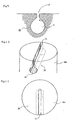
- Fig. 1, Fig. 2, and Fig. 3 are partial views showing appearances of coupling structure portions of a silicon rod; Fig. 4 shows a partial appearance of coupling state of silicon rods, which are coupled vertically.
- Fig. 5 is a diagram illustrating a state initiating a processing process of the present invention; Fig. 6 is a diagram illustrating a procedure of processing process of the present invention; Fig. 7 and Fig. 8 show processes for processing silicon rods to have other shapes according to the present invention, in which Fig. 7 is a schematic appearance of a top end of the rod; Figs. 8 are diagrams showing plane, front and side faces of the rod shown in Fig. 7; Fig. 9 is a cross-sectional view showing an engaging groove processed by the process of the present invention; Fig. 10 shows a perspective appearance of the engaging groove processed by the method of the present invention; Fig. 11 is a plan view showing the engaging groove processed by the method of the present invention; and Fig. 12 is a diagram illustrating distribution of residual stress in the inside of a polycrystalline silicon rod.
-
- Hereinafter, the present invention will be described in detail by embodiments with reference to the attached drawings.
- As illustrated, a
silicon rod 10 of the present invention is provided with anengaging groove 20 in at least one end portion thereof. The engaging groove is constituted by aslit 21 and aninner space 22. Theslit 21 is a narrow groove, which opens on anend surface 16 and aside surface 17 of rod and extends toward the inside of the rod. Theinner space 22 is integrally formed in communication with the inwardly extendingslit 21. Theinner space 22 is formed wider in width than that of the groove of theslit 21, so that the space communicating with therod end surface 16 is formed narrow by theslit 21. Theinner space 22 at its side end opens on theside surface 17. - The
inner space 22 shown in Fig. 1 is formed in the form of a cylinder. However, the shape of theinner space 22 is not particularly limited thereto. As shown in Figs. 2 and 3, the shape of opening on therod side surface 17 may be polygonal or in the form of a dovetail groove or any other shape as far as its width is greater than the width of the slit. The depth (D) of theslit 21, that is, the length of theslit 21 until it reaches theinner space 22 is optional. In the case where theinner space 22 is cylindrical or in the form of a dovetail groove as shown in Fig. 1 or 2, the depth (D) of theslit 21 may be set to substantially zero (O) so that a portion of theinner space 22 can directly open on therod end surface 16. Furthermore, the length (L) of theslit 21 andinner space 22 is optional and may be any dimension as far as thecoupling member 26 can securely be engaged in theengaging groove 26. Note that, in the example shown in the figure, the length (L) of theslit 21 andinner space 22 is set so that they reach near the axis of therod 10. However, that length (L) may be set to a dimension so that they can extend horizontally across the rod along a diameter thereof. Thus, the coupling structure of the present invention may also include the structure in which a portion of theinner space 22 directly opens on therod end surface 16 or the structure in which the slit or inner space extends through the rod. - The
engaging groove 20 is formed at least one end portion of the silicon rod. As shown in Fig. 4, asilicon rod 18 to be attached to a wire (not shown) suspending a rod of a melting apparatus is provided with agroove 25 for winding a wire around it and with the above-describedengaging groove 20 in the lower end portion of the rod. Asilicon rod 19 to be coupled to thesilicon rod 18 is provided with theengaging groove 20 according to the present invention in its upper end portion. Into the engaginggroove 20 is inserted acoupling member 26. Thecoupling member 26 is formed so as to have a greater width on its bothend portions end portions coupling member 26 are inserted into the engaginggrooves silicon rods coupling member 26 to be fitted through the openings in the end surfaces of the rods so that it can bridge the both silicon rods. - The
end portions coupling member 26 are made wider than the width of the slit so that theend portions coupling member 26 from coming off from the engaginggroove 20. As a result, the silicon rods can be coupled to each other in a stable manner. Since the engaginggroove 20 opens on the rod side surface, thecoupling member 26 can be inserted in the engaginggroove 20 with ease and also detached therefrom with ease. Furthermore, since thecoupling rod 26 is engaged in the inside of the rod, there is no fear that the engaged portion contacts the exterior to be disengaged when the coupled rods are handled. - Fig. 4 illustrates an example of two silicon rods coupled end-to-end vertically but the coupling structure of the present invention is not limited thereto. For example, a plurality of silicon rods can be coupled and suspended as follows. That is, more than two silicon rods are prepared, each of which is provided with the above-described
engaging groove 20 on each of the upper and lower end portions of the silicon rod, the silicon rods are coupled end-to-end through the engaginggrooves 20. Then, the coupled silicon rods are suspended vertically. The coupling structure of the present invention can be advantageously applied to silicon-silicon rods and in this case it is preferred that the coupling member made of silicon be used. - By using the above-described coupling structure, a plurality of silicon rods can be coupled end-to-end and suspended vertically so that the efficiency of melting polycrystalline silicon can be increased considerably. Since the coupling structure of the present invention is engaged in the inside of the rod, the state of engagement is stable and further, the operation is easy since the coupling member can be inserted for engagement from the side surface of the rod.
- Next, the processing process of the present invention and the silicon rod subjected to the processing process will be described based on the illustrated embodiment.
- Figs. 5 to 8 are diagrams illustrating the processing process of the present invention. Figs. 9 to 11 are cross-sectional view, partial perspective view and plan view, respectively, showing the shape of groove (hole). Fig. 12 is a schematic diagram illustrating distribution of residual stress in the rod.
- The processing process of the present invention and the rod subjected thereto are featured by removing a peripheral portion of the polycrystalline rod entirely or partially and subjecting the remaining central portion thereof to processing. More particularly, for example, the peripheral portion of the rod end portion is cut round along the peripheral surface to leave a cylindrical central portion or both shoulder portions of a rod end portion is cut off to leave a protruded strip-like central portion, and then the remaining central portion is processed to provide an engaging groove and the like.
- When a polycrystalline silicon rod is produced by the Siemens process, in which trichlorosilane and hydrogen as the raw materials are introduced in a sealed vessel and the raw material gases are contacted with the surface of a silicon seed rod heated to a high temperature by application of electric current to thermally decompose the trichlorosilane, thereby depositing silicon, the central portion of the rod has a temperature higher than that of the surface of the rod, so that there is generated a difference in temperature as large as 100°C or more. This results in a difference in stress between the central portion and the surface portion, which difference remains in the rod as residual stress after completion of the reaction.
- More particularly, as shown in Fig. 12, always a compression stress is exerted in the circumferential direction (direction ), whereas in the radial direction (direction r) a compression stress is exerted in the central portion of the rod but a tensile stress is exerted in the peripheral portion of the rod. On the other hand, in the axial direction (direction z), a tensile stress is exerted in the central portion of the rod but a compression stress is exerted in the peripheral portion of the rod. In the presence of such residual stresses, if the upper end portion of a silicon rod is processed to form a groove, a tensile stress is exerted in the range of the in the radial direction (direction r) so that cracks tend to occur in the radial direction and the rod could be broken easily.
- Accordingly, in the present invention, making the best of the fact that always a compression stress is exerted in the circumferential direction, the peripheral portion 10b of the
rod 10 is removed along the circumferential direction as shown in Fig. 6 to decrease the tensile stress in the radial direction. Alternatively, as shown in Fig. 7, a part of the peripheral portion of the rod end portion, that is, bothshoulder portions 31 of the rod end portion is cut off to decrease the tensile stress in the radial direction. The portion to be removed is suitably a portion corresponding to 10 to 60% of the diameter. Thecentral portion - An example of processing process is illustrated in Figs. 5 to 8. As shown in Fig. 5, a diamond wheel (i.e., a cutter provided with a diamond coating on the periphery) is applied to the periphery at an end portion of the polycrystalline silicon rod (silicon rod) 10. Then the
rod 10 and wheel 11 are rotated in reverse directions to polish the peripheral portion 10b of therod 10 to remove it. The length of the ground portion 10b in the axial direction may be determined properly depending on the shape and depth of the groove to be processed. The method for removing the peripheral portion is not limited to grinding and other methods, for example, a method of cutting off the portion surrounding the peripheral portion using a diamond saw or the like and then optionally grinding the resultant circumferential surface using a diamond wheel to obtain a smooth surface may be used. - Next, the
central portion 10a after the centering is subjected to groove forming processing. More particularly, for example, thecentral portion 10a is drilled using a drill of a small diameter in the radial direction to bore ahole 14 of a small diameter. This operation is repeated in the axial direction from the upper end surface of thecentral portion 10a to the lower portion of the ground portion to form a groove (slit) 12 communicating vertically. Then using adrill 15 of larger diameter, ahole 13 is bored on the bottom portion of the groove (slit) 12 extending in the same direction to form an engaginggroove 20 including aninner space 13 larger than the groove (slit) 12 and communicating therewith. - Furthermore, as shown in Figs. 7 and 8, the peripheral portion of the rod end portion may be removed. More particularly, the
shoulder portions 31 on the both sides of the upper end portion of therod 10 are removed to leave acentral portion 30. In the cut surface of thecentral portion 30 is provided an engaginggroove 32, through which aslit 33 of a narrower width is integrally formed vertically. The engaginggroove 32 may be provided as passing through thecentral portion 30 or as is shown in Figs 8, it does not penetrate thecentral portion 30 but may be formed partway. - As described above, the engaging
grooves slits slits grooves slits slits grooves - What is shown in Fig. 10 is an example of the shape of the rod end portion as shown in Fig. 6, in which the engaging
groove 20 passes through thecentral portion 10a of the rod in the radial direction. The length of the engaginggroove 20 in the radial direction may be partway of thecentral portion 10a as shown in Fig. 11. - The engaging
grooves silicon rod 10, or in both opposing end surfaces of a pair of silicon rods butted one against another and the rods are coupled to each other end-to-end by means of a coupling member (not shown) that is fitted in the engaginggrooves slits grooves silicon rods 10 to each other without coming off from the slit groove. Since the engaginggrooves grooves grooves - A polycrystalline silicon rod according to present invention has a structure for hanging of polycrystalline silicon rods to each other end-to-end, so that the efficiency of melting polycrystalline silicon can be increased considerably. According to the polycrystalline processing process of the present invention and the polycrystalline silicon rod formed by the processing process, processing for forming grooves for coupling silicon rods made of polycrystalline silicon to each other can be performed without subjecting the silicon rods to annealing treatment so that contamination with metal can be avoided. Further, since the annealing treatment is unnecessary, the processing process can be simplified considerably so that processing for forming grooves and the like can be performed speedily. Furthermore, no heating appliance for annealing treatment is necessary so that processing costs can be reduced.
Claims (8)
- A polycrystalline silicon rod having a structure for hanging of polycrystalline silicon rods to each other end-to-end, wherein an engaging groove is formed on at least one end face of the rods facing to each other, the engaging groove being defined by a slit having a narrow width and an inner space larger than the width of the slit, being open on an end face of the rod and on a side face of the rod, and being adapted for receiving a coupling member having both end portions larger than the width of the slit, whereby being capable of coupling the rods by fitting the coupling member into the respective engaging grooves of the rods facing to each other.
- A polycrystalline silicon rod obtained by entirely or partially removing a peripheral portion from an end portion of the rod to leave a central portion, and processing the central portion.
- A polycrystalline silicon rod according to claim 2, wherein both shoulder portions of the rod end portion are removed to leave a central portion and an engaging grove is formed in the central portion.
- A polycrystalline silicon rod according to claim 2, wherein the peripheral portion is removed in an amount corresponding to 10 to 60% of a diameter of the rod end portion.
- A polycrystalline silicon rod having a structure for hanging of polycrystalline silicon rods to each other end-to-end, wherein a peripheral portion of the rod is entirely or partially removed to leave a central portion, and an engaging groove is formed on the central portion, the engaging groove being defined by a slit having a narrow width and an inner space larger than the width of the slit, being open on an end face of the rod and on a side face of the rod, and being adapted for receiving a coupling member having both end portions larger than the width of the slit, whereby being capable of coupling the rods by fitting the coupling member into the respective engaging grooves of the rods facing to each other.
- A polycrystalline silicon rod according to claim 1 or 5, wherein the engaging groove has an inner space having a spherical, polygonal or dovetail groove-like cross sectional shape.
- A method of processing a polycrystalline silicon rod, comprising entirely or partially removing a peripheral portion from an end portion of the rod to leave a central portion, and processing the central portion.
- A method of processing a polycrystalline silicon rod according to claim 7, wherein both shoulder portions of a rod end portion are removed to leave the central portion, and an engaging grove penetrating the cross section of the central portion is formed therein.
Applications Claiming Priority (5)
| Application Number | Priority Date | Filing Date | Title |
|---|---|---|---|
| JP2000167402 | 2000-06-05 | ||
| JP2000167402 | 2000-06-05 | ||
| JP2000214430A JP4661999B2 (en) | 2000-06-05 | 2000-07-14 | Polycrystalline silicon rod and its processing method |
| JP2000214430 | 2000-07-14 | ||
| PCT/JP2001/004636 WO2001094669A1 (en) | 2000-06-05 | 2001-06-01 | Polycrystalline silicon rod and method for processing the same |
Publications (3)
| Publication Number | Publication Date |
|---|---|
| EP1291456A1 true EP1291456A1 (en) | 2003-03-12 |
| EP1291456A4 EP1291456A4 (en) | 2004-10-06 |
| EP1291456B1 EP1291456B1 (en) | 2008-08-20 |
Family
ID=26593306
Family Applications (1)
| Application Number | Title | Priority Date | Filing Date |
|---|---|---|---|
| EP01934482A Expired - Lifetime EP1291456B1 (en) | 2000-06-05 | 2001-06-01 | Polycrystalline silicon rod and method for processing the same |
Country Status (9)
| Country | Link |
|---|---|
| US (2) | US7060355B2 (en) |
| EP (1) | EP1291456B1 (en) |
| JP (1) | JP4661999B2 (en) |
| KR (1) | KR100786049B1 (en) |
| CN (1) | CN1433488A (en) |
| DE (1) | DE60135460D1 (en) |
| MY (1) | MY134229A (en) |
| TW (1) | TWM250934U (en) |
| WO (1) | WO2001094669A1 (en) |
Cited By (2)
| Publication number | Priority date | Publication date | Assignee | Title |
|---|---|---|---|---|
| CN104309016A (en) * | 2014-09-30 | 2015-01-28 | 天津市环欧半导体材料技术有限公司 | Method for processing large-diameter polycrystalline rods |
| WO2017087817A1 (en) * | 2015-11-18 | 2017-05-26 | Sunedison, Inc. | Methods for recycling monocrystalline segments cut from a monocrystalline ingot |
Families Citing this family (5)
| Publication number | Priority date | Publication date | Assignee | Title |
|---|---|---|---|---|
| WO2003042435A1 (en) | 2001-11-13 | 2003-05-22 | Advanced Silicon Materials Llc | System for increasing charge size for single crystal silicon production |
| US8043470B2 (en) * | 2007-11-21 | 2011-10-25 | Lam Research Corporation | Electrode/probe assemblies and plasma processing chambers incorporating the same |
| US9102035B2 (en) * | 2012-03-12 | 2015-08-11 | MEMC Electronics Materials S.p.A. | Method for machining seed rods for use in a chemical vapor deposition polysilicon reactor |
| US9863453B2 (en) | 2013-03-15 | 2018-01-09 | Mitsubishi Polycrystalline Silicon America Corporation (MIPSA) | Mechanical seed coupling |
| CN116024668A (en) * | 2021-10-25 | 2023-04-28 | 天津市环欧半导体材料技术有限公司 | A method for filling gaps in spliced silicon rods |
Family Cites Families (10)
| Publication number | Priority date | Publication date | Assignee | Title |
|---|---|---|---|---|
| JPH08310892A (en) * | 1995-05-16 | 1996-11-26 | Komatsu Electron Metals Co Ltd | Supply blank for production of semiconductor single crystal |
| JPH09255467A (en) * | 1996-03-22 | 1997-09-30 | Sumitomo Sitix Corp | Single crystal raw material supply method and single crystal raw material holder |
| DE69802864T2 (en) * | 1997-05-21 | 2002-08-29 | Shin-Etsu Handotai Co., Ltd. | Silicon seed crystal, method of manufacturing the same, and method of manufacturing a silicon single crystal using the silicon seed crystal |
| JP3376877B2 (en) * | 1997-09-02 | 2003-02-10 | 信越半導体株式会社 | Seed crystal holder |
| JP2000098931A (en) * | 1998-07-24 | 2000-04-07 | Seiko Epson Corp | Display device |
| US6183556B1 (en) * | 1998-10-06 | 2001-02-06 | Seh-America, Inc. | Insulating and warming shield for a seed crystal and seed chuck |
| JP3722264B2 (en) * | 1999-04-27 | 2005-11-30 | 東芝セラミックス株式会社 | Manufacturing method of semiconductor single crystal |
| US6203614B1 (en) * | 1999-05-28 | 2001-03-20 | Memc Electronic Materials, Inc. | Cable assembly for crystal puller |
| JP2001278693A (en) * | 2000-03-31 | 2001-10-10 | Mitsubishi Materials Polycrystalline Silicon Corp | Cut rod joint method and cut rod with joint structure |
| DE10025863A1 (en) * | 2000-05-25 | 2001-12-06 | Wacker Chemie Gmbh | Loaded goods and mounting system for the stored goods |
-
2000
- 2000-07-14 JP JP2000214430A patent/JP4661999B2/en not_active Expired - Lifetime
-
2001
- 2001-05-31 TW TW093206624U patent/TWM250934U/en unknown
- 2001-05-31 MY MYPI20012589 patent/MY134229A/en unknown
- 2001-06-01 CN CN01810701A patent/CN1433488A/en active Pending
- 2001-06-01 EP EP01934482A patent/EP1291456B1/en not_active Expired - Lifetime
- 2001-06-01 US US10/296,230 patent/US7060355B2/en not_active Expired - Lifetime
- 2001-06-01 KR KR1020027016494A patent/KR100786049B1/en not_active Expired - Lifetime
- 2001-06-01 WO PCT/JP2001/004636 patent/WO2001094669A1/en not_active Ceased
- 2001-06-01 DE DE60135460T patent/DE60135460D1/en not_active Expired - Lifetime
-
2006
- 2006-05-01 US US11/414,342 patent/US7455731B2/en not_active Expired - Lifetime
Non-Patent Citations (2)
| Title |
|---|
| No further relevant documents disclosed * |
| See also references of WO0194669A1 * |
Cited By (3)
| Publication number | Priority date | Publication date | Assignee | Title |
|---|---|---|---|---|
| CN104309016A (en) * | 2014-09-30 | 2015-01-28 | 天津市环欧半导体材料技术有限公司 | Method for processing large-diameter polycrystalline rods |
| CN104309016B (en) * | 2014-09-30 | 2016-02-17 | 天津市环欧半导体材料技术有限公司 | A kind of processing method of major diameter polycrystalline bar |
| WO2017087817A1 (en) * | 2015-11-18 | 2017-05-26 | Sunedison, Inc. | Methods for recycling monocrystalline segments cut from a monocrystalline ingot |
Also Published As
| Publication number | Publication date |
|---|---|
| TWM250934U (en) | 2004-11-21 |
| KR100786049B1 (en) | 2007-12-17 |
| EP1291456B1 (en) | 2008-08-20 |
| JP4661999B2 (en) | 2011-03-30 |
| WO2001094669A1 (en) | 2001-12-13 |
| US20030183162A1 (en) | 2003-10-02 |
| CN1433488A (en) | 2003-07-30 |
| US7455731B2 (en) | 2008-11-25 |
| US7060355B2 (en) | 2006-06-13 |
| MY134229A (en) | 2007-11-30 |
| EP1291456A4 (en) | 2004-10-06 |
| DE60135460D1 (en) | 2008-10-02 |
| US20060228565A1 (en) | 2006-10-12 |
| KR20030015265A (en) | 2003-02-20 |
| JP2002059417A (en) | 2002-02-26 |
Similar Documents
| Publication | Publication Date | Title |
|---|---|---|
| EP1291456B1 (en) | Polycrystalline silicon rod and method for processing the same | |
| EP1498516B1 (en) | Single crystal silicon producing method, single crystal silicon wafer and ingot produced thereby | |
| US20120186300A1 (en) | Seed retaining member and method of manufacturing polhycrystalline silicon using the seed retaining member | |
| US6406981B1 (en) | Method for the manufacture of semiconductor devices and circuits | |
| US6444028B2 (en) | Charging material and holding system for the charging material | |
| JP3028767B2 (en) | T-shaped seed crystal and holding jig | |
| EP0792953B1 (en) | Seed crystal holder | |
| JPH09165290A (en) | Graphite crucible for lifting device for semiconductor single crystal and handling method for the same | |
| JP2000169285A (en) | Crucible containing melt | |
| JPH08310892A (en) | Supply blank for production of semiconductor single crystal | |
| KR102728794B1 (en) | Method for growing silicone single crystal | |
| JP2005029434A (en) | Single crystal seed crystal holding member | |
| US10190235B2 (en) | Wafer supporting structure and method for forming the same | |
| JP2001261492A (en) | Method and device for working single crystal | |
| JP2006266813A (en) | Melt collection tool, and ingot manufacturing device using melt collection tool | |
| JP2009234889A (en) | Production method of seed crystal and seed crystal | |
| JPH1171195A (en) | Method of manufacturing split pieces in split graphite crucible | |
| JPS61242983A (en) | Production of semiconductor single crystal rod | |
| JP2008087973A (en) | Single crystal pulling apparatus and single crystal pulling method | |
| KR100486880B1 (en) | Seed and seed chuck of grower silicon single crystal ingot used by Czochralski Method | |
| JP2001278693A (en) | Cut rod joint method and cut rod with joint structure | |
| JP2004018271A (en) | Seed crystal holding fixture and method for producing single crystal | |
| JP3010010B2 (en) | Lifting method of crucible made of carbon fiber reinforced carbon | |
| JP2023535079A (en) | Method for producing monocrystalline silicon ingot by horizontal magnetic field Czochralski | |
| JP2002097096A (en) | Method for working charge rod for single crystal pulling-up |
Legal Events
| Date | Code | Title | Description |
|---|---|---|---|
| PUAI | Public reference made under article 153(3) epc to a published international application that has entered the european phase |
Free format text: ORIGINAL CODE: 0009012 |
|
| 17P | Request for examination filed |
Effective date: 20021128 |
|
| AK | Designated contracting states |
Kind code of ref document: A1 Designated state(s): AT BE CH CY DE DK ES FI FR GB GR IE IT LI LU MC NL PT SE TR |
|
| RBV | Designated contracting states (corrected) |
Designated state(s): AT BE CH DE FI IT LI |
|
| A4 | Supplementary search report drawn up and despatched |
Effective date: 20040819 |
|
| RIC1 | Information provided on ipc code assigned before grant |
Ipc: 7C 30B 29/06 A Ipc: 7C 30B 15/02 B Ipc: 7C 01B 33/02 B Ipc: 7C 30B 15/00 B Ipc: 7C 30B 13/00 B |
|
| 17Q | First examination report despatched |
Effective date: 20050421 |
|
| 17Q | First examination report despatched |
Effective date: 20050421 |
|
| RAP1 | Party data changed (applicant data changed or rights of an application transferred) |
Owner name: MITSUBISHI MATERIALS CORPORATION |
|
| GRAP | Despatch of communication of intention to grant a patent |
Free format text: ORIGINAL CODE: EPIDOSNIGR1 |
|
| GRAS | Grant fee paid |
Free format text: ORIGINAL CODE: EPIDOSNIGR3 |
|
| GRAA | (expected) grant |
Free format text: ORIGINAL CODE: 0009210 |
|
| AK | Designated contracting states |
Kind code of ref document: B1 Designated state(s): DE FI IT |
|
| REF | Corresponds to: |
Ref document number: 60135460 Country of ref document: DE Date of ref document: 20081002 Kind code of ref document: P |
|
| PG25 | Lapsed in a contracting state [announced via postgrant information from national office to epo] |
Ref country code: FI Free format text: LAPSE BECAUSE OF FAILURE TO SUBMIT A TRANSLATION OF THE DESCRIPTION OR TO PAY THE FEE WITHIN THE PRESCRIBED TIME-LIMIT Effective date: 20080820 |
|
| PLBE | No opposition filed within time limit |
Free format text: ORIGINAL CODE: 0009261 |
|
| STAA | Information on the status of an ep patent application or granted ep patent |
Free format text: STATUS: NO OPPOSITION FILED WITHIN TIME LIMIT |
|
| 26N | No opposition filed |
Effective date: 20090525 |
|
| PGFP | Annual fee paid to national office [announced via postgrant information from national office to epo] |
Ref country code: IT Payment date: 20150622 Year of fee payment: 15 |
|
| PG25 | Lapsed in a contracting state [announced via postgrant information from national office to epo] |
Ref country code: IT Free format text: LAPSE BECAUSE OF NON-PAYMENT OF DUE FEES Effective date: 20160601 |
|
| PGFP | Annual fee paid to national office [announced via postgrant information from national office to epo] |
Ref country code: DE Payment date: 20200618 Year of fee payment: 20 |
|
| REG | Reference to a national code |
Ref country code: DE Ref legal event code: R071 Ref document number: 60135460 Country of ref document: DE |