EP1291450A2 - Diamond coated cutting tool and method for making the same - Google Patents
Diamond coated cutting tool and method for making the same Download PDFInfo
- Publication number
- EP1291450A2 EP1291450A2 EP02019797A EP02019797A EP1291450A2 EP 1291450 A2 EP1291450 A2 EP 1291450A2 EP 02019797 A EP02019797 A EP 02019797A EP 02019797 A EP02019797 A EP 02019797A EP 1291450 A2 EP1291450 A2 EP 1291450A2
- Authority
- EP
- European Patent Office
- Prior art keywords
- tungsten carbide
- grain size
- micrometers
- sintered substrate
- carbide grain
- Prior art date
- Legal status (The legal status is an assumption and is not a legal conclusion. Google has not performed a legal analysis and makes no representation as to the accuracy of the status listed.)
- Withdrawn
Links
Images














Classifications
-
- C—CHEMISTRY; METALLURGY
- C23—COATING METALLIC MATERIAL; COATING MATERIAL WITH METALLIC MATERIAL; CHEMICAL SURFACE TREATMENT; DIFFUSION TREATMENT OF METALLIC MATERIAL; COATING BY VACUUM EVAPORATION, BY SPUTTERING, BY ION IMPLANTATION OR BY CHEMICAL VAPOUR DEPOSITION, IN GENERAL; INHIBITING CORROSION OF METALLIC MATERIAL OR INCRUSTATION IN GENERAL
- C23C—COATING METALLIC MATERIAL; COATING MATERIAL WITH METALLIC MATERIAL; SURFACE TREATMENT OF METALLIC MATERIAL BY DIFFUSION INTO THE SURFACE, BY CHEMICAL CONVERSION OR SUBSTITUTION; COATING BY VACUUM EVAPORATION, BY SPUTTERING, BY ION IMPLANTATION OR BY CHEMICAL VAPOUR DEPOSITION, IN GENERAL
- C23C16/00—Chemical coating by decomposition of gaseous compounds, without leaving reaction products of surface material in the coating, i.e. chemical vapour deposition [CVD] processes
- C23C16/02—Pretreatment of the material to be coated
- C23C16/0209—Pretreatment of the material to be coated by heating
-
- B—PERFORMING OPERATIONS; TRANSPORTING
- B22—CASTING; POWDER METALLURGY
- B22F—WORKING METALLIC POWDER; MANUFACTURE OF ARTICLES FROM METALLIC POWDER; MAKING METALLIC POWDER; APPARATUS OR DEVICES SPECIALLY ADAPTED FOR METALLIC POWDER
- B22F7/00—Manufacture of composite layers, workpieces, or articles, comprising metallic powder, by sintering the powder, with or without compacting wherein at least one part is obtained by sintering or compression
- B22F7/06—Manufacture of composite layers, workpieces, or articles, comprising metallic powder, by sintering the powder, with or without compacting wherein at least one part is obtained by sintering or compression of composite workpieces or articles from parts, e.g. to form tipped tools
-
- C—CHEMISTRY; METALLURGY
- C23—COATING METALLIC MATERIAL; COATING MATERIAL WITH METALLIC MATERIAL; CHEMICAL SURFACE TREATMENT; DIFFUSION TREATMENT OF METALLIC MATERIAL; COATING BY VACUUM EVAPORATION, BY SPUTTERING, BY ION IMPLANTATION OR BY CHEMICAL VAPOUR DEPOSITION, IN GENERAL; INHIBITING CORROSION OF METALLIC MATERIAL OR INCRUSTATION IN GENERAL
- C23C—COATING METALLIC MATERIAL; COATING MATERIAL WITH METALLIC MATERIAL; SURFACE TREATMENT OF METALLIC MATERIAL BY DIFFUSION INTO THE SURFACE, BY CHEMICAL CONVERSION OR SUBSTITUTION; COATING BY VACUUM EVAPORATION, BY SPUTTERING, BY ION IMPLANTATION OR BY CHEMICAL VAPOUR DEPOSITION, IN GENERAL
- C23C16/00—Chemical coating by decomposition of gaseous compounds, without leaving reaction products of surface material in the coating, i.e. chemical vapour deposition [CVD] processes
- C23C16/02—Pretreatment of the material to be coated
- C23C16/0227—Pretreatment of the material to be coated by cleaning or etching
-
- C—CHEMISTRY; METALLURGY
- C23—COATING METALLIC MATERIAL; COATING MATERIAL WITH METALLIC MATERIAL; CHEMICAL SURFACE TREATMENT; DIFFUSION TREATMENT OF METALLIC MATERIAL; COATING BY VACUUM EVAPORATION, BY SPUTTERING, BY ION IMPLANTATION OR BY CHEMICAL VAPOUR DEPOSITION, IN GENERAL; INHIBITING CORROSION OF METALLIC MATERIAL OR INCRUSTATION IN GENERAL
- C23C—COATING METALLIC MATERIAL; COATING MATERIAL WITH METALLIC MATERIAL; SURFACE TREATMENT OF METALLIC MATERIAL BY DIFFUSION INTO THE SURFACE, BY CHEMICAL CONVERSION OR SUBSTITUTION; COATING BY VACUUM EVAPORATION, BY SPUTTERING, BY ION IMPLANTATION OR BY CHEMICAL VAPOUR DEPOSITION, IN GENERAL
- C23C16/00—Chemical coating by decomposition of gaseous compounds, without leaving reaction products of surface material in the coating, i.e. chemical vapour deposition [CVD] processes
- C23C16/22—Chemical coating by decomposition of gaseous compounds, without leaving reaction products of surface material in the coating, i.e. chemical vapour deposition [CVD] processes characterised by the deposition of inorganic material, other than metallic material
- C23C16/26—Deposition of carbon only
- C23C16/27—Diamond only
-
- Y—GENERAL TAGGING OF NEW TECHNOLOGICAL DEVELOPMENTS; GENERAL TAGGING OF CROSS-SECTIONAL TECHNOLOGIES SPANNING OVER SEVERAL SECTIONS OF THE IPC; TECHNICAL SUBJECTS COVERED BY FORMER USPC CROSS-REFERENCE ART COLLECTIONS [XRACs] AND DIGESTS
- Y10—TECHNICAL SUBJECTS COVERED BY FORMER USPC
- Y10T—TECHNICAL SUBJECTS COVERED BY FORMER US CLASSIFICATION
- Y10T428/00—Stock material or miscellaneous articles
- Y10T428/25—Web or sheet containing structurally defined element or component and including a second component containing structurally defined particles
- Y10T428/252—Glass or ceramic [i.e., fired or glazed clay, cement, etc.] [porcelain, quartz, etc.]
-
- Y—GENERAL TAGGING OF NEW TECHNOLOGICAL DEVELOPMENTS; GENERAL TAGGING OF CROSS-SECTIONAL TECHNOLOGIES SPANNING OVER SEVERAL SECTIONS OF THE IPC; TECHNICAL SUBJECTS COVERED BY FORMER USPC CROSS-REFERENCE ART COLLECTIONS [XRACs] AND DIGESTS
- Y10—TECHNICAL SUBJECTS COVERED BY FORMER USPC
- Y10T—TECHNICAL SUBJECTS COVERED BY FORMER US CLASSIFICATION
- Y10T428/00—Stock material or miscellaneous articles
- Y10T428/30—Self-sustaining carbon mass or layer with impregnant or other layer
Definitions
- the invention pertains to a coated cutting tool and a method for making the same. More particularly, the invention pertains to a diamond coated cutting tool that has a cemented (cobalt) tungsten carbide substrate and a method for making the same.
- Diamond coated cutting tools demonstrate excellent metalcutting properties in certain circumstances.
- diamond coated cutting tools comprise a substrate of cemented (cobalt) tungsten carbide that has a diamond coating on the surface thereof. It has always been, and still remains, a goal to improve the adhesion of the diamond coating to the substrate.
- U.S. Patent No. 5,585,176 to Grab et al. and U.S. Patent No. 5,648,119 to Grab et al. each shows a diamond coated cutting tool.
- a sintering step or re-sintering step
- grain growth and cobalt i.e., binder
- the magnetic saturation value is a measure of the carbon content in the cobalt binder. Magnetic saturation is generally reported in either microtesla cubic meter per kilogram cobalt ( ⁇ T-m 3 /kg) or gauss cubic centimeter per gram cobalt (gauss-cm 3 /gm).
- ⁇ T-m 3 /kg microtesla cubic meter per kilogram cobalt
- gauss-cm 3 /gm gauss cubic centimeter per gram cobalt
- the magnetic saturation value of the sintered substrates i.e., the substrate prior to re-sintering
- the magnetic saturation value of the sintered substrates must fall within a narrow range.
- a narrow range for the magnetic saturation value is difficult to accurately measure.
- This difficulty in measuring may result in not all of the sintered substrates falling within the prescribed range of the magnetic saturation value which may, in turn, result in re-sintered substrates that have certain drawbacks as described above if the magnetic saturation value is either too high or too low.
- Iron contamination can also affect the magnetic saturation value by causing it to be over reported. This may also result in the re-sintering of sintered substrates that do not have a magnetic saturation value within the prescribed range.
- the grain size of the tungsten carbide in the sintered substrate has been fine.
- the extent of re-sintering has had to be relatively long to achieve tungsten carbide grains with a sufficiently larger grain size in the re-sintered substrate.
- the invention is a process for making a diamond coated cutting tool.
- the process comprising the following steps: providing a sintered substrate, the sintered substrate comprising tungsten carbide and cobalt, the sintered substrate having an average tungsten carbide grain size of between about 3 micrometers and about 20 micrometers; re-sintering the sintered substrate to produce a re-sintered substrate, the re-sintered substrate having a surface; the re-sintered substrate having a surface region beginning at and extending inwardly from the surface, the re-sintered substrate having a bulk region inwardly of the surface region, and the surface region of the re-sintered substrate having an average tungsten carbide grain size of between about 12 micrometers and about 60 micrometers, the bulk region of the re-sintered substrate having an average tungsten carbide grain size of between about 3 micrometers and about 20 micrometers, and wherein the average tungsten carbide grain size in the surface region is greater than the average tungsten
- the invention is a diamond coated cutting tool produced by a process comprising the steps of: providing a sintered substrate, the sintered substrate comprising tungsten carbide and cobalt, the sintered substrate having an average tungsten carbide grain size of between about 3 micrometers and about 20 micrometers; re-sintering the sintered substrate to produce a re-sintered substrate, the re-sintered substrate having a surface; the re-sintered substrate having a surface region beginning at and extending inwardly from the surface, the re-sintered substrate having a bulk region inwardly of the surface region, and the surface region of the re-sintered substrate having an average tungsten carbide grain size of between about 12 micrometers and about 60 micrometers, the bulk region of the re-sintered substrate having an average tungsten carbide grain size of between about 3 micrometers and about 20 micrometers; subjecting the re-sintered substrate to a chemical treatment for the removal of cobalt at the surface
- the invention is a diamond coated cutting tool comprising a re-sintered substrate.
- the re-sintered substrate has a composition comprising between about 2 weight percent to about 12 weight percent cobalt, and tungsten and carbon wherein most of the tungsten and carbon is in the form of tungsten carbide.
- the re-sintered substrate has a surface, and the surface is subjected to a chemical treatment.
- the re-sintered substrate has a surface region extending inwardly from the surface and a bulk region being inwardly of the surface region.
- the surface region has an average tungsten carbide grain size of between about 12 micrometers and about 60 micrometers.
- the bulk region has an average tungsten carbide grain size of between about 3 micrometers about 20 micrometers.
- the average tungsten carbide grain size in the surface region is greater than the average tungsten carbide grain size in the bulk region.
- a diamond coating is on the surface of the re-sintered substrate.
- FIG. 1 illustrates a specific embodiment of a cutting tool generally designated as 20.
- Cutting tool 20 has a top rake surface 22 and flank surfaces 24.
- the top rake surface 22 intersects with the flank surfaces 24 so as to form cutting edges 26 at the intersections.
- cutting tool 20 comprises a treated substrate 30 that has a diamond coating 38 thereon.
- the treated substrate 30 has a surface 32.
- the treated substrate 30 has a surface region 34 that begins at (or near) and extends inwardly from the surface 32.
- the treated substrate 30 further has a bulk region 36 inwardly of the surface region 34.
- the grain size of the tungsten carbide grains in the surface region 34 is different from the grain size of the tungsten carbide grains in the bulk region 36.
- FIG. 2 shows that the diamond coating has been applied to the rake surface and the flank surface(s) of the substrate.
- the coating may only be applied to a selected one or a portion of the surfaces.
- the treated substrate is the resultant article from a re-sintering of a sintered substrate to form a re-sintered substrate.
- the re-sintered substrate is chemically treated (and then optionally subjected to a treatment (called seeding or scratching) of diamond particles suspended in a solvent and agitated ultrasonically) to form the treated substrate.
- the sintered substrate 30 is a cemented (cobalt) tungsten carbide material that does not have any (or at most has minimal) other carbide-forming elements (e.g., tantalum, titanium, niobium, vanadium, zirconium, hafnium, and chromium) therein. More specifically, it is preferable if the total of the titanium, niobium and zirconium is less than 0.2 weight percent. It is even more preferable if the total of these elements is less than 0.1 weight percent. It is the most preferable if the total of these elements is less than 0.01 weight percent.
- carbide-forming elements e.g., tantalum, titanium, niobium, vanadium, zirconium, hafnium, and chromium
- the sintered substrate it is preferable if the following levels of the following elements are present: less than 0.4 weight percent tantalum, less than 0.2 weight percent hafnium, less than 0.1 weight percent chromium, and less than 0.1 weight percent vanadium. It is most preferable if the contents of tantalum, hafnium, chromium, and vanadium is about zero weight percent.
- the sintered substrate it is preferred if less than 0.2 weight percent iron is present and less than 0.2 weight percent nickel is present. It is most preferable if there is an absence of iron and nickel from the treated substrate.
- the sintered substrate has a preferred composition of between about 2 weight percent and 12 weight percent cobalt with the balance being tungsten and carbon wherein most of the tungsten and carbon is in the form of tungsten carbide.
- a more preferred composition for the treated substrate is between about 5.2 weight percent and about 6.5 weight percent cobalt with the balance being tungsten and carbon wherein most of the tungsten and carbon is in the form of tungsten carbide.
- a still more preferred composition for the treated substrate is between about 5.7 weight percent and about 6.2 weight percent cobalt with the balance being tungsten and carbon wherein most of the tungsten and carbon is in the form of tungsten carbide.
- the preferred bulk average grain size of the tungsten carbide in the sintered substrate is between about 3 micrometers and about 20 micrometers as measured according to the technique set forth in Roebuck, B., "Measurement of WC Grain Size", NPL Report CMMT (A)141 page 2 (Jan. 1999).
- a more preferred average bulk grain size of the tungsten carbide is between 7 micrometers and 13 micrometers.
- the substrate was cut, mounted, polished and etched according to ASTM Procedure D657. Then the grain size was measured according to the technique in the Roebuck et al. article.
- one preferred range of the magnetic saturation value is between about 17.3 and about 19.8 microtesla cubic meter per kilogram cobalt.
- Another preferred range of the magnetic saturation value of the sintered substrate is between about 17.8 and about 18.8 microtesla cubic meter per kilogram cobalt.
- the composition of the sintered substrate it is preferred if there is enough free tungsten in the binder to permit grains of tungsten carbide to grow as the cobalt is evaporated during the re-sintering process, and yet, avoid the formation of eta phase.
- the treated substrate 30 has a surface region 34 that extends inwardly from the surface 32 of the treated substrate 30. It is typical that the surface region 34 extends inwardly from the surface 32 a distance of between about 10 micrometers and about 60 micrometers. Oftentimes the depth of the surface region 34 is equal to the average grain size of one tungsten carbide grain.
- the preferred tungsten carbide grain size in the surface region of the treated substrate is between 10 micrometers and 60 micrometers as measured according to the Roebuck et al. technique described above.
- a bulk region 36 of the treated substrate Inwardly of the surface region 34 is a bulk region 36 of the treated substrate.
- the preferred average grain size of the tungsten carbide in the bulk region of the treated substrate is between 3 micrometers and 15 micrometers as measured according to the Roebuck et al. technique described hereinabove. More preferably, the average grain size of the tungsten carbide in the bulk region of the treated substrate is between about 8 micrometers and about 13 micrometers according to the Roebuck et al. technique described hereinabove.
- the porosity rating of the treated substrate it is preferred of there is no C-type porosity in either the surface region of the treated substrate or the bulk region of the treated substrate.
- An acceptable porosity rating according to ASTM Designation B276-91 (Reapproved 1996) is A02+B00+C00 for the surface region, and A02+B00+C00 for the bulk region of the treated substrate.
- the surface roughness, R a of rake surface of the treated substrate, it is preferable that the surface roughness, R a , be greater than about 25 microinches and more preferably be greater than about 35 microinches.
- the surface of the treated substrate exhibits as little as possible residual surface cobalt thereon.
- the ratio (Co/W) of the cobalt peak height (Co-K-alpha) to the tungsten peak height (W-L-alpha) is one way to determine the amount of the residual surface cobalt.
- the portion at the edge of the rake surface adjacent to the nose has a Co/W peak ratio of less than or equal to 0.4, and the center of the rake surface preferably has a Co/W peak ratio of less than or equal to 0.2. Even more preferably, the Co/W peak ratio at either the edge of the rake surface adjacent to the nose or at the center of the rake surface is less than 0.1.
- the average adhesion strength of the diamond coating to the surface of the treated substrate is at least 60 kilograms (kg). More preferably, the adhesion strength is at least 80 kg, and most preferably the adhesion strength is at least 100 kg.
- the test to determine the adhesion strength is a Rockwell A indentation test.
- the diamond coating on the rake surface of a cutting tool preferably has an average thickness of between about 5 micrometers to about 100 micrometers, and more preferably the average thickness is between about 22 micrometers to about 100 micrometers.
- a preferred average thickness of the diamond coating is between about 22 micrometers and about 50 micrometers, and a more preferred range for the average thickness of the diamond coating is between about 35 micrometers and about 50 micrometers.
- the diamond coating applied to the rake surface is left in its as deposited condition so as to have a surface roughness, R a, of greater than about 25 microinches while the diamond coating on the flank surface(s) is made smoother by polishing or the like.
- R a surface roughness
- the surface of the rake surface has a greater surface roughness, R a , than the surface roughness, R a , of the flank surface(s).
- the process to produce the diamond coated cutting tool comprises blending the components of the starting powder to form a powder blend.
- the typical starting powders comprise cobalt powder, tungsten carbide powder and carbon powder to the extent needed to adjust the carbon level in the composition.
- the powder blend generally includes a fugitive binder and lubricant materials.
- the powder blend is then pressed into a green compact.
- the green compact is in the general shape of a cutting tool.
- the green compact is then sintered until it reaches full density so as to form a sintered substrate.
- the sintering takes place at a sintering temperature that ranges between about 2550 degrees Fahrenheit (about 1400 degrees Centigrade) and about 2910 degrees Fahrenheit (about 1600 degrees Centigrade) wherein the preferred sintering temperature equals about 2700 degrees Fahrenheit (about 1482 degrees Centigrade.
- the sintering time is sufficient to densify the compact.
- the atmosphere is vacuum or an inert atmosphere.
- the compact may be pressure sintered or HIPped (if necessary) to achieve the proper density.
- all or part of the sintered substrate may be ground to size.
- the top and bottom of the cutting tool may be ground or in some cases the entire cutting tool may be ground.
- a hone of about 0.0005 inches (0.013 millimeters [mm]) to about 0.0015 inches (0.038 mm) may also be applied to the sintered substrate after the grinding and before the re-sintering.
- the sintered substrate (either in the as-molded condition or in an as-ground condition depending upon the specific application) is then subjected to a re-sintering so as to coarsen the grains of tungsten carbide at the surface of the substrate and also to remove cobalt from the surface of the sintered substrate.
- This re-sintering step is shown and described in U.S. Patent No. 5,585,176 to Grab et al. and U.S. Patent No. 5,648,119 to Grab et al., both of these patents are incorporated by reference herein.
- the resultant product of re-sintering the sintered substrate is a re-sintered substrate that has an acceptable surface roughness and a reduction in the amount of cobalt at the surface thereof.
- the re-sintering step which must occur at a temperature above the liquidus temperature of the binder, typically falls within the following parameters: a temperature of between about 2600 degrees Fahrenheit (about 1427 degrees Centigrade) and about 2900 degrees Fahrenheit (about 1593 degrees Centigrade), a duration that provides a minimum rake surface roughness such as, for example, 38 microinches, R a , for some applications and wherein this duration is typically between about 3 hours and about 7 hours, and a pressure of between about 0.5 torr of nitrogen and about 3 torr of nitrogen.
- a preferred set of parameters for the re-sintering step is a re-sintering temperature of about 2800 degrees Fahrenheit (about 1538 degrees Centigrade) for a duration of either about 3 hours or about 4 hours and under a pressure of 1.5 torr nitrogen where the nitrogen gas is being flowed through the furnace.
- the low level of grain growth inhibitors (e.g., vanadium, chromium, titanium, niobium and tantalum) in the sintered substrate helps reduce the amount of time necessary to achieve the desired minimum surface roughness such as, for example, 38 microinches, R a , for some applications.
- the relatively large grain size of the tungsten carbide grains (e.g., up to 12 micrometers) in the sintered substrate helps reduce the amount of re-sintering needed to achieve the desired minimum surface roughness such as, for example 38 microinches, R a , for some applications.
- the re-sintered substrate is then subjected to a chemical treatment, e.g., an electropolish quick dip, so as to remove additional cobalt, as well as any carbon, iron and nickel, at the surface of the re-sintered substrate without undermining the tungsten carbide grains at the surface of the re-sintered substrate.
- a chemical treatment e.g., an electropolish quick dip
- the Hydrite 4000 solution comprises about 47-49 weight percent sulfuric acid, about 47-49 weight percent phosphoric acid, and about 2-6 weight percent water.
- the electric current levels are determined by the size of the re-sintered substrate. For cutting tools that are of a size less than or equal to 1 ⁇ 2 inch (1.27 centimeters) I.C. (inscribed circle) the current is 1 amp per cutting tool for a duration of 30 seconds. For cutting tools that are of a size greater than 1 ⁇ 2 inch (1.27 cm) I.C. (inscribed circle), the current is 1.5 amps per cutting tool for a duration of 30 seconds.
- the substrate After completion of the electropolish quick dip, the substrate is washed and rinsed with water and sodium hydroxide after the dip and then dried wherein the resultant product is a treated substrate.
- the treated substrate may next be subjected to an ultrasonic diamond seeding (or scratching) treatment.
- the substrate is still considered to be a treated substrate.
- the treated substrate may or may not have been subjected to an ultrasonic diamond seed or scratch thereon.
- the treated substrate is then coated with a layer of diamond via a vapor deposition technique (e.g., hot filament, DC plasma jet or microwave plasma). It is preferable that the substrate temperature during the application of the coating be maintained between 700 degrees Centigrade and 850 degrees Centigrade.
- the resultant product is a diamond coated cutting tool. If the diamond coating is applied at a temperature of greater than 850 degrees Centigrade, the adhesion of the coating is decreased since there is significant cobalt diffusion to the surface of the substrate.
- re-sintered substrates and treated substrates were made to demonstrate the differences between the re-sintered substrate and the treated substrate.
- two different runs were done so as to produce two different sets of re-sintered substrates.
- Some of the re-sintered substrates from each run were chemically treated so as to produce treated substrates, which are identified as inventive substrates.
- Some of the re-sintered substrates were not treated any further and are identified as comparative samples.
- the composition of all of these samples, both the inventive samples and the comparative samples comprised a starting powder that comprised about 6 weight percent cobalt and the balance tungsten and carbon wherein most of the tungsten and carbon was in the form of tungsten carbide.
- the bulk average grain size of the tungsten carbide grains was between about 3 micrometers and about 13 micrometers as determined by the Roebuck et al. technique.
- the starting powder mixture was blended with a lubricant and fugitive binder, and then pressed into a green compact that had partial density.
- the green compact was then sintered so as to form a substantially dense sintered substrate.
- the sintered substrate was then re-sintered according to the following parameters: a temperature of about 2800 degrees Fahrenheit (about 1538 degrees Centigrade) for a duration of about 3 hours or about 4 hours at a pressure of about 1.5 torr nitrogen.
- the resultant product was a re-sintered substrate.
- the comparative examples comprised re-sintered substrates.
- the electropolish quick dip comprised dipping the re-sintered substrate in the Hydrite 4000 solution as described above.
- the electric current was 1 amp for 30 seconds.
- the substrates were then subjected to an ultrasonic diamond seeding (or scratching) treatment.
- the resultant product was a treated substrate.
- Table I below identifies the re-sintering parameters of temperature and duration, as well as the parameters of the electropolish quick dip (if applicable).
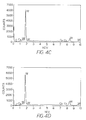
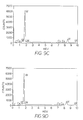
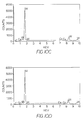
- Table I sets out,the ratio (Co/W) cobalt peak height (Co-K-alpha) and tungsten peak height (W-L-alpha) at the surface of these substrates wherein the values were taken at an edge location near the nose of the substrate and at another location in the center of the rake surface of the substrate.
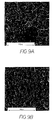
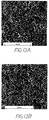
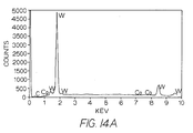
- Table I also presents the surface roughness in microinches, R a , for the rake surface. For each one of the samples, Table I also matches up the photomicrographs (FIGS. 3A-14) and the EDS spectra (FIGS 3C through 14A).
- FIG. 4C & 4D 0.02/0.02 68.32 Comparative/Re-sinter at 2800 °F for 3 hrs.
- FIGS. 5C & 5D 0.02/0.08 63.22 FIG. 5A & 5B Inventive/ Re-sinter at 2800 °F for 3 hrs.
- Electro Dip [1 amp for 30 seconds] FIGS. 6C & 6D 0.01/0.04 53.85
- FIG. 6A & 6B Comparative/ Re-sinter at 2800 °F for 3 hrs.
- FIGS. 7C & 7D 0.04/0.08 62.56 FIG. 7A & 7B Inventive/ Re-sinter at 2800 °F for 3 hrs.
- FIGS. 8C & 8D 0.01/0.03 59.02
- FIG, 8A & 8B Comparative/ Re-sinter at 2800 °F for 4 hrs
- FIGS. 9C & 9D 0.01/0.06 73.79
- FIG. 9A & 9B Inventive/ Re-sinter at 2800 °F for 4 hrs.
- Electro Dip [1amp for 30 seconds]
- FIG. 10A & 10B Comparative/Re-sinter at 2800 °F for 4 hrs.
- FIGS. 11C & 11D 0.17/0.20 63.98 FIG.
- FIGS. 12C & 12D Comparative/ Re-sinter at 2800 °F for 4 hrs.
- FIG. 13A & 13B Inventive/ Re-sinter at 2800 °F for 4 hrs. & Electro Dip [1 amp for 30 seconds]
- Table II sets forth the averages of the information presented in Table I above for the samples that were subjected to the re-sintering for 3 hours. Average Values for Co/W Peak Ratio and Rake Surface Roughness Of Samples Re-Sintered at 2800 °F (1538 °C) for 3 Hours Sample Co/W Peak Ratio Edge Adjacent Nose Co/W Peak Ratio Center of Rake Surface Surface Roughness Microinches, R a of Rake Surface Comparative [Re-Sintered Substrate] .030 .077 61.1 Inventive [Treated substrate] .013 .030 60.4
- Table III sets forth the averages of the information presented in Table I above for the samples that were subjected to the re-sintering for 4 hours. Average Values for Co/W Peak Ratio and Rake Surface Roughness Of Samples Re-Sintered at 2800 °F (1538 °C) for 4 Hours Sample Co/W Peak Ratio Edge Adjacent Nose Co/W Peak Ratio Center of Rake Surface Surface Roughness Microinches, R a of Rake Surface Comparative [Re-Sintered Substrate] .07 .11 64.3 Inventive [Treated Substrate] .01 .01 59.0
- the Co/W Peak Ratios are reduced through the present invention.
- the average value of the Co/W Peak Ratio at the edge adjacent the nose was reduced from .07 to .01 through the use of the present invention.
- the average value of the Co/W Peak Ratio at the center of the rake surface was reduced from .11 to .01 through the use of the present invention.
- a sintered substrate [K203T] (Sample ASV 556) that had a composition of 0.02-0.03 weight percent tantalum; less than 0.01 weight percent of the following elements: titanium, niobium, nickel, vanadium, chromium, molybdenum, and hafnium; .13 weight percent iron, 6.04-6.09 weight percent cobalt; and the balance was tungsten and carbon wherein most of the tungsten and carbon was in the form of tungsten carbide.
- the magnetic saturation value was 17.82 microtesla cubic meter per kilogram cobalt.
- the hardness of the sintered substrate in the bulk region thereof was 89.4 Rockwell A.
- the grain size of the tungsten carbide in the bulk region was between about 3 micrometers and about 13 micrometers.
- the porosity of the sintered substrate determined according to ASTM Designation B276-91 (Reapproved 1996) was A02+B00+C00 at the edges and A02+B00.2+C00. There was no eta phase present in the re-sintered substrate.
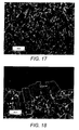
- FIG.15 is a photomicrograph that shows the microstructure of the bulk region of the sintered substrate of this sample (ASV556) after a two minute etching treatment.
- the microstructure is typical except for a few larger size grains of tungsten carbide.
- the substrate was sintered by itself (i.e., no materials of differing composition were included) at a temperature of about 2700 degrees Fahrenheit (about 1482 degrees Centigrade) for a duration of 45 minutes.
- the average tungsten carbide grain size of the surface region was 22.2 micrometers and the average tungsten carbide grain size of the bulk region was 11.7 micrometers.
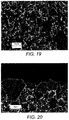
- Fig.19 shows the microstructure of the bulk region of the second one of examples (ASW 455).
- Fig. 20 shows the microstructure of the surface region of the second one of the examples (ASW 455).
- a sintered substrate (Sample ASV 555) that had a composition of: 0.01-0.02 weight percent tantalum; less than 0.01 weight percent of the following elements: titanium, niobium, nickel, vanadium, chromium, molybdenum, and hafnium; 0.13-0.14 weight percent iron; 5.94-5.989 weight percent cobalt; and the balance being tungsten and carbon with most of the tungsten and carbon being in the form of tungsten carbide.
- the magnetic saturation value was 17.96 microtesla cubic meter per kilogram cobalt.
- the hardness of the bulk region of the sintered substrate was 89.5 Rockwell A.
- the average tungsten carbide grain size in the bulk region was between about 3 micrometers and about 13 micrometers.
- the porosity of the sintered substrate determined according to ASTM Designation B276-91 (Reapproved 1996) was A02+B00-1+C00. There was no eta phase present in the sintered substrate.
- FIG.16 is a photomicrograph that shows the typical microstructure of the bulk region of the sintered substrate of this sample after a two minute etching treatment. Referring to FIG. 16, the microstructure present therein has a generally uniform appearance.
- the substrate was co-sintered along with other material at a temperature of about 2700 degrees Fahrenheit (about 1482 degrees Centigrade) for a duration of 45 minutes.
- the material with which the substrate was co-sintered did not contain a substantial amount of grain growth inhibitors (e.g., vanadium, chromium, tantalum, titanium, niobium).
- FIG. 22 shows the microstructure of the surface region of the first one of the examples (ASW 456).
- the surface region had an average grain size of 28.7 micrometers and the bulk region had an average grain size of 10.3 micrometers.
- FIG.23 shows the microstructure of the bulk region of the second one of the examples (ASW 457).
- FIG.24 shows the microstructure of the surface region of the second one of the examples (ASW 457).
- a sintered substrate (Sample ASV 557) that had a composition of: 0.02 weight percent tantalum; 0.13-0.14 weight percent iron; less than 0.01 weight percent of the following elements: titanium, niobium, nickel, vanadium, chromium, molybdenum, and hafnium; 6.06-6.085 weight percent cobalt; and the balance tungsten and carbon wherein most of the tungsten and carbon is in the form of tungsten carbide.
- the substrate was sintered by itself at a temperature of about 2625 degrees Fahrenheit (about 1441 degrees Centigrade) for a duration of 45 minutes.
- the magnetic saturation value was between 18.2 and 20.2 microtesla cubic meter per kilogram cobalt.
- FIG. 25 shows the typical microstructure of the sintered substrate.
- the hardness of the sintered substrate was 89.6 Rockwell A.
- the average grain size of the tungsten carbide in the bulk region was between about 3 micrometers and about 13 micrometers included with a few larger grains of tungsten carbide to a size of 19 micrometers and a patch of fine-grained cemented (cobalt) tungsten carbide.
- the porosity of the sintered substrate determined according to ASTM Designation B276-91 (Reapproved 1996) was A02+B00+C00 at the edges and A02+B00+C00. There was no eta phase present in the sintered substrate.
- the surface region had an average grain size of 28.4 micrometers and the bulk region had an average grain size of 8.9 micrometers.
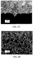
- FIG. 28 shows the microstructure of the bulk region of the second one of the examples (ASW 459).
- FIG. 29 shows the microstructure of the surface region of the second one of the examples (ASW 459).
- a sintered substrate (ASW073) that had a composition of: 0.01 weight percent tantalum; 0.13-0.14 weight percent iron; less than 0.01 weight percent of the following elements: titanium, niobium, nickel, vanadium, chromium, molybdenum and hafnium; 6.05-6.06 weight percent cobalt; and the balance tungsten and carbon with most of the tungsten and carbon being in the form of tungsten carbide.
- FIG. 30 shows the typical microstructure of the bulk region of this sample after a two minute etching treatment.
- the hardness of the sintered substrate was 89.2 Rockwell A.
- the average grain size of the tungsten carbide grains in the bulk region was between about 3 micrometers and about 13 micrometers.
- the porosity of the re-sintered substrate determined according to ASTM Designation B276-91 (Reapproved 1996) was A04+B04+C00.
- the surface region had an average grain size for the tungsten carbide of 55.1 micrometers and the bulk region had an average grain size of 9.0 micrometers.
- FIG. 31 shows the microstructure of the bulk region of the first example (ASW 460).
- FIG. 32 shows the microstructure of the surface region of the first example (ASW 460).
- the surface region had an average grain size for the tungsten carbide of 29.7 micrometers and the bulk region had an average grain size for the tungsten carbide of 10.2 micrometers.
- FIG. 33 shows the microstructure of the bulk region of the second example (ASW 461).
- FIG. 34 shows the microstructure of the surface region of the second example (ASW 461).
Landscapes
- Chemical & Material Sciences (AREA)
- Materials Engineering (AREA)
- Mechanical Engineering (AREA)
- Engineering & Computer Science (AREA)
- Metallurgy (AREA)
- Chemical Kinetics & Catalysis (AREA)
- General Chemical & Material Sciences (AREA)
- Organic Chemistry (AREA)
- Inorganic Chemistry (AREA)
- Composite Materials (AREA)
- Manufacturing & Machinery (AREA)
- Cutting Tools, Boring Holders, And Turrets (AREA)
- Chemical Vapour Deposition (AREA)
- Polishing Bodies And Polishing Tools (AREA)
- Powder Metallurgy (AREA)
Abstract
Description
| Cobalt/Tungsten Ratio and Surface Roughness For Comparative Samples and Inventive Samples | ||||
| Sample & Processing | EDS Spectrum | Co/W Peak Ratio at Edge adjacent Nose / Center of Rake Surface | Surface Roughness Microinches, Ra /Rake Surface | Photomicrographs (Edge adjacent Nose & Center of Rake Surface) |
| Comparative/ Resinter at 2800 °F for 3 hrs | FIGS. 3C & 3D | 0.03/0.07 | 57.68 | FIG. 3A & FIG. 3B |
| Inventive/ Re-sinter at 2800 °F for 3 hrs. & Electro Dip [1 amp for 30 seconds] | FIGS. 4C & 4D | 0.02/0.02 | 68.32 | FIG, 4A & 4B |
| Comparative/Re-sinter at 2800 °F for 3 hrs. | FIGS. 5C & 5D | 0.02/0.08 | 63.22 | FIG. 5A & 5B |
| Inventive/ Re-sinter at 2800 °F for 3 hrs. & Electro Dip [1 amp for 30 seconds] | FIGS. 6C & 6D | 0.01/0.04 | 53.85 | FIG. 6A & 6B |
| Comparative/ Re-sinter at 2800 °F for 3 hrs. | FIGS. 7C & 7D | 0.04/0.08 | 62.56 | FIG. 7A & 7B |
| Inventive/ Re-sinter at 2800 °F for 3 hrs. & Electro Dip [1amp for 30 seconds] | FIGS. 8C & 8D | 0.01/0.03 | 59.02 | FIG, 8A & 8B |
| Comparative/ Re-sinter at 2800 °F for 4 hrs | FIGS. 9C & 9D | 0.01/0.06 | 73.79 | FIG. 9A & 9B |
| Inventive/ Re-sinter at 2800 °F for 4 hrs. & Electro Dip [1amp for 30 seconds] | FIGS. 10C & 10D | 0.01/0 | 57.11 | FIG. 10A & 10B |
| Comparative/Re-sinter at 2800 °F for 4 hrs. | FIGS. 11C & 11D | 0.17/0.20 | 63.98 | FIG. 11A & 11B |
| Inventive/ Re-sinter at 2800 °F for 4 hrs. & Electro Dip [1amp for 30 seconds] | FIGS. 12C & 12D | 0.01/0.03 | 63.94 | FIG. 12A & 12B |
| Comparative/ Re-sinter at 2800 °F for 4 hrs. | FIGS. 13C & 13D | 0.03/0.08 | 55.03 | FIG. 13A & 13B |
| Inventive/ Re-sinter at 2800 °F for 4 hrs. & Electro Dip [1 amp for 30 seconds] | FIG. 14A | 0.01/0 | 56.14 | FIG. 14 |
| Average Values for Co/W Peak Ratio and Rake Surface Roughness Of Samples Re-Sintered at 2800 °F (1538 °C) for 3 Hours | |||
| Sample | Co/W Peak Ratio Edge Adjacent Nose | Co/W Peak Ratio Center of Rake Surface | Surface Roughness Microinches, Ra of Rake Surface |
| Comparative [Re-Sintered Substrate] | .030 | .077 | 61.1 |
| Inventive [Treated substrate] | .013 | .030 | 60.4 |
| Average Values for Co/W Peak Ratio and Rake Surface Roughness Of Samples Re-Sintered at 2800 °F (1538 °C) for 4 Hours | |||
| Sample | Co/W Peak Ratio Edge Adjacent Nose | Co/W Peak Ratio Center of Rake Surface | Surface Roughness Microinches, Ra of Rake Surface |
| Comparative [Re-Sintered Substrate] | .07 | .11 | 64.3 |
| Inventive [Treated Substrate] | .01 | .01 | 59.0 |
Claims (38)
- A process for making a diamond coated cutting tool, the process comprising the following steps:providing a sintered substrate, the sintered substrate comprising tungsten carbide and cobalt, the sintered substrate having an average tungsten carbide grain size of between about 3 micrometers and about 20 micrometers;re-sintering the sintered substrate to produce a re-sintered substrate, the re-sintered substrate having a surface, and the re-sintered substrate having a surface region beginning at and extending inwardly from the surface, the re-sintered substrate having a bulk region inwardly of the surface region, and the surface region of the re-sintered substrate having an average tungsten carbide grain size of between about 12 micrometers and about 60 micrometers, the bulk region of the re-sintered substrate having an average tungsten carbide grain size of between about 3 micrometers and about 20 micrometers, and wherein the average tungsten carbide grain size in the surface region is greater than the average tungsten carbide grain size in the bulk region;subjecting the re-sintered substrate to a chemical treatment for the removal of cobalt at the surface of the re-sintered substrate to produce a treated substrate, and wherein the treated substrate has a surface with a cobalt peak/tungsten peak ratio of less than 0.2 and there being an absence of continuous porosity below the surface of the treated substrate; andadherently depositing a diamond coating to at least a portion of the surface of the treated substrate.
- The process according to claim 1 further including after completion of the chemical treatment step and before the diamond depositing step, a step of mechanically seeding/scratching the treated substrate.
- The process according to claim 1 wherein the re-sintering step occurs at a temperature of between about 1427 degrees Centigrade and about 1593 degrees Centigrade for a duration of between about 3 hours and about 7 hours and at a pressure of between about 0.5 torr and about 3 torr of nitrogen.
- The process according to claim 1 wherein the treated substrate having a surface roughness, Ra, of greater than or equal to about 25 microinches.
- The process according to claim 4 wherein the treated substrate having a surface roughness, Ra, of between about 38 microinches and about 90 microinches.
- The process according to claim 1 wherein the sintered substrate having an average tungsten carbide grain size of between about 15 micrometers and about 20 micrometers.
- The process according to claim 1 wherein the re-sintered substrate having a first level of residual surface cobalt and the treated substrate having a second level of residual surface cobalt, and the second level of residual surface cobalt being less than the first level of residual surface cobalt.
- The process according to claim 1 wherein the re-sintered substrate having a first level of residual surface cobalt and the treated substrate having a second level of residual surface cobalt, and the second level of residual surface cobalt being as low as one-tenth of the first level of residual surface cobalt.
- the process according to claim 1 wherein the sintered substrate comprising at least about 85 weight percent tungsten carbide and between about 2 weight percent and about 12 weight percent cobalt.
- The process according to claim 1 wherein the average tungsten carbide grain size in the surface region is between about 170 percent and about 620 percent greater than the average tungsten carbide grain size in the bulk region.
- The process according to claim 1 wherein the average tungsten carbide grain size in the surface region is about 170 percent and about 320 percent greater than the average tungsten carbide grain size in the bulk region.
- The process according to claim 1 wherein the average tungsten carbide grain size in the surface region is between about 170 percent and about 200 percent greater than the average tungsten carbide grain size in the bulk region.
- The process according to claim 1 wherein the average tungsten carbide grain size in the surface region is between about 180 percent and about 190 percent greater than the average tungsten carbide grain size in the bulk region.
- The process according to claim 1 wherein the magnetic saturation value of the sintered substrate being between about 17.3 and about 18.8 microtesla cubic meter per kilogram cobalt.
- The process according to claim 1 wherein the magnetic saturation value of the sintered substrate being between about 17.8 and about 18.8 microtesla cubic meter per kilogram cobalt.
- The process according to claim 1 wherein the treating step comprising dipping the re-sintered substrate in a solution with an electric current passing therethrough.
- The process according to claim 16 wherein the solution comprising about 50 volume percent sulfuric acid and about 50 volume percent phosphoric acid.
- The process according to claim 1 wherein the average tungsten carbide grain size in the surface region is between about 12 micrometers and about 30 micrometers, and the average tungsten carbide grain size in the bulk region is between about 6 micrometers and about 13 micrometers.
- The process according to claim 1 wherein the average tungsten carbide grain size in the surface region is between about 20 micrometers and about 30 micrometers, and the average tungsten carbide grain size in the bulk region is between about 6 micrometers and about 13 micrometers.
- A diamond coated cutting tool produced by a process comprising the steps of:providing a sintered substrate, the sintered substrate comprising tungsten carbide and cobalt, the sintered substrate having an average tungsten carbide grain size of between about 3 micrometers and about 20 micrometers;re-sintering the sintered substrate to produce a re-sintered substrate, the re-sintered substrate having a surface and the re-sintered substrate having a surface region beginning at and extending inwardly from the surface, the re-sintered substrate having a bulk region inwardly of the surface region, and the surface region of the re-sintered substrate having an average tungsten carbide grain size of between about 12 micrometers and about 60 micrometers, the bulk region of the re-sintered substrate having an average tungsten carbide grain size of between about 3 micrometers and about 20 micrometers, and wherein the average tungsten carbide grain size in the surface region is greater than the average tungsten carbide grain size in the bulk region; andadherently depositing a diamond coating to at least a portion of the surface of the treated substrate.
- The cutting tool according to claim 20 wherein the magnetic saturation value of the sintered substrate being between about 17.3 and about 18.8 microtesla cubic meter per kilogram cobalt.
- The cutting tool according to claim 20 wherein the magnetic saturation value of the sintered substrate being between about 17.8 and about 18.8 microtesla cubic meter per kilogram cobalt.
- The cutting tool according to claim 20 wherein the sintered substrate having an average tungsten carbide grain size of between about 15 micrometers and about 20 micrometers.
- The cutting tool according to claim 20 wherein the re-sintered substrate having a first level of residual surface cobalt and the treated substrate having a second level of residual surface cobalt, and the second level of residual surface cobalt being less than the first level of residual surface cobalt
- The cutting tool according to claim 20 wherein the re-sintered substrate having a first level of residual surface cobalt and the treated substrate having a second level of residual surface cobalt, and the second level of residual surface cobalt being as low as one-tenth of the first level of residual surface cobalt.
- The cutting tool according to claim 20 wherein the average tungsten carbide grain size in the surface region is between about 170 percent and about 320 percent greater than the average tungsten carbide grain size in the bulk region.
- The cutting tool according to claim 20 wherein the average tungsten carbide grain size in the surface region is between about 170 percent and about 200 percent greater than the average tungsten carbide grain size in the bulk region.
- The cutting tool according to claim 20 wherein the average tungsten carbide grain size in the surface region is between about 180 percent and about 190 percent greater than the average tungsten carbide grain size in the bulk region.
- A diamond coated cutting tool comprising:a re-sintered substrate, the re-sintered substrate having a composition comprising between about 2 weight percent to about 12 weight percent cobalt, and tungsten and carbon wherein most of the tungsten and carbon is in the form of tungsten carbide;the re-sintered substrate having a surface, and the surface being subjected to a chemical treatment;the re-sintered substrate having a surface region extending inwardly from the surface and a bulk region being inwardly of the surface region;the surface region having an average tungsten carbide grain size of between about 12 micrometers and about 60 micrometers;the bulk region having an average tungsten carbide grain size of between about 3 micrometers and about 20 micrometers, and wherein the average tungsten carbide grain size in the surface region is greater than the average tungsten carbide grain size in the bulk region; anda diamond coating on the surface of the re-sintered substrate.
- The diamond coated cutting tool according to claim 29 wherein the average tungsten carbide grain size in the surface region is between about 170 percent and about 320 percent greater than the average tungsten carbide grain size in the bulk region.
- The diamond coated cutting tool according to claim 29 wherein the average tungsten carbide grain size in the surface region is between about 170 percent and about 200 percent greater than the average tungsten carbide grain size in the bulk region.
- The diamond coated cutting tool according to claim 29 wherein the average tungsten carbide grain size in the surface region is between about 170 percent to about 190 percent greater than the average tungsten carbide grain size in the bulk region.
- A diamond coated cutting tool comprising:a re-sintered substrate, the re-sintered substrate having a composition comprising between about 2 weight percent to about 12 weight percent cobalt, and tungsten and carbon wherein most of the tungsten and carbon is in the form of tungsten carbide;the re-sintered substrate having a surface, and the surface being subjected to a chemical treatment;the re-sintered substrate having a surface region extending inwardly from the surface and a bulk region being inwardly of the surface region;the bulk region having an average tungsten carbide grain size of between about 3 micrometers and about 20, and wherein the average tungsten carbide grain size in the surface region is greater than the average tungsten carbide grain size in the bulk region; anda diamond coating on the surface of the re-sintered substrate.
- The diamond coated cutting tool according to claim 33 wherein the average tungsten carbide grain size in the surface region is between about 170 percent and about 320 percent greater than the average tungsten carbide grain size in the bulk region.
- The diamond coated cutting tool according to claim 33 wherein the average tungsten carbide grain size in the surface region is about 170 percent and about 200 percent greater than the average tungsten carbide grain size in the bulk region.
- The diamond coated cutting tool according to claim 33 wherein the average tungsten carbide grain size in the surface region is about between 180 percent and about 190 percent greater than the average tungsten carbide grain size in the bulk region.
- The diamond coated cutting tool according to claim 33 wherein the surface region having an average tungsten carbide grain size of between about 12 micrometers and about 30 micrometers.
- The diamond coated cutting tool according to claim 33 wherein the surface region having an average tungsten carbide grain size of between about 20 micrometers and about 30 micrometers.
Applications Claiming Priority (2)
| Application Number | Priority Date | Filing Date | Title |
|---|---|---|---|
| US946545 | 2001-09-05 | ||
| US09/946,545 US6660329B2 (en) | 2001-09-05 | 2001-09-05 | Method for making diamond coated cutting tool |
Publications (2)
| Publication Number | Publication Date |
|---|---|
| EP1291450A2 true EP1291450A2 (en) | 2003-03-12 |
| EP1291450A3 EP1291450A3 (en) | 2004-04-14 |
Family
ID=25484628
Family Applications (1)
| Application Number | Title | Priority Date | Filing Date |
|---|---|---|---|
| EP02019797A Withdrawn EP1291450A3 (en) | 2001-09-05 | 2002-09-05 | Diamond coated cutting tool and method for making the same |
Country Status (5)
| Country | Link |
|---|---|
| US (2) | US6660329B2 (en) |
| EP (1) | EP1291450A3 (en) |
| CA (1) | CA2401305A1 (en) |
| DE (1) | DE1291450T1 (en) |
| ES (1) | ES2193898T1 (en) |
Cited By (1)
| Publication number | Priority date | Publication date | Assignee | Title |
|---|---|---|---|---|
| WO2011135100A1 (en) | 2010-04-30 | 2011-11-03 | Cemecon Ag | Coated body and a process for coating a body |
Families Citing this family (9)
| Publication number | Priority date | Publication date | Assignee | Title |
|---|---|---|---|---|
| US7017677B2 (en) * | 2002-07-24 | 2006-03-28 | Smith International, Inc. | Coarse carbide substrate cutting elements and method of forming the same |
| US7407525B2 (en) * | 2001-12-14 | 2008-08-05 | Smith International, Inc. | Fracture and wear resistant compounds and down hole cutting tools |
| US6998211B2 (en) * | 2002-05-16 | 2006-02-14 | Troy Group, Inc. | System for producing secure toner-based images and methods of forming and using the same |
| AU2003277912A1 (en) * | 2002-09-27 | 2004-04-23 | Cemecon Ag | Coating method and coated element |
| JP4313587B2 (en) * | 2003-03-03 | 2009-08-12 | 株式会社タンガロイ | Cemented carbide and coated cemented carbide members and methods for producing them |
| US20050262774A1 (en) * | 2004-04-23 | 2005-12-01 | Eyre Ronald K | Low cobalt carbide polycrystalline diamond compacts, methods for forming the same, and bit bodies incorporating the same |
| US8202335B2 (en) | 2006-10-10 | 2012-06-19 | Us Synthetic Corporation | Superabrasive elements, methods of manufacturing, and drill bits including same |
| SE0701449L (en) * | 2007-06-01 | 2008-12-02 | Sandvik Intellectual Property | Fine-grained cemented carbide with refined structure |
| WO2013002270A1 (en) * | 2011-06-27 | 2013-01-03 | 京セラ株式会社 | Hard alloy and cutting tool |
Family Cites Families (43)
| Publication number | Priority date | Publication date | Assignee | Title |
|---|---|---|---|---|
| US4348263A (en) | 1980-09-12 | 1982-09-07 | Western Electric Company, Inc. | Surface melting of a substrate prior to plating |
| US4414244A (en) | 1982-06-16 | 1983-11-08 | The United States Of America As Represented By The United States Department Of Energy | Surface modification to waveguides |
| JPS6086096A (en) | 1983-10-18 | 1985-05-15 | Natl Inst For Res In Inorg Mater | Membrane diamond precipitation method |
| JPS60107000A (en) | 1983-11-16 | 1985-06-12 | Citizen Watch Co Ltd | Method for finishing surface of accessory to provide satin surface |
| JPS6152363A (en) | 1984-08-21 | 1986-03-15 | Mitsubishi Metal Corp | Method for depositing and forming artificial diamond film on surface of cermet member |
| JPH0672302B2 (en) | 1985-09-19 | 1994-09-14 | 住友電気工業株式会社 | Manufacturing method of hard carbon film coated cemented carbide |
| US4851254A (en) | 1987-01-13 | 1989-07-25 | Nippon Soken, Inc. | Method and device for forming diamond film |
| JPS63199870A (en) | 1987-02-16 | 1988-08-18 | Showa Denko Kk | Diamond coated sintered hard tool material |
| JPS63210099A (en) | 1987-02-26 | 1988-08-31 | Nissin Electric Co Ltd | Preparation of diamond film |
| JP2587431B2 (en) | 1987-10-30 | 1997-03-05 | 三菱重工業株式会社 | Manufacturing method of diamond coated member |
| JP2597497B2 (en) | 1988-01-14 | 1997-04-09 | 洋一 広瀬 | Synthesis method of vapor phase diamond |
| JPH01201475A (en) | 1988-02-08 | 1989-08-14 | Hitachi Ltd | Production of tool coated with thin diamond film |
| EP0374923B2 (en) | 1988-12-21 | 1999-06-23 | Mitsubishi Materials Corporation | Diamond-coated tool member, substrate thereof and method for producing same |
| US5304461A (en) | 1989-01-10 | 1994-04-19 | Kabushiki Kaisha Kobe Seiko Sho | Process for the selective deposition of thin diamond film by gas phase synthesis |
| JP2720384B2 (en) | 1989-02-17 | 1998-03-04 | 日本特殊陶業株式会社 | Coating method with diamond thin film |
| US5094878A (en) | 1989-06-21 | 1992-03-10 | Nippon Soken, Inc. | Process for forming diamond film |
| DE69018243T2 (en) | 1989-09-22 | 1995-07-27 | Showa Denko Kk | METHOD FOR PRODUCING DIAMOND BY MEANS OF VAPOR DEPOSITION ON ELECTROCHEMICALLY TREATED SUBSTRATE. |
| SE9101469D0 (en) | 1991-05-15 | 1991-05-15 | Sandvik Ab | ETSMETOD |
| US5176803A (en) | 1992-03-04 | 1993-01-05 | General Electric Company | Method for making smooth substrate mandrels |
| US5268045A (en) | 1992-05-29 | 1993-12-07 | John F. Wolpert | Method for providing metallurgically bonded thermally sprayed coatings |
| US5474021A (en) | 1992-09-24 | 1995-12-12 | Sumitomo Electric Industries, Ltd. | Epitaxial growth of diamond from vapor phase |
| JPH06152363A (en) | 1992-11-13 | 1994-05-31 | Yaskawa Electric Corp | Gate drive circuit |
| US5585176A (en) * | 1993-11-30 | 1996-12-17 | Kennametal Inc. | Diamond coated tools and wear parts |
| DE69503285T2 (en) | 1994-04-07 | 1998-11-05 | Sumitomo Electric Industries | Diamond wafer and method for manufacturing a diamond wafer |
| US6063149A (en) | 1995-02-24 | 2000-05-16 | Zimmer; Jerry W. | Graded grain size diamond layer |
| US5891522A (en) * | 1995-05-24 | 1999-04-06 | Saint-Gobain Industrial Ceramics, Inc. | Composite article with adherent CVD diamond coating and method of making |
| US5722803A (en) * | 1995-07-14 | 1998-03-03 | Kennametal Inc. | Cutting tool and method of making the cutting tool |
| US5650059A (en) | 1995-08-11 | 1997-07-22 | Credo Tool Company | Method of making cemented carbide substrate |
| US5759623A (en) | 1995-09-14 | 1998-06-02 | Universite De Montreal | Method for producing a high adhesion thin film of diamond on a Fe-based substrate |
| US5961718A (en) | 1995-10-16 | 1999-10-05 | National Science Council | Process for selectively depositing diamond films |
| US5858539A (en) | 1995-12-22 | 1999-01-12 | Sandvik Ab | Diamond coated body and method of its production |
| EP0824605B1 (en) | 1995-12-22 | 2002-07-17 | Sandvik Aktiebolag (publ) | Diamond coated body and method of its production |
| US5952102A (en) | 1996-05-13 | 1999-09-14 | Ceramatec, Inc. | Diamond coated WC and WC-based composites with high apparent toughness |
| US5716170A (en) * | 1996-05-15 | 1998-02-10 | Kennametal Inc. | Diamond coated cutting member and method of making the same |
| JPH10310494A (en) | 1996-05-31 | 1998-11-24 | Ngk Spark Plug Co Ltd | Method for manufacturing superhard member with diamond coating film |
| US5976707A (en) | 1996-09-26 | 1999-11-02 | Kennametal Inc. | Cutting insert and method of making the same |
| JPH10138027A (en) | 1996-11-11 | 1998-05-26 | Shinko Kobelco Tool Kk | Cemented carbide for drill and drill for printed board drilling using same cemented carbide |
| US5701578A (en) * | 1996-11-20 | 1997-12-23 | Kennametal Inc. | Method for making a diamond-coated member |
| US6022175A (en) | 1997-08-27 | 2000-02-08 | Kennametal Inc. | Elongate rotary tool comprising a cermet having a Co-Ni-Fe binder |
| DE19757242A1 (en) | 1997-12-22 | 1999-07-01 | Beck August Gmbh Co | Drilling tool for drilling in solid material |
| US6267867B1 (en) * | 1998-05-26 | 2001-07-31 | Saint-Gobain Industrial Ceramics, Inc. | Composite article with adherent CVD diamond coating and method of making |
| JP2000326105A (en) * | 1999-05-13 | 2000-11-28 | Mitsubishi Materials Corp | Surface coated cemented carbide cutting tool with artificial diamond coating layer with excellent adhesion |
| US6638474B2 (en) * | 2000-03-24 | 2003-10-28 | Kennametal Inc. | method of making cemented carbide tool |
-
2001
- 2001-09-05 US US09/946,545 patent/US6660329B2/en not_active Expired - Fee Related
-
2002
- 2002-09-04 CA CA002401305A patent/CA2401305A1/en not_active Abandoned
- 2002-09-05 DE DE1291450T patent/DE1291450T1/en active Pending
- 2002-09-05 ES ES02019797T patent/ES2193898T1/en active Pending
- 2002-09-05 EP EP02019797A patent/EP1291450A3/en not_active Withdrawn
-
2003
- 2003-08-06 US US10/635,832 patent/US6890655B2/en not_active Expired - Fee Related
Cited By (2)
| Publication number | Priority date | Publication date | Assignee | Title |
|---|---|---|---|---|
| WO2011135100A1 (en) | 2010-04-30 | 2011-11-03 | Cemecon Ag | Coated body and a process for coating a body |
| US9175384B2 (en) | 2010-04-30 | 2015-11-03 | Cemecon Ag | Coated body and a process for coating a body |
Also Published As
| Publication number | Publication date |
|---|---|
| US6660329B2 (en) | 2003-12-09 |
| ES2193898T1 (en) | 2003-11-16 |
| CA2401305A1 (en) | 2003-03-05 |
| DE1291450T1 (en) | 2003-09-18 |
| US6890655B2 (en) | 2005-05-10 |
| US20040028892A1 (en) | 2004-02-12 |
| EP1291450A3 (en) | 2004-04-14 |
| US20030049434A1 (en) | 2003-03-13 |
Similar Documents
| Publication | Publication Date | Title |
|---|---|---|
| US5716170A (en) | Diamond coated cutting member and method of making the same | |
| US5068148A (en) | Diamond-coated tool member, substrate thereof and method for producing same | |
| CA2173354C (en) | Diamond-coated tools and process for making | |
| EP1309733B1 (en) | Chromium-containing cemented carbide body having a surface zone of binder enrichment | |
| EP3589768B1 (en) | Coated cutting tool | |
| EP0515340B1 (en) | Titanium based carbonitride alloy with binder phase enrichment | |
| US20040141867A1 (en) | Composite material and method for production thereof | |
| US6660329B2 (en) | Method for making diamond coated cutting tool | |
| US8192793B2 (en) | Coated cutting insert for milling applications | |
| CA2348851A1 (en) | Diamond coated cutting tools and method of manufacture | |
| EP1253124B1 (en) | Highly adhesive surface-coated cemented carbide and method for producing the same | |
| EP0627498B1 (en) | Ceramic-based substrate, and methods for producing same | |
| WO2010068168A1 (en) | Method of making cutting tool inserts with high demands on dimensional accuracy | |
| JP3469310B2 (en) | Ceramic base material for diamond coating and method for producing coating material | |
| JP2748583B2 (en) | Surface-coated tungsten carbide based cemented carbide cutting tool with excellent adhesion of hard coating layer | |
| JP3368794B2 (en) | Surface-coated cermet throw-away type cutting insert with a hard coating layer with excellent fracture resistance | |
| JPH05209274A (en) | Manufacture of diamond coated member | |
| JPH05237707A (en) | Coated tool | |
| JP3463502B2 (en) | Surface-coated cermet throw-away type cutting insert with a hard coating layer with excellent fracture resistance | |
| JPH10286702A (en) | Surface-coated cermet throw-away type cutting insert with a hard coating layer with excellent fracture resistance | |
| JPH03219078A (en) | Diamond-coated cutting tool and its production | |
| JPH10158817A (en) | Surface coated cemented carbide cutting tool with excellent chipping resistance | |
| JPH081407A (en) | Surface coated cemented carbide cutting tool | |
| JPH1180933A (en) | Surface coated cemented carbide cutting tool with excellent chipping resistance |
Legal Events
| Date | Code | Title | Description |
|---|---|---|---|
| PUAI | Public reference made under article 153(3) epc to a published international application that has entered the european phase |
Free format text: ORIGINAL CODE: 0009012 |
|
| AK | Designated contracting states |
Kind code of ref document: A2 Designated state(s): AT BE BG CH CY CZ DE DK EE ES FI FR GB GR IE IT LI LU MC NL PT SE SK TR Designated state(s): AT BE BG CH CY CZ DE DK EE ES FI FR GB GR IE IT LI LU MC NL PT SE SK TR |
|
| AX | Request for extension of the european patent |
Extension state: AL LT LV MK RO SI |
|
| REG | Reference to a national code |
Ref country code: SE Ref legal event code: TRCL |
|
| EL | Fr: translation of claims filed | ||
| DET | De: translation of patent claims | ||
| PUAL | Search report despatched |
Free format text: ORIGINAL CODE: 0009013 |
|
| AK | Designated contracting states |
Kind code of ref document: A3 Designated state(s): AT BE BG CH CY CZ DE DK EE ES FI FR GB GR IE IT LI LU MC NL PT SE SK TR |
|
| AX | Request for extension of the european patent |
Extension state: AL LT LV MK RO SI |
|
| RIC1 | Information provided on ipc code assigned before grant |
Ipc: 7C 23C 16/27 B Ipc: 7C 23C 16/02 A |
|
| 17P | Request for examination filed |
Effective date: 20040927 |
|
| AKX | Designation fees paid |
Designated state(s): AT |
|
| REG | Reference to a national code |
Ref country code: DE Ref legal event code: 8566 |
|
| 17Q | First examination report despatched |
Effective date: 20060718 |
|
| STAA | Information on the status of an ep patent application or granted ep patent |
Free format text: STATUS: THE APPLICATION IS DEEMED TO BE WITHDRAWN |
|
| 18D | Application deemed to be withdrawn |
Effective date: 20071130 |