EP1289052A2 - Antenna with an integral RF circuit, antenna module and communication apparatus incorporating the same - Google Patents
Antenna with an integral RF circuit, antenna module and communication apparatus incorporating the same Download PDFInfo
- Publication number
- EP1289052A2 EP1289052A2 EP02017815A EP02017815A EP1289052A2 EP 1289052 A2 EP1289052 A2 EP 1289052A2 EP 02017815 A EP02017815 A EP 02017815A EP 02017815 A EP02017815 A EP 02017815A EP 1289052 A2 EP1289052 A2 EP 1289052A2
- Authority
- EP
- European Patent Office
- Prior art keywords
- circuit
- disposed
- antenna
- dielectric base
- radiation electrodes
- Prior art date
- Legal status (The legal status is an assumption and is not a legal conclusion. Google has not performed a legal analysis and makes no representation as to the accuracy of the status listed.)
- Granted
Links
Images

Classifications
-
- H—ELECTRICITY
- H01—ELECTRIC ELEMENTS
- H01Q—ANTENNAS, i.e. RADIO AERIALS
- H01Q1/00—Details of, or arrangements associated with, antennas
- H01Q1/12—Supports; Mounting means
- H01Q1/22—Supports; Mounting means by structural association with other equipment or articles
- H01Q1/24—Supports; Mounting means by structural association with other equipment or articles with receiving set
- H01Q1/241—Supports; Mounting means by structural association with other equipment or articles with receiving set used in mobile communications, e.g. GSM
- H01Q1/242—Supports; Mounting means by structural association with other equipment or articles with receiving set used in mobile communications, e.g. GSM specially adapted for hand-held use
- H01Q1/243—Supports; Mounting means by structural association with other equipment or articles with receiving set used in mobile communications, e.g. GSM specially adapted for hand-held use with built-in antennas
-
- H—ELECTRICITY
- H01—ELECTRIC ELEMENTS
- H01Q—ANTENNAS, i.e. RADIO AERIALS
- H01Q1/00—Details of, or arrangements associated with, antennas
- H01Q1/36—Structural form of radiating elements, e.g. cone, spiral, umbrella; Particular materials used therewith
- H01Q1/38—Structural form of radiating elements, e.g. cone, spiral, umbrella; Particular materials used therewith formed by a conductive layer on an insulating support
-
- H—ELECTRICITY
- H01—ELECTRIC ELEMENTS
- H01Q—ANTENNAS, i.e. RADIO AERIALS
- H01Q1/00—Details of, or arrangements associated with, antennas
- H01Q1/52—Means for reducing coupling between antennas; Means for reducing coupling between an antenna and another structure
- H01Q1/521—Means for reducing coupling between antennas; Means for reducing coupling between an antenna and another structure reducing the coupling between adjacent antennas
- H01Q1/525—Means for reducing coupling between antennas; Means for reducing coupling between an antenna and another structure reducing the coupling between adjacent antennas between emitting and receiving antennas
-
- H—ELECTRICITY
- H01—ELECTRIC ELEMENTS
- H01Q—ANTENNAS, i.e. RADIO AERIALS
- H01Q23/00—Antennas with active circuits or circuit elements integrated within them or attached to them
-
- H—ELECTRICITY
- H01—ELECTRIC ELEMENTS
- H01Q—ANTENNAS, i.e. RADIO AERIALS
- H01Q9/00—Electrically-short antennas having dimensions not more than twice the operating wavelength and consisting of conductive active radiating elements
- H01Q9/04—Resonant antennas
- H01Q9/0407—Substantially flat resonant element parallel to ground plane, e.g. patch antenna
-
- H—ELECTRICITY
- H05—ELECTRIC TECHNIQUES NOT OTHERWISE PROVIDED FOR
- H05K—PRINTED CIRCUITS; CASINGS OR CONSTRUCTIONAL DETAILS OF ELECTRIC APPARATUS; MANUFACTURE OF ASSEMBLAGES OF ELECTRICAL COMPONENTS
- H05K1/00—Printed circuits
- H05K1/02—Details
- H05K1/0213—Electrical arrangements not otherwise provided for
- H05K1/0237—High frequency adaptations
-
- H—ELECTRICITY
- H05—ELECTRIC TECHNIQUES NOT OTHERWISE PROVIDED FOR
- H05K—PRINTED CIRCUITS; CASINGS OR CONSTRUCTIONAL DETAILS OF ELECTRIC APPARATUS; MANUFACTURE OF ASSEMBLAGES OF ELECTRICAL COMPONENTS
- H05K1/00—Printed circuits
- H05K1/02—Details
- H05K1/14—Structural association of two or more printed circuits
- H05K1/141—One or more single auxiliary printed circuits mounted on a main printed circuit, e.g. modules, adapters
Definitions
- the present invention relates to an antenna with an integral RF circuit that can be mounted on a circuit board of a communication apparatus, an antenna module including such an antenna, and a communication apparatus including such an antenna.
- surface-mount antennas that is, chip antennas that can be mounted on a circuit board of a communication apparatus, have been actively researched and developed.
- radiation electrodes for transmitting or receiving radio waves are disposed on a dielectric base.
- a plurality of radiation electrodes is disposed on a dielectric base so that radio waves in a plurality of frequency bands can be transmitted or received by a single surface-mount antenna.
- the dielectric constant of the dielectric base which is a factor that contributes to reduction in size, strengthens coupling between the radiation electrodes.
- a large space is required between the radiation electrodes in order to ensure isolation between the radiation electrodes, leading to an increase in the size of an antenna.
- the increase in the size of the antenna prevents a reduction in the size of a communication apparatus.
- preferred embodiments of the present invention provide an antenna with an integral RF circuit that readily facilitates reduction in the size of a communication apparatus, an antenna module including such a novel antenna, and a communication apparatus including such a novel antenna.
- an antenna with an integral RF circuit includes a dielectric base, a top surface thereof being substantially flat, a plurality of radiation electrodes for one of or both transmission and reception of a radio wave, disposed on the top surface of the dielectric base and spaced from each other, an integral RF circuit having a circuit pattern and connected to at least one of the plurality of radiation electrodes conductively or via a capacitor, the FR circuit being disposed at least partially in a gap between the radiation electrodes, a concavity formed in a bottom surface of the dielectric base in a region corresponding to an area where the circuit pattern of the RF circuit is located, the concavity defining a thin portion and a thick portion in the dielectric base, the circuit pattern of the RF circuit being disposed on the thin portion of the dielectric base and the plurality of radiation electrodes being disposed on the thick portion of the dielectric base, and a ground electrode disposed on the bottom surface of the dielectric base and on an inner surface of the concav
- the plurality of radiation electrodes preferably has different resonant frequencies from each other.
- the plurality of radiation electrodes disposed on the top surface of the dielectric base preferably includes at least one radiation electrode dedicated for reception and at least one radiation electrode dedicated for transmission.
- the RF circuit is preferably provided in one-to-one association with each of the plurality of radiation electrodes.
- Another preferred embodiment of the present invention provides an antenna module including an antenna with the integral RF circuit described above, the antenna module being joined with a substrate with a bottom surface defining a connecting surface, a circuit conductively connected to the RF circuit of the antenna with the integral RF circuit and disposed in an area on the substrate surrounded by the concavity on the bottom surface of the antenna with the integral RF circuit, and a connecting device for conductively connecting the circuit and the RF circuit.
- the connecting device may include a through hole formed in the dielectric base of the antenna with the integral RF circuit.
- the connecting device may include a wiring pattern disposed on a side surface of the dielectric base of the antenna with an integral RF circuit.
- the connecting device may include a metallic pin disposed so as to penetrate through the dielectric base of the antenna with an integral RF circuit from the top surface to the bottom surface.
- a communication apparatus includes an antenna with the integral RF circuit described above or an antenna module described above.
- a plurality of radiation electrodes are spaced from each other on a top surface of a dielectric base, and an integral RF circuit is arranged so as to be disposed at least partially in a gap between the radiation electrodes. Because the RF circuit is thus arranged on the dielectric base to efficiently utilize the gap between the plurality of radiation electrodes, any increase in the size of the dielectric base is prevented, and the RF circuit and the plurality of radiation electrodes can be disposed on the dielectric base.
- the RF circuit is disposed in the antenna, the RF circuit need not be disposed on a circuit board of a communication apparatus, allowing the circuit board to be made much smaller which allows for significant reduction in the size of the communication apparatus.
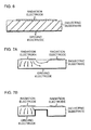
- the radiation electrodes resonate favorably, so that performance of transmission or reception of radio waves is greatly improved. Furthermore, by disposing a circuit pattern on a thin portion of the dielectric base, an electric field of the circuit pattern is confined, thereby greatly reducing radiation loss attributed to radiation of radio waves from the circuit pattern. Furthermore, compared with a case where a plurality of radiation electrodes is disposed on a uniformly thick dielectric base as shown in Fig. 7A, by making a portion of the dielectric base between the radiation electrodes thin with a concavity as shown in Fig. 7B, coupling between the radiation electrodes is diminished. Furthermore, another circuit can be disposed and included within the concavity.
- a plurality of radiation electrodes are arranged so as to be spaced from each other on a substantially flat top surface of a dielectric base, and an integral RF circuit is arranged at least partially in a gap between the radiation electrodes. Accordingly, the radiation electrodes are separated from each other by such a space where the RF circuit is located, so that isolation between the radiation electrodes is ensured. Furthermore, a portion of the dielectric base between the radiation electrodes is made thin because of the formation of the concavity, so that coupling between the radiation electrodes is minimized. This also contributes to ensure isolation between the radiation electrodes.
- the gap between the radiation electrodes is efficiently used to provide an integral RF circuit. Accordingly, even if an integral RF circuit is disposed on a dielectric base, an increase in the size of the dielectric base is prevented thereby preventing any increase in cost.
- an integral RF circuit is disposed on a dielectric base of an antenna, the RF circuit need not be provided on a circuit board of a communication apparatus, allowing the circuit board to be made smaller, thereby facilitating reduction in the size of the communication apparatus.
- radiation electrodes and RF circuits are disposed on the same surface and disposed in proximity to each other, conduction paths for signals between the radiation electrodes and the RF circuits are extremely short, thereby significantly reducing conduction loss.
- the radiation electrodes because radiation electrodes are disposed on a thick portion of a dielectric base, the radiation electrodes favorably transmit or receive radio waves. Furthermore, because a circuit pattern of an integral RF circuit is disposed on a thin portion of the dielectric base, an electric field of the circuit pattern is confined, thereby reducing radiation loss of the circuit pattern. Due to the effect of reducing radiation loss of the circuit pattern and the effect of reducing conduction loss, loss is significantly reduced in an antenna according to preferred embodiments of the present invention, so that sensitivity for transmission or reception is improved. Accordingly, reliability of communication using an antenna with an integral RF circuit, an antenna module, or a communication apparatus is greatly improved.
- an antenna module including an antenna with an integral RF circuit according to preferred embodiments of the present invention, a space formed with a concavity of a dielectric base of the antenna with an integral RF circuit is efficiently used to dispose therein a circuit connected to an integral RF circuit. That is, the circuit is disposed within the antenna.
- the circuit within the antenna need not be disposed on a circuit board of a communication apparatus, allowing the circuit board to be made smaller accordingly, further facilitating reduction in the size of the communication apparatus.
- the RF circuit of the antenna and the circuit disposed on a substrate can be conductively connected simply by joining the antenna with an integral RF circuit with the substrate, thereby improving efficiency of assembly. Furthermore, in an arrangement in which a metallic pin is used as connecting member, reliability of connection between an integral RF circuit and a circuit on a substrate is improved.
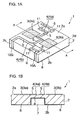
- Fig. 1A schematically shows an antenna with an integral RF circuit, which characterizes a radio apparatus according to a first preferred embodiment
- Fig. 1B shows a schematic sectional view taken along line A-A in Fig. 1A.
- the radio apparatus except for the antenna with the integral RF circuit, which will be described below, may use any construction, and description of the construction of the radio apparatus, except for the antenna with the integral RF circuit, will be omitted herein.
- An antenna 1 with an integral RF circuit includes a dielectric base 2.
- a top surface 2a of the dielectric base 2 preferably is a substantially flat surface without concavities and convexities.
- a plurality of radiation electrodes 3 (3a and 3b) is arranged to be spaced from each other.
- the radiation electrodes 3a and 3b preferably have different resonant frequencies from each other. For example, the radiation electrode 3a on one side is dedicated for reception and the radiation electrode 3b on the other side is dedicated for transmission.
- an integral RF circuit 4 (4a) associated with the radiation electrode 3a and an integral RF circuit 4 (4b) associated with the radiation electrode 3b are disposed on the top surface 2a of the dielectric base 2.
- the RF circuits 4a and 4b include matching circuits constituted of circuit patterns 5, and also include circuit components (e.g., switching elements such as FETs) 6.
- the circuit pattern 5 of each of the RF circuits 4a and 4b is arranged so as to be disposed partially in a gap between the radiation electrodes 3a and 3b, the circuit pattern 5 of the RF circuit 4a being connected to the radiation electrode 3a and the circuit pattern 5 of the RF circuit 4b being connected to the radiation electrode 3b each via a capacitor.
- wiring patterns 10A and 10B for connecting the RF circuit 4b to external circuits are provided on a side surface 2c of the dielectric base 2.
- a wiring pattern (not shown) for connecting the RF circuit 4a to an external circuit is provided on a side surface 2c of the dielectric base 2.
- a concavity 7 is formed in a region corresponding to an area where the circuit patterns 5 of the RF circuits 4a and 4b are formed. That is, in the first preferred embodiment, a thin portion and thick portions are formed in the dielectric base 2 due to the concavity 7.
- the circuit patterns 5 are disposed on a top surface of the thin portion of the dielectric base 2, while the radiation electrodes 3a and 3b are respectively disposed on the thick portions of the dielectric base 2.
- a ground electrode 8 is disposed substantially over the entire bottom surface 2b of the dielectric base 2 and inner surface of the concavity 7.
- the portion where the circuit patterns 5 are provided is constructed in the form of a laminate unit including a ground member, a dielectric member, and a conductor pattern, thus defining a microstrip line structure.
- the antenna 1 with an integral RF circuit is preferably constructed as described above.
- the antenna 1 with an integral RF circuit is surface-mounted, for example, on a circuit board of a communication apparatus, with the bottom surface 2b of the dielectric base 2 defining a mounting surface.
- the wiring pattern 10A of the antenna 1 with the integral RF circuit is conductively connected to a transmission circuit disposed on the circuit board, while the wiring pattern 10B is connected to a bias portion of the circuit board.
- the wiring pattern on the side surface 2d of the dielectric base 2 is conductively connected to a reception circuit on the circuit board.
- the radiation electrode 3b When a signal to be transmitted is supplied from the transmission circuit on the circuit board to the radiation electrode 3b via the wiring pattern 10A and via the circuit component 6 and the circuit pattern 5 (matching circuit) of the RF circuit 4b, the radiation electrode 3b resonates, radiating a radio wave.
- the radiation electrode 3a receives a radio wave, a corresponding reception signal is transferred to the reception circuit on the circuit board via the circuit pattern 5 (matching circuit) and the circuit component 6 of the RF circuit 4a and via the wiring pattern on the side surface 2d.
- the circuit components 6 are switching elements such as FETs, and for example, switching of the switching elements is controlled by a control circuit provided on the circuit board of the communication apparatus.
- a control circuit provided on the circuit board of the communication apparatus.
- dielectric base 2 On the dielectric base 2, through holes conductively connecting the switching elements and the control circuit on the circuit board are disposed.
- top electrodes 11 are connected through to the through holes.
- the radiation electrodes 3a and 3b are arranged to be spaced from each other, on the substantially flat top surface 2a of the dielectric base 2, and the RF circuits 4 are arranged so as to be disposed at least partially in the gap between the radiation electrodes 3a and 3b.
- the radiation electrodes 3a and 3b are separated by such a space where the RF circuits 4a and 4b are partially formed, ensuring isolation between the radiation electrodes 3a and 3b.
- the portion of the dielectric base 2 between the radiation electrodes 3a and 3b is made thin due to the concavity 7, so that electromagnetic coupling between the radiation electrodes 3a and 3b is minimized. This also significantly contributes to ensure isolation between the radiation electrodes 3a and 3b.
- the RF circuits 4 as well as the radiation electrodes 3a and 3b are able to disposed on the dielectric base 2 while preventing any increase in the size of the dielectric base 2. Because an increase in the size of the dielectric base 2 is prevented as described above, an increase in cost is also prevented.
- the RF circuits 4 are disposed on the dielectric base 2 of the antenna 1, the RF circuits 4 need not be disposed on the circuit board of the communication apparatus, thereby allowing the circuit board to be made smaller and thus, reducing the size of the communication apparatus.
- the concavity 7 is formed in the bottom surface of the dielectric base 2, when the antenna 1 with an integral RF circuit, according to the first preferred embodiment, is mounted on the circuit board, a space surrounded by the concavity 7 of the dielectric base 2 and by the circuit board is provided.
- circuit patterns and circuit components may be mounted to define circuits (e.g., baseband circuits conductively connected to the RF circuits 4) on a portion of the circuit board surrounded by the concavity 7, thereby highly efficiently utilizing the space defined by the concavity 7.
- the circuits as well as the antenna 1 are capable of being disposed in an area where the antenna 1 is mounted, allowing the circuit board to be much smaller.
- This unique construction further facilitates reduction in the size of the communication apparatus.
- the radiation electrodes 3 and the RF circuits 4 connected to the radiation electrodes 3 are preferably disposed on the same surface of the dielectric base 2.
- the radiation electrodes 3 and the RF circuits 4 are in proximity to each other, thereby reducing conduction loss.
- the portions of the dielectric base 2 where the radiation electrodes 3 are disposed are made thick, so that the radiation electrodes 3 resonate favorably to transmit or receive radio waves with excellent sensitivity. Furthermore, the portion of the dielectric base 2 where the circuit patterns 5 of the RF circuits 4 are disposed is made thin, so that resonance of the circuit patterns 5 is prevented and minimized due to the associated portion of the dielectric base 2 being thin. Accordingly, radiation loss attributed to radiation of radio waves from the circuit patterns 5 is reduced.
- a communication apparatus is characterized in that an antenna module to be described below is provided, and the communication apparatus, except for the antenna module, may use any construction, and thus description of the construction of the communication apparatus, except for the antenna module, will be omitted herein.
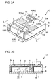
- Fig. 2A is a schematic perspective view showing an example of antenna module characterizing the second preferred embodiment
- Fig. 2B is a schematic sectional view taken along B-B in Fig. 2A.
- the antenna 1 with an integral RF circuit according to the first preferred embodiment, is joined with a substrate 16, with the bottom surface of the dielectric base 2 functioning as a connecting surface. Since the construction of the antenna 1 with an integral RF circuit has been described in relation to the first preferred embodiment, repeated description of common elements will be omitted in the description of the second preferred embodiment.
- the concavity 7 On the bottom surface of the antenna 1 with an integral RF circuit, the concavity 7 is formed. Furthermore, on the substrate 16, circuit patterns (not shown) and circuit components 17 are provided to define circuits 18 in an area surrounded by the concavity 7. The circuits 18 are conductively connected to the RF circuits 4 of the antenna 1 with the integral RF circuit, via the wiring patterns 10A and 10B, etc., which constitute a connecting member.
- Circuits relating to transmission or reception of radio waves include, for example, a signal processing circuit such as a baseband circuit, and a frequency conversion circuit, which is provided as required.
- circuits selected as appropriate from those circuits are disposed on the substrate 16 to define the circuits 18.
- the concavity 7 is provided on the bottom surface of the dielectric base 2 of the antenna 1 with the integral RF circuit, so that a space is formed in the bottom surface of the dielectric base 2.
- the antenna module 15 is constructed efficiently using the space. That is, the substrate 16 is joined with the bottom surface of the antenna 1 with an integral RF circuit, and the circuits 18 are disposed on the substrate 16, in the area surrounded by the concavity 7 on the bottom surface of the antenna 1 with the integral RF circuit. Accordingly, a compact antenna module having a very simple structure is provided.
- circuits such as a frequency conversion circuit and a signal processing circuit are disposed in an area where the antenna 1 with the integral RF circuit is mounted on the circuit board of the communication apparatus, an area for defining the circuits need not be provided separately from the antenna mounting area, allowing the circuit board of the communication apparatus to be made much smaller, thus facilitating reduction in the size of the communication apparatus.
- the ground electrode 8 is disposed substantially over the entire inner surface of the concavity 7 of the dielectric base 2, so that the circuits 18 included in the antenna 1 are covered by the ground electrode 8.
- the circuits 18 included in the antenna 1 are shielded by the ground electrode 8. That is, the ground electrode 8 constitutes a shielding device for the circuits 18. Accordingly, the circuits 18 included in the antenna 1 are not susceptible to negative effects of external electromagnetic waves, and thus operation of the circuits 18 is stabilized.
- the present invention is not limited to preferred embodiments described above, and may be implemented in various forms.
- the RF circuits 4 disposed on the dielectric base 2 are not limited to specific circuit configurations, and may be implemented in any appropriate circuit configurations.
- the circuit patterns 5 of the RF circuits 4 are not limited to the configurations shown in Figs. 1A and 1B and Figs. 2A and 2B.
- the circuit patterns 5 may be conductively connected directly to the radiation electrodes 3.
- the circuit components 6 provided on the dielectric base 2 are switching elements in the preferred embodiments described above, it is to be understood that circuit components other than switching elements may be mounted on the dielectric base 2.
- the shapes of circuit patterns and the types and number of circuit components disposed on the top surface of the dielectric base 2 are determined as appropriate in accordance with the circuit configurations of the RF circuits 4.
- the number of the radiation electrodes 3 provided on the dielectric base 2 is preferably two in the preferred embodiments described above, the number of radiation electrodes 3 may be three or larger, without limitation as long as the number is greater than one.
- the RF circuits 4a and 4b respectively associated one to one with the radiation electrodes 3a and 3b are provided in preferred embodiments described above, for example, in the case of such an arrangement that another radiation electrode for reception is disposed on the dielectric base 2 in addition to the radiation electrode 3a for reception and the radiation electrode 3b for transmission, the radiation electrode for reception being connected to a reception circuit commonly with the radiation electrode 3a, an integral RF circuit common to these radiation electrodes for reception may be provided. As described above, RF circuits need not be provided respectively in one to one association with radiation electrodes.
- the dielectric base 2 is not limited to a specific shape, and may be implemented in any appropriate shape.
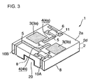
- an opening 20 connected through to the concavity 7 may be provided on a side surface of the dielectric base 2.
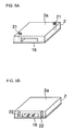
- the dielectric base 2 may be substantially cylindrical, as shown in Fig. 4A.
- Fig. 4B is a diagram showing the substantially cylindrical dielectric base 2 as viewed from the bottom side. As shown in Fig. 4B, no matter what the shape of the dielectric base 2 may be like, the concavity 7 is formed on the bottom surface of the dielectric base 2 so that at least portions of the dielectric base 2 where the radiation electrodes 3 are disposed will be thick.
- the wiring patterns 10 are disposed on a side surface of the dielectric base 2 as a connecting member for connecting the RF circuits 4 disposed on the dielectric base 2 to other circuits in the preferred embodiments described above, for example, through holes may be used as a connecting member.
- metallic pins 21 disposed so as to penetrate through the dielectric base 2 from the top surface 2a to the bottom surface may be provided as the connecting member. In that case, the reliability of connection is improved as compared with a case where wiring patterns are used as the connecting member.
- side-surface electrodes 22 using through holes may be provided as the connecting member.
- a radiation electrode dedicated for reception and a radiation electrode dedicated for transmission are provided on the dielectric base 2 in the preferred embodiments described above, all of a plurality of radiation electrodes disposed on the dielectric base 2 may be dedicated for reception or dedicated for transmission, or used both for transmission and reception. Furthermore, a radiation electrode dedicated for reception, a radiation electrode dedicated for transmission, and a radiation electrode for both transmission and reception may be combined as appropriate.
Landscapes
- Engineering & Computer Science (AREA)
- Computer Networks & Wireless Communication (AREA)
- Waveguide Aerials (AREA)
- Details Of Aerials (AREA)
- Support Of Aerials (AREA)
- Variable-Direction Aerials And Aerial Arrays (AREA)
Abstract

Description
Claims (18)
- An antenna with an integral RF circuit, comprising:a dielectric base 2 having a bottom surface and a top surface that is substantially flat;a plurality of radiation electrodes 3a, 3b for at least one of transmission and reception of a radio wave, disposed on the top surface 2a of the dielectric base 2 and spaced from each other;an RF circuit 4 having a circuit pattern 5 and connected to at least one of the plurality of radiation electrodes 3a, 3b conductively or via a capacitor, the RF circuit 4 being disposed at least partially in a gap between the plurality of radiation electrodes 3a, 3b;a concavity 7 formed in the bottom surface of the dielectric base 2 in a region corresponding to an area where the circuit pattern 5 of the RF circuit 4 is located, the concavity 7 defining a thin portion and a thick portion in the dielectric base 2, the circuit pattern 5 of the RF circuit 4 being disposed on the thin portion of the dielectric base 2 and the plurality of radiation electrodes 3a, 3b being disposed on the thick portion of the dielectric base 2; anda ground electrode 8 disposed on the bottom surface of the dielectric base 2 and on an inner surface of the concavity 7.
- An antenna according to Claim 1, wherein each of the plurality of radiation electrodes 3a, 3b has a different resonant frequency from that of the others of the plurality of radiation electrodes 3a, 3b.
- An antenna according to Claim 1 or 2, wherein the plurality of radiation electrodes 3a, 3b disposed on the top surface 2a of the dielectric base 2 includes at least one radiation electrode dedicated for reception and at least one radiation electrode dedicated for transmission.
- An antenna according to any of Claims 1 to 3, wherein the RF circuit 4 is provided in one-to-one association with each of the plurality of radiation electrodes 3a, 3b.
- An antenna according to any of Claims 1 to 4, further comprising a plurality of the RF circuits 4 disposed partially in the gap between the plurality of radiation electrodes 3a, 3b and a circuit pattern 5 defining a matching circuit 5 disposed between the plurality of RF circuits 4.
- An antenna according to Claim 5, wherein the matching circuit 5 is at least partially located in the gap between the plurality of radiation electrodes 3a, 3b.
- An antenna according to Claim 5, wherein the matching circuit includes switching elements 6.
- An antenna module comprising:a substrate 16;an antenna with an integral RF circuit including:wherein the antenna is joined to the substrate 16 with the bottom surface thereof functioning as a connecting surface;a dielectric base 2 having a bottom surface and a top surface 2a that is substantially flat;a plurality of radiation electrodes 3a, 3b for at least one of transmission and reception of a radio wave, disposed on the top surface 2a of the dielectric base 2 and spaced from each other;an RF circuit 4 having a circuit pattern 5 and connected to at least one of the plurality of radiation electrodes 3a, 3b conductively or via a capacitor, the RF circuit 4 being disposed at least partially in a gap between the plurality of radiation electrodes 3a, 3b;a concavity 7 formed in the bottom surface of the dielectric base 2 in a region corresponding to an area where the circuit pattern 5 of the RF circuit 4 is located, the concavity 7 defining a thin portion and a thick portion in the dielectric base 2, the circuit pattern 5 of the RF circuit 4 being disposed on the thin portion of the dielectric base 2 and the plurality of radiation electrodes 3a, 3b being disposed on the thick portion of the dielectric base 2; anda ground electrode 8 disposed on the bottom surface of the dielectric base 2 and on an inner surface of the concavity 7;a circuit 18 conductively connected to the RF circuit 4 of the antenna and disposed in an area on the substrate 16 surrounded by the concavity 7 on the bottom surface of the antenna; anda connecting member 10a, 10b; 22, 21 for conductively connecting the circuit 18 and the RF circuit 4.
- An antenna module according to Claim 8, wherein the connecting member 22, 21 includes a through hole 22 disposed in the dielectric base 2 of the antenna.
- An antenna module according to Claim 8 or 9, wherein the connecting member includes a wiring pattern 10a, 10b disposed on a side surface of the dielectric base 2 of the antenna.
- An antenna module according to any of Claims 8 to 10, wherein the connecting member 22, 21 includes a metallic pin 21 disposed so as to penetrate through the dielectric base 2 of the antenna from the top surface 2a to the bottom surface.
- An antenna module according to any of Claims 8 to 10, wherein each of the plurality of radiation electrodes 3a, 3b has a different resonant frequency from that of the others of the plurality of radiation electrodes 3a, 3b.
- An antenna module according to any of Claims 8 to 11, wherein the plurality of radiation electrodes 3a, 3b disposed on the top surface 2a of the dielectric base 2 includes at least one radiation electrode 3a, 3b dedicated for reception and at least one radiation electrode dedicated for transmission.
- An antenna module according to any of Claims 8 to 13, wherein the RF 4 circuit is provided in one-to-one association with each of the plurality of radiation electrodes 3a, 3b.
- An antenna module according to any of Claims 8 to 14, further comprising a plurality of the RF circuits 4 disposed partially in the gap between the plurality of radiation electrodes 3a, 3b and a circuit pattern 5 defining a matching circuit disposed between the plurality of RF circuits 4.
- An antenna module according to Claim 15, wherein the matching circuit is at least partially located in the gap between the plurality of radiation electrodes 3a, 3b.
- An antenna module according to Claim 15, wherein the matching circuit includes switching elements.
- A communication apparatus comprising an antenna with an integral RF circuit according to any of Claims 1 to 7.
Applications Claiming Priority (2)
| Application Number | Priority Date | Filing Date | Title |
|---|---|---|---|
| JP2001239303A JP3649168B2 (en) | 2001-08-07 | 2001-08-07 | RF circuit integrated antenna, antenna module using the same, and communication device including the same |
| JP2001239303 | 2001-08-07 |
Publications (3)
| Publication Number | Publication Date |
|---|---|
| EP1289052A2 true EP1289052A2 (en) | 2003-03-05 |
| EP1289052A3 EP1289052A3 (en) | 2004-01-14 |
| EP1289052B1 EP1289052B1 (en) | 2005-03-09 |
Family
ID=19070075
Family Applications (1)
| Application Number | Title | Priority Date | Filing Date |
|---|---|---|---|
| EP02017815A Expired - Lifetime EP1289052B1 (en) | 2001-08-07 | 2002-08-07 | Antenna with an integral RF circuit, antenna module and communication apparatus incorporating the same |
Country Status (4)
| Country | Link |
|---|---|
| US (1) | US6646609B2 (en) |
| EP (1) | EP1289052B1 (en) |
| JP (1) | JP3649168B2 (en) |
| DE (1) | DE60203150T2 (en) |
Cited By (1)
| Publication number | Priority date | Publication date | Assignee | Title |
|---|---|---|---|---|
| WO2005043675A1 (en) | 2003-10-27 | 2005-05-12 | Robert Bosch Gmbh | Antenna assembly, in particular for radar applications in motor vehicles |
Families Citing this family (27)
| Publication number | Priority date | Publication date | Assignee | Title |
|---|---|---|---|---|
| DE10113349A1 (en) * | 2001-03-20 | 2002-09-26 | Philips Corp Intellectual Pty | Antenna with substrate and conducting track has at least one aperture formed by hollow chamber enclosed by substrate or by recess formed in one or more surfaces of substrate |
| EP1563570A1 (en) | 2002-11-07 | 2005-08-17 | Fractus, S.A. | Integrated circuit package including miniature antenna |
| JP2004274418A (en) * | 2003-03-10 | 2004-09-30 | Tdk Corp | Antenna integrated module |
| EP1771919A1 (en) * | 2004-07-23 | 2007-04-11 | Fractus, S.A. | Antenna in package with reduced electromagnetic interaction with on chip elements |
| US7924226B2 (en) * | 2004-09-27 | 2011-04-12 | Fractus, S.A. | Tunable antenna |
| JP4725582B2 (en) * | 2005-10-27 | 2011-07-13 | 株式会社村田製作所 | High frequency module |
| US7683839B2 (en) * | 2006-06-30 | 2010-03-23 | Nokia Corporation | Multiband antenna arrangement |
| CN101227202B (en) * | 2007-01-19 | 2011-07-27 | 鸿富锦精密工业(深圳)有限公司 | electronic device |
| US7760142B2 (en) * | 2007-04-10 | 2010-07-20 | Emag Technologies, Inc. | Vertically integrated transceiver array |
| US8878727B2 (en) * | 2009-02-12 | 2014-11-04 | Origin Gps Ltd. | Antenna-module hybrid circuit |
| JP2012253436A (en) * | 2011-05-31 | 2012-12-20 | Tdk Corp | Triple band antenna device and radio communication apparatus using the same |
| JP6168394B2 (en) * | 2013-05-02 | 2017-07-26 | 三菱マテリアル株式会社 | Antenna device |
| USD757693S1 (en) * | 2013-09-26 | 2016-05-31 | Murata Manufacturing Co., Ltd. | Wireless transmission/reception module |
| USD892774S1 (en) * | 2013-09-26 | 2020-08-11 | Murata Manufacturing Co., Ltd. | Wireless transmission/reception module |
| JP6238239B2 (en) * | 2014-11-27 | 2017-11-29 | アルプス電気株式会社 | Communication module |
| WO2016120254A1 (en) * | 2015-01-27 | 2016-08-04 | At & S Austria Technologie & Systemtechnik Aktiengesellschaft | Component carrier with integrated antenna structure |
| USD768115S1 (en) * | 2015-02-05 | 2016-10-04 | Armen E. Kazanchian | Module |
| US10971806B2 (en) | 2017-08-22 | 2021-04-06 | The Boeing Company | Broadband conformal antenna |
| US11233310B2 (en) * | 2018-01-29 | 2022-01-25 | The Boeing Company | Low-profile conformal antenna |
| JP2019176202A (en) * | 2018-03-26 | 2019-10-10 | 富士通コンポーネント株式会社 | Wireless module |
| KR102767861B1 (en) | 2018-04-03 | 2025-02-18 | 코닝 인코포레이티드 | Electronic package comprising structured glass article and method for manufacturing same |
| US10916853B2 (en) | 2018-08-24 | 2021-02-09 | The Boeing Company | Conformal antenna with enhanced circular polarization |
| US10923831B2 (en) | 2018-08-24 | 2021-02-16 | The Boeing Company | Waveguide-fed planar antenna array with enhanced circular polarization |
| US10938082B2 (en) | 2018-08-24 | 2021-03-02 | The Boeing Company | Aperture-coupled microstrip-to-waveguide transitions |
| WO2021000071A1 (en) * | 2019-06-29 | 2021-01-07 | 瑞声声学科技(深圳)有限公司 | Antenna module and mobile terminal |
| US11276933B2 (en) | 2019-11-06 | 2022-03-15 | The Boeing Company | High-gain antenna with cavity between feed line and ground plane |
| WO2022230427A1 (en) | 2021-04-28 | 2022-11-03 | 株式会社村田製作所 | Antenna device |
Family Cites Families (6)
| Publication number | Priority date | Publication date | Assignee | Title |
|---|---|---|---|---|
| JPH114113A (en) * | 1997-04-18 | 1999-01-06 | Murata Mfg Co Ltd | Surface mount antenna and communication apparatus using the same |
| JPH1168456A (en) * | 1997-08-19 | 1999-03-09 | Murata Mfg Co Ltd | Surface mounting antenna |
| EP1152485B1 (en) * | 1999-02-15 | 2014-06-18 | National Institute of Information and Communications Technology | Radio communication device |
| JP2000278009A (en) * | 1999-03-24 | 2000-10-06 | Nec Corp | Microwave / millimeter wave circuit device |
| TW431033B (en) * | 1999-09-03 | 2001-04-21 | Ind Tech Res Inst | Twin-notch loaded type microstrip antenna |
| DE60033275T2 (en) * | 1999-09-09 | 2007-10-25 | Murata Manufacturing Co., Ltd., Nagaokakyo | SURFACE MOUNTABLE ANTENNA AND COMMUNICATION DEVICE WITH SUCH ANTENNA |
-
2001
- 2001-08-07 JP JP2001239303A patent/JP3649168B2/en not_active Expired - Fee Related
-
2002
- 2002-07-08 US US10/189,424 patent/US6646609B2/en not_active Expired - Fee Related
- 2002-08-07 EP EP02017815A patent/EP1289052B1/en not_active Expired - Lifetime
- 2002-08-07 DE DE60203150T patent/DE60203150T2/en not_active Expired - Lifetime
Cited By (2)
| Publication number | Priority date | Publication date | Assignee | Title |
|---|---|---|---|---|
| WO2005043675A1 (en) | 2003-10-27 | 2005-05-12 | Robert Bosch Gmbh | Antenna assembly, in particular for radar applications in motor vehicles |
| US7696938B2 (en) | 2003-10-27 | 2010-04-13 | Robert Bosch Gmbh | Antenna system, particularly for radar applications in motor vehicles |
Also Published As
| Publication number | Publication date |
|---|---|
| JP3649168B2 (en) | 2005-05-18 |
| US6646609B2 (en) | 2003-11-11 |
| EP1289052A3 (en) | 2004-01-14 |
| DE60203150T2 (en) | 2006-05-11 |
| US20030030587A1 (en) | 2003-02-13 |
| JP2003051711A (en) | 2003-02-21 |
| EP1289052B1 (en) | 2005-03-09 |
| DE60203150D1 (en) | 2005-04-14 |
Similar Documents
| Publication | Publication Date | Title |
|---|---|---|
| EP1289052B1 (en) | Antenna with an integral RF circuit, antenna module and communication apparatus incorporating the same | |
| JP3639767B2 (en) | Surface mount antenna and communication device using the same | |
| US6876328B2 (en) | Multiple-resonant antenna, antenna module, and radio device using the multiple-resonant antenna | |
| EP1368858B1 (en) | Module and electronic device | |
| FI114259B (en) | Structure of a radio frequency front end | |
| US6046703A (en) | Compact wireless transceiver board with directional printed circuit antenna | |
| US7057558B2 (en) | Antenna device | |
| EP1307942B1 (en) | Antenna device | |
| US6195049B1 (en) | Micro-strip patch antenna for transceiver | |
| CN111279548B (en) | Communication device | |
| JP2004201278A (en) | Pattern antenna | |
| JP2002076735A (en) | Pattern antenna and wireless communication device having the same | |
| JP2004096206A (en) | Waveguide / planar line converter, and high frequency circuit apparatus | |
| JP2008177888A (en) | Multi-frequency antenna | |
| US5969680A (en) | Antenna device having a radiating portion provided between a wiring substrate and a case | |
| US6697023B1 (en) | Built-in multi-band mobile phone antenna with meandering conductive portions | |
| US20240145893A1 (en) | Radio frequency filters covered by printed circuit boards | |
| US20080272964A1 (en) | Antenna Radiator Assembly and Radio Communications Assembly | |
| US11888227B2 (en) | Communication device | |
| JP2001094336A (en) | Patch antenna incorporating filter | |
| JPH07249927A (en) | Surface mounted antenna | |
| JP2004221714A (en) | Dielectric waveguide antenna | |
| CN210379412U (en) | Antenna, antenna assembly and electronic equipment | |
| TWI920589B (en) | Antenna device | |
| JP2003309423A (en) | Antenna integrated high frequency circuit module |
Legal Events
| Date | Code | Title | Description |
|---|---|---|---|
| PUAI | Public reference made under article 153(3) epc to a published international application that has entered the european phase |
Free format text: ORIGINAL CODE: 0009012 |
|
| 17P | Request for examination filed |
Effective date: 20020807 |
|
| AK | Designated contracting states |
Kind code of ref document: A2 Designated state(s): AT BE BG CH CY CZ DE DK EE ES FI FR GB GR IE IT LI LU MC NL PT SE SK TR |
|
| AX | Request for extension of the european patent |
Extension state: AL LT LV MK RO SI |
|
| PUAL | Search report despatched |
Free format text: ORIGINAL CODE: 0009013 |
|
| AK | Designated contracting states |
Kind code of ref document: A3 Designated state(s): AT BE BG CH CY CZ DE DK EE ES FI FR GB GR IE IT LI LU MC NL PT SE SK TR |
|
| AX | Request for extension of the european patent |
Extension state: AL LT LV MK RO SI |
|
| GRAP | Despatch of communication of intention to grant a patent |
Free format text: ORIGINAL CODE: EPIDOSNIGR1 |
|
| AKX | Designation fees paid |
Designated state(s): DE ES FR GB IT |
|
| GRAS | Grant fee paid |
Free format text: ORIGINAL CODE: EPIDOSNIGR3 |
|
| GRAA | (expected) grant |
Free format text: ORIGINAL CODE: 0009210 |
|
| AK | Designated contracting states |
Kind code of ref document: B1 Designated state(s): DE ES FR GB IT |
|
| PG25 | Lapsed in a contracting state [announced via postgrant information from national office to epo] |
Ref country code: IT Free format text: LAPSE BECAUSE OF FAILURE TO SUBMIT A TRANSLATION OF THE DESCRIPTION OR TO PAY THE FEE WITHIN THE PRESCRIBED TIME-LIMIT;WARNING: LAPSES OF ITALIAN PATENTS WITH EFFECTIVE DATE BEFORE 2007 MAY HAVE OCCURRED AT ANY TIME BEFORE 2007. THE CORRECT EFFECTIVE DATE MAY BE DIFFERENT FROM THE ONE RECORDED. Effective date: 20050309 |
|
| REG | Reference to a national code |
Ref country code: GB Ref legal event code: FG4D |
|
| REF | Corresponds to: |
Ref document number: 60203150 Country of ref document: DE Date of ref document: 20050414 Kind code of ref document: P |
|
| PG25 | Lapsed in a contracting state [announced via postgrant information from national office to epo] |
Ref country code: ES Free format text: LAPSE BECAUSE OF FAILURE TO SUBMIT A TRANSLATION OF THE DESCRIPTION OR TO PAY THE FEE WITHIN THE PRESCRIBED TIME-LIMIT Effective date: 20050620 |
|
| PLBE | No opposition filed within time limit |
Free format text: ORIGINAL CODE: 0009261 |
|
| STAA | Information on the status of an ep patent application or granted ep patent |
Free format text: STATUS: NO OPPOSITION FILED WITHIN TIME LIMIT |
|
| 26N | No opposition filed |
Effective date: 20051212 |
|
| ET | Fr: translation filed | ||
| PGFP | Annual fee paid to national office [announced via postgrant information from national office to epo] |
Ref country code: DE Payment date: 20100812 Year of fee payment: 9 Ref country code: FR Payment date: 20100824 Year of fee payment: 9 |
|
| PGFP | Annual fee paid to national office [announced via postgrant information from national office to epo] |
Ref country code: GB Payment date: 20100811 Year of fee payment: 9 |
|
| GBPC | Gb: european patent ceased through non-payment of renewal fee |
Effective date: 20110807 |
|
| REG | Reference to a national code |
Ref country code: FR Ref legal event code: ST Effective date: 20120430 |
|
| REG | Reference to a national code |
Ref country code: DE Ref legal event code: R119 Ref document number: 60203150 Country of ref document: DE Effective date: 20120301 |
|
| PG25 | Lapsed in a contracting state [announced via postgrant information from national office to epo] |
Ref country code: GB Free format text: LAPSE BECAUSE OF NON-PAYMENT OF DUE FEES Effective date: 20110807 Ref country code: FR Free format text: LAPSE BECAUSE OF NON-PAYMENT OF DUE FEES Effective date: 20110831 |
|
| PG25 | Lapsed in a contracting state [announced via postgrant information from national office to epo] |
Ref country code: DE Free format text: LAPSE BECAUSE OF NON-PAYMENT OF DUE FEES Effective date: 20120301 |