EP1289047A1 - Circulators with a common matching structure - Google Patents
Circulators with a common matching structure Download PDFInfo
- Publication number
- EP1289047A1 EP1289047A1 EP02255390A EP02255390A EP1289047A1 EP 1289047 A1 EP1289047 A1 EP 1289047A1 EP 02255390 A EP02255390 A EP 02255390A EP 02255390 A EP02255390 A EP 02255390A EP 1289047 A1 EP1289047 A1 EP 1289047A1
- Authority
- EP
- European Patent Office
- Prior art keywords
- circulator
- ferrite
- permanent magnet
- junctions
- component
- Prior art date
- Legal status (The legal status is an assumption and is not a legal conclusion. Google has not performed a legal analysis and makes no representation as to the accuracy of the status listed.)
- Ceased
Links
- 229910000859 α-Fe Inorganic materials 0.000 claims abstract description 75
- 230000005540 biological transmission Effects 0.000 claims abstract description 52
- 239000004020 conductor Substances 0.000 claims abstract description 44
- 239000002184 metal Substances 0.000 claims abstract description 18
- 229910052751 metal Inorganic materials 0.000 claims abstract description 18
- 230000005291 magnetic effect Effects 0.000 claims description 23
- 238000000034 method Methods 0.000 claims description 4
- 238000004519 manufacturing process Methods 0.000 claims 1
- 230000009977 dual effect Effects 0.000 abstract description 52
- 238000002955 isolation Methods 0.000 description 12
- 238000013459 approach Methods 0.000 description 6
- 239000000463 material Substances 0.000 description 5
- 230000007704 transition Effects 0.000 description 5
- 238000013461 design Methods 0.000 description 4
- 230000035945 sensitivity Effects 0.000 description 4
- XEEYBQQBJWHFJM-UHFFFAOYSA-N Iron Chemical compound [Fe] XEEYBQQBJWHFJM-UHFFFAOYSA-N 0.000 description 2
- 230000004907 flux Effects 0.000 description 2
- 238000003780 insertion Methods 0.000 description 2
- 230000037431 insertion Effects 0.000 description 2
- RYGMFSIKBFXOCR-UHFFFAOYSA-N Copper Chemical compound [Cu] RYGMFSIKBFXOCR-UHFFFAOYSA-N 0.000 description 1
- 229910000831 Steel Inorganic materials 0.000 description 1
- 239000000919 ceramic Substances 0.000 description 1
- 229910052802 copper Inorganic materials 0.000 description 1
- 239000010949 copper Substances 0.000 description 1
- 238000005530 etching Methods 0.000 description 1
- 239000003302 ferromagnetic material Substances 0.000 description 1
- 239000011888 foil Substances 0.000 description 1
- 230000001939 inductive effect Effects 0.000 description 1
- 229910052742 iron Inorganic materials 0.000 description 1
- 239000000696 magnetic material Substances 0.000 description 1
- 238000012986 modification Methods 0.000 description 1
- 230000004048 modification Effects 0.000 description 1
- AJCDFVKYMIUXCR-UHFFFAOYSA-N oxobarium;oxo(oxoferriooxy)iron Chemical compound [Ba]=O.O=[Fe]O[Fe]=O.O=[Fe]O[Fe]=O.O=[Fe]O[Fe]=O.O=[Fe]O[Fe]=O.O=[Fe]O[Fe]=O.O=[Fe]O[Fe]=O AJCDFVKYMIUXCR-UHFFFAOYSA-N 0.000 description 1
- 238000000206 photolithography Methods 0.000 description 1
- 230000008569 process Effects 0.000 description 1
- 239000010959 steel Substances 0.000 description 1
Images




Classifications
-
- H—ELECTRICITY
- H01—ELECTRIC ELEMENTS
- H01P—WAVEGUIDES; RESONATORS, LINES, OR OTHER DEVICES OF THE WAVEGUIDE TYPE
- H01P1/00—Auxiliary devices
- H01P1/32—Non-reciprocal transmission devices
- H01P1/38—Circulators
- H01P1/383—Junction circulators, e.g. Y-circulators
- H01P1/387—Strip line circulators
Definitions
- the present invention relates generally to radio frequency and microwave circulators, and more specifically to a junction-type stripline circulator providing enhanced performance in a more compact device configuration.
- Radio Frequency (RF) and microwave circulators are known that employ a DC-biasing magnetic field generated in ferrite material enveloping a conductor to provide at least one non-reciprocal transmission path between signal ports on a network.
- a conventional junction-type stripline circulator comprises at least one junction configured as an interface between the signal ports.
- Each junction of the junction-type stripline circulator typically includes two (2) permanent magnets, two (2) ground plane portions disposed between the magnets, two (2) ferrite disks disposed between the ground plane portions, a dielectric constant medium disposed between the ferrite disks, and a conductor sandwiched between the ferrite disks and patterned to correspond to the transmission paths between the signal ports.
- the permanent magnets are configured to generate a DC-biasing magnetic field in the ferrite disks, thereby providing the desired non-reciprocal operation of the transmission paths between the signal ports on the network.
- junction-type stripline circulator particularly multi-junction stripline circulators comprising a plurality of junctions connected in cascade
- the successive junctions of the multi-junction stripline circulator are typically interconnected by respective microstrip transmission lines.
- an impedance matching structure is typically required at each junction-to-transmission line transition of the circulator.
- a multi-junction stripline circulator comprising two (2) junctions may include a single transmission line interconnecting the junctions and two (2) impedance matching structures at respective ends of the transmission line.
- VSWR Voltage Standing Wave Ratio
- such a junction-type stripline circulator configuration comprising a transmission line between successive junctions of the circulator and multiple impedance matching structures at the junction-to-transmission line transitions can significantly increase the size of the overall device.
- junction-type stripline circulator that can be used in RF and microwave applications.
- Such a junction-type stripline circulator would be configured to provide enhanced performance in a smaller device configuration.
- a junction-type stripline circulator in which performance is enhanced while the size of the overall device is reduced. Benefits of the presently disclosed invention are achieved by configuring the junction-type stripline circulator to include a single permanent magnet and a dual ferrite component that are employed by successive junctions of the circulator, and a single impedance matching structure coupled between the successive junctions of the circulator.
- the junction-type stripline circulator comprises a compact dual element cascade circulator including a plurality of junctions connected in cascade to provide a plurality of non-reciprocal transmission paths between signal ports on a network.
- the plurality of junctions comprises a single oblong permanent magnet, an oblong ground plane disposed near the permanent magnet, a dual ferrite component including two (2) oblong ferrite elements disposed near the ground plane, and a conductor sandwiched between the ferrite elements.
- a dielectric constant medium is disposed between the two (2) ferrite elements.
- the conductor is patterned to correspond to the configuration of the transmission paths between the signal ports.
- the conductor includes a plurality of conductor portions, and each junction of the dual element cascade circulator comprises a respective one of the conductor portions. Further, sections of the conductor between successive conductor portions are used to form single impedance matching structures for respective junction-to-junction transitions.
- each impedance matching structure comprises a lumped reactance.
- the dual element cascade circulator further includes a metal housing having an open top into which the plurality of junctions is disposed, and a metal cover configured to enclose the top of the housing to secure the junctions inside.
- the metal housing has a plurality of slots through which respective contact terminals of the conductor protrude to make contact with the signal ports on the network.
- the plurality of junctions further comprises two (2) oblong pole pieces associated with the permanent magnet, and a cover return component.
- a first pole piece is disposed between the magnet and the ground plane, and a second pole piece is disposed between the base of the housing and the dual ferrite component.
- the cover return component is disposed between the cover and the permanent magnet.
- the combination of the ground plane, the dual ferrite component, and the conductor forms a Radio Frequency (RF) or microwave circuit configured to provide desired non-reciprocal transmission paths between the network signal ports.
- RF Radio Frequency
- the combination of the pole pieces, the permanent magnet, the metal housing, the cover return component, and the metal cover forms a magnetic circuit configured to generate a DC-biasing magnetic field in the dual ferrite component, thereby achieving the desired non-reciprocal operation of the transmission paths.
- the two (2) pole pieces are configured to enhance the homogeneity of the magnetic field in the dual ferrite component
- the cover return component is configured to provide an easy return path for the magnetic flux associated with the DC-biasing magnetic field from the ferrite elements to the permanent magnet
- each impedance matching structure is configured to avoid the reflection of energy between successive junctions of the circulator.
- the circulator By configuring the compact dual element cascade circulator to include the single permanent magnet and the dual ferrite component that can be employed by successive junctions of the circulator, and the single impedance matching structure coupled between the respective successive junctions, the circulator achieves numerous benefits. For example, the performance of the dual element cascade circulator is enhanced. Particularly, by providing the single impedance matching structure between successive junctions, phase uniformity is improved, and both Voltage Standing Wave Ratio (VSWR) amplitude sensitivity and overall insertion loss are reduced.
- VSWR Voltage Standing Wave Ratio
- a junction-type stripline circulator that provides enhanced performance in a more compact design configuration.
- a single permanent magnet and a dual ferrite component are employed by successive junctions of the circulator, and a single impedance matching structure is coupled between the respective successive junctions, thereby reducing the sensitivity of the phase and Voltage Standing Wave Ratio (VSWR) amplitude between the junctions while reducing the size of the overall device.
- VSWR Voltage Standing Wave Ratio
- Fig. 1 depicts a plan view of an illustrative embodiment of a compact dual element cascade circulator 100 configured to provide a plurality of non-reciprocal transmission paths between signal ports on a network (not shown), in accordance with the present invention.
- the dual element cascade circulator 100 includes an oblong permanent magnet 106, a dual ferrite component 108, a center conductor 110 sandwiched between two (2) oblong ferrite elements of the ferrite component 108, and an oblong cover return component 104.
- the permanent magnet 106, the ferrite component 108, the center conductor 110, and the cover return component 104 are disposed in a metal housing 102 having an open top and a plurality of slots 112a-112d through which respective contact terminals 114a-114d of the center conductor 110 protrude to make contact with, e.g. , four (4) signal ports (not shown) on the network.
- the center conductor 110 may be formed from a thin sheet of foil or copper, or any other suitable electrically conductive material. Further, the center conductor 110 may be patterned to correspond to the transmission paths between the signal ports by way of etching, stamping, photolithography, or any other suitable process.
- the dual element cascade circulator 100 comprises two (2) junctions connected in cascade and configured as an interface between four (4) signal ports. Specifically, a first junction includes a center conductor portion 110a, and a second junction connected in cascade to the first junction at a common conductor section 111 includes a center conductor portion 110b.
- the permanent magnet 106, the ferrite elements of the ferrite component 108, and the cover return component 104 are configured to be shared by both the first and second junctions of the circulator 100. It is understood that the dual element cascade circulator 100 may be configured to accommodate one or more junctions to provide transmission paths between a desired number of network signal ports.
- Fig. 2 depicts an exploded view of the dual element cascade circulator 100 (see also Fig. 1).
- the dual element cascade circulator 100 includes the permanent magnet 106, the ferrite component 108 comprising the ferrite elements 108a and 108b, the center conductor 110, the cover return component 104, and the metal housing 102.
- the permanent magnet 106 operates in conjunction with pole pieces 116a and 116b, which are configured to enhance the homogeneity of a DC-biasing magnetic field generated in the ferrite component 108 by the magnet 106.
- the permanent magnet 106 is disposed between the cover return component 104 and the pole piece 116a, and the pole piece 116b is disposed between the ferrite element 108b and the base of the housing 102.
- the DC-biasing magnetic field may alternatively be generated by a pair of permanent magnets or by an electromagnet.
- the combination of the ferrite elements 108a and 108b, a dielectric constant medium (e.g., air) disposed between the ferrite elements 108a and 108b, the center conductor 110 sandwiched between the ferrite elements 108a and 108b, and a ground plane 114 disposed between the pole piece 116a and the ferrite element 108a forms a Radio Frequency (RF) or microwave circuit, which is configured to provide desired non-reciprocal transmission paths between the four (4) network signal ports when a suitable DC-biasing magnetic field is generated in the ferrite component 108.
- RF Radio Frequency
- the RF or microwave circuit may be configured to transmit power in forward directions along respective transmission paths extending from the contact terminal 114a to the contact terminal 114d, from the contact terminal 114a to the contact terminal 114b, and from the contact terminal 114c to the contact terminal 114b, while preventing the transmission of power in corresponding reverse directions (i.e., the contact terminal 114d is isolated from the contact terminal 114a, the contact terminal 114b is isolated from the contact terminal 114a, and the contact terminal 114b is isolated from the contact terminal 114c). It is understood that the RF or microwave circuit may be configured to transmit power in forward directions and prevent such transmission in corresponding reverse directions along alternative non-reciprocal transmission paths between the network signal ports.
- the combination of the pole pieces 116a and 116b, the permanent magnet 106, the metal housing 102, the cover return component 104, and a metal cover 118 forms a magnetic circuit, which is configured to generate the suitable DC-biasing magnetic field in the ferrite component 108 between the pole pieces 116a and 116b.
- the cover return component 104 is configured to provide an easy return path for the magnetic flux associated with the DC-biasing magnetic field from the ferrite elements 108a and 108b back to the permanent magnet 106.
- the metal housing 102 and the metal cover 118 may be made of iron, steel, or any other suitable ferromagnetic material capable of completing the magnetic circuit between the pole pieces 116a and 116b.
- the dual element cascade circulator 100 comprises the first junction including the center conductor portion 110a and the second junction including the center conductor portion 110b, in which the common conductor section 111 interconnects the center conductor portions 110a and 110b.
- the common conductor section 111 in combination with the ferrite elements 108a and 108b, the dielectric constant medium between the ferrite elements 108a and 108b, and the ground plane 114 of the RF or microwave circuit, is configured to provide a single impedance matching structure for the junction-to-junction transition.
- the single impedance matching structure comprises a lumped reactance.
- the lumped reactance may be suitably configured to obtain any capacitive or inductive reactance needed to avoid the reflection of energy between the successive junctions.
- the lumped reactance is configured to provide an impedance of about 50 ⁇ at the junction-to-junction transition.
- the single impedance matching structure may alternatively comprise a lumped capacitance.
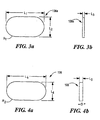
- Fig. 3a depicts a plan view of the ferrite element 108a included in the dual element cascade circulator 100 (see Figs. 1 and 2).
- the ferrite element 108b (see Figs. 1 and 2) has a configuration similar to that of the ferrite element 108a.
- the material used to make the ferrite elements 108a and 108b may be TTVG-1200 or any other suitable material.
- the dimension L 1 is about 35.6 mm (1.400 inches)
- the dimension L 2 is about 17.5 mm (0.690 inches)
- the radius R 1 is about 8.8 mm (0.345 inches).
- the surface finish dimensions/unevenness of the ferrite component 108 are preferably less than about 0.508 ⁇ m (20 ⁇ inches).
- Fig. 3b depicts a side view of the ferrite element 108a shown in Fig. 3a.
- the dimension L 3 is about 1.0 mm (0.040 inches).
- Fig. 4a depicts a plan view of the permanent magnet 106 included in the dual element cascade circulator 100 (see Fig. 1).
- the material used to make the permanent magnet 106 may comprise anisotropic ceramic (barium ferrite) or SSR-360H according to the Magnetic Materials Producers Associates (MMPA) standard specifications, or any other suitable material.
- the dimension L 6 is about 36.7 mm (1.446 inches)
- the dimension L 4 is about 18.7 mm (0.735 inches)
- the radius R 2 is about 9.3 mm (0.367 inches).
- Fig. 4b depicts a side view of the permanent magnet 106.
- the dimension L 5 is about 3.8 mm (0.150 inches).
- the indication "- 0 -" shown in Fig. 4b designates the magnetic orientation of the permanent magnet 106.
- Figs. 5a-5b depict plots representing power transmission versus frequency at the contact terminals 114a and 114b of the dual element cascade circulator 100 (see Fig. 1).
- the RF or microwave circuit of the circulator 100 is configured to transmit power in a forward direction from the contact terminal 114a to the contact terminal 114b, and to provide isolation in a corresponding reverse direction from the contact terminal 114b to the contact terminal 114a. Accordingly, the plot of Fig.
- FIG. 5a shows maximum power transmission at the contact terminal 114b at about the center frequency of an exemplary operating frequency range of 740 MHz to 1100 MHz. Further, the plot of Fig. 5b shows minimum power transmission in a corresponding reverse direction (i.e ., maximum isolation) at the contact terminal 114a at about the center frequency of the exemplary operating frequency range.
- Figs. 5c-5d depict Smith chart plots representing impedance versus frequency, as viewed from the contact terminals 114a and 114b, respectively. As shown in Figs. 5c-5d, the respective impedance values approach 50 ⁇ near the center frequency of the above-defined exemplary operating frequency range.
- Figs. 6a-6b depict plots representing power transmission versus frequency at the contact terminals 114a and 114d of the dual element cascade circulator 100 (see Fig. 1).
- the RF or microwave circuit of the circulator 100 is configured to provide isolation from the contact terminal 114a to the contact terminal 114d, and to provide maximum power from the contact terminal 114d to the contact terminal 114a.
- the plot of Fig. 6a shows maximum power transmission at the contact terminal 114a at about the center frequency of the above-defined exemplary operating frequency range
- the plot of Fig. 6b shows minimum power transmission (i.e., maximum isolation) at the contact terminal 114d at about the center frequency of the exemplary operating frequency range.
- Figs. 6c-6d depict Smith chart plots representing impedance versus frequency, as viewed from the contact terminals 114a and 114d, respectively. As shown in Figs. 6c-6d, the respective impedance values approach 50 ⁇ near the center frequency of the above-defined exemplary operating frequency range.
- Figs. 7a-7b depict plots representing power transmission versus frequency at the contact terminals 114c and 114b of the dual element cascade circulator 100 (see Fig. 1).
- the RF or microwave circuit of the circulator 100 is configured to transmit power in a direction from the contact terminal 114b to the contact terminal 114c, and to provide isolation in a corresponding reverse direction from the contact terminal 114c to the contact terminal 114b.
- the plot of Fig. 7a shows maximum power transmission at the contact terminal 114c at about the center frequency of the above-defined exemplary operating frequency range
- the plot of Fig. 7b shows minimum power transmission (i.e., maximum isolation) at the contact terminal 114b at about the center frequency of the exemplary operating frequency range.
- Figs. 7c-7d depict Smith chart plots representing impedance versus frequency, as viewed from the contact terminals 114c and 114b, respectively. As shown in Figs. 7c-7d, the respective impedance values approach 50 ⁇ near the center frequency of the above-defined exemplary operating frequency range.
- Fig. 8 depicts a plan view of an alternative embodiment of a compact dual element cascade circulator 100a configured to provide a plurality of non-reciprocal transmission paths between signal ports on a network (not shown), in accordance with the present invention.
- the dual element cascade circulator 100a is like the dual element cascade circulator 100 with the exception that the common conductor section 111 (see Fig. 1) of the circulator 100 is replaced by an alternative common conductor section 111a (see Fig. 8).
- Figs. 9a-9b depict plots representing power transmission versus frequency at the contact terminals 114a and 114b of the dual element cascade circulator 100a (see Fig. 8).
- the RF or microwave circuit of the circulator 100a is configured to transmit power in a forward direction from the contact terminal 114a to the contact terminal 114b, and to provide isolation in a corresponding reverse direction from the contact terminal 114b to the contact terminal 114a.
- the plot of Fig. 9a shows maximum power transmission at the contact terminal 114b at about the center frequency of the exemplary operating frequency range of 740 MHz to 1100 MHz.
- the plot of Fig. 9b shows minimum power transmission (i.e. , maximum isolation) at the contact terminal 114a at about the center frequency of the exemplary operating frequency range.
- Figs. 9c-9d depict Smith chart plots representing impedance versus frequency, as viewed from the contact terminals 114a and 114b, respectively. As shown in Figs. 9c-9d, the respective impedance values approach 50 ⁇ near the center frequency of the above-defined exemplary operating frequency range.
- Figs. 10a-10b depict plots representing power transmission versus frequency at the contact terminals 114a and 114d of the dual element cascade circulator 100a (see Fig. 8).
- the RF or microwave circuit of the circulator 100a is configured to transmit power in a direction from the contact terminal 114d to the contact terminal 114a, and to provide isolation in a corresponding reverse direction from the contact terminal 114a to the contact terminal 114d.
- the plot of Fig. 10a shows maximum power transmission at the contact terminal 114a at about the center frequency of the above-defined exemplary operating frequency range
- the plot of Fig. 10b shows minimum power transmission (i.e ., maximum isolation) at the contact terminal 114d at about the center frequency of the exemplary operating frequency range.
- Figs. 10c-10d depict Smith chart plots representing impedance versus frequency, as viewed from the contact terminals 114a and 114d, respectively. As shown in Figs. 10c-10d, the respective impedance values approach 50 ⁇ near the center frequency of the above-defined exemplary operating frequency range.
- Figs. 11a-11b depict plots representing power transmission versus frequency at the contact terminals 114b and 114c of the dual element cascade circulator 100a (see Fig. 8).
- the RF or microwave circuit of the circulator 100a is configured to transmit power in a direction from the contact terminal 114b to the contact terminal 114c, and to provide isolation in a corresponding reverse direction from the contact terminal 114c to the contact terminal 114b.
- the plot of Fig. 11a shows maximum power transmission at the contact terminal 114c at about the center frequency of the above-defined exemplary operating frequency range
- the plot of Fig. 11b shows minimum power transmission (i.e ., maximum isolation) at the contact terminal 114b at about the center frequency of the exemplary operating frequency range.
- Figs. 11c-11d depict Smith chart plots representing impedance versus frequency, as viewed from the contact terminals 114c and 114b, respectively. As shown in Figs. 11c-11d, the respective impedance values approach 50 ⁇ near the center frequency of the above-defined exemplary operating frequency range.
- the compact dual element cascade circulator 100 (see Figs. 1 and 2) to include the single permanent magnet and the dual ferrite component that can be shared by successive junctions of the circulator 100, and the single impedance matching structure coupled between the respective successive junctions, the performance of the circulator 100 is enhanced. Specifically, phase uniformity is improved, and both the VSWR amplitude sensitivity and overall insertion loss are reduced. Further, the size of the overall device comprising the dual element cascade circulator 100 is reduced compared to conventional junction-type stripline circulator configurations.
Landscapes
- Non-Reversible Transmitting Devices (AREA)
- Transceivers (AREA)
Abstract
Description
- The present invention relates generally to radio frequency and microwave circulators, and more specifically to a junction-type stripline circulator providing enhanced performance in a more compact device configuration.
- Radio Frequency (RF) and microwave circulators are known that employ a DC-biasing magnetic field generated in ferrite material enveloping a conductor to provide at least one non-reciprocal transmission path between signal ports on a network. A conventional junction-type stripline circulator comprises at least one junction configured as an interface between the signal ports. Each junction of the junction-type stripline circulator typically includes two (2) permanent magnets, two (2) ground plane portions disposed between the magnets, two (2) ferrite disks disposed between the ground plane portions, a dielectric constant medium disposed between the ferrite disks, and a conductor sandwiched between the ferrite disks and patterned to correspond to the transmission paths between the signal ports. The permanent magnets are configured to generate a DC-biasing magnetic field in the ferrite disks, thereby providing the desired non-reciprocal operation of the transmission paths between the signal ports on the network.
- One drawback of the conventional junction-type stripline circulator, particularly multi-junction stripline circulators comprising a plurality of junctions connected in cascade, is that it frequently exhibits degraded electrical performance. This is because the successive junctions of the multi-junction stripline circulator are typically interconnected by respective microstrip transmission lines. Further, an impedance matching structure is typically required at each junction-to-transmission line transition of the circulator. For example, a multi-junction stripline circulator comprising two (2) junctions may include a single transmission line interconnecting the junctions and two (2) impedance matching structures at respective ends of the transmission line. As a result, there is often significant sensitivity of the signal phase and Voltage Standing Wave Ratio (VSWR) amplitude between the junctions of the circulator. Moreover, such a junction-type stripline circulator configuration comprising a transmission line between successive junctions of the circulator and multiple impedance matching structures at the junction-to-transmission line transitions can significantly increase the size of the overall device.
- It would therefore be desirable to have a junction-type stripline circulator that can be used in RF and microwave applications. Such a junction-type stripline circulator would be configured to provide enhanced performance in a smaller device configuration.
- In accordance with the present invention, a junction-type stripline circulator is provided in which performance is enhanced while the size of the overall device is reduced. Benefits of the presently disclosed invention are achieved by configuring the junction-type stripline circulator to include a single permanent magnet and a dual ferrite component that are employed by successive junctions of the circulator, and a single impedance matching structure coupled between the successive junctions of the circulator.
- In one embodiment, the junction-type stripline circulator comprises a compact dual element cascade circulator including a plurality of junctions connected in cascade to provide a plurality of non-reciprocal transmission paths between signal ports on a network. The plurality of junctions comprises a single oblong permanent magnet, an oblong ground plane disposed near the permanent magnet, a dual ferrite component including two (2) oblong ferrite elements disposed near the ground plane, and a conductor sandwiched between the ferrite elements. A dielectric constant medium is disposed between the two (2) ferrite elements. Further, the conductor is patterned to correspond to the configuration of the transmission paths between the signal ports.
- The conductor includes a plurality of conductor portions, and each junction of the dual element cascade circulator comprises a respective one of the conductor portions. Further, sections of the conductor between successive conductor portions are used to form single impedance matching structures for respective junction-to-junction transitions. In this embodiment, each impedance matching structure comprises a lumped reactance.
- The dual element cascade circulator further includes a metal housing having an open top into which the plurality of junctions is disposed, and a metal cover configured to enclose the top of the housing to secure the junctions inside. The metal housing has a plurality of slots through which respective contact terminals of the conductor protrude to make contact with the signal ports on the network.
- The plurality of junctions further comprises two (2) oblong pole pieces associated with the permanent magnet, and a cover return component. A first pole piece is disposed between the magnet and the ground plane, and a second pole piece is disposed between the base of the housing and the dual ferrite component. The cover return component is disposed between the cover and the permanent magnet.
- In this embodiment, the combination of the ground plane, the dual ferrite component, and the conductor forms a Radio Frequency (RF) or microwave circuit configured to provide desired non-reciprocal transmission paths between the network signal ports. Further, the combination of the pole pieces, the permanent magnet, the metal housing, the cover return component, and the metal cover forms a magnetic circuit configured to generate a DC-biasing magnetic field in the dual ferrite component, thereby achieving the desired non-reciprocal operation of the transmission paths. Moreover, the two (2) pole pieces are configured to enhance the homogeneity of the magnetic field in the dual ferrite component, the cover return component is configured to provide an easy return path for the magnetic flux associated with the DC-biasing magnetic field from the ferrite elements to the permanent magnet, and each impedance matching structure is configured to avoid the reflection of energy between successive junctions of the circulator.
- By configuring the compact dual element cascade circulator to include the single permanent magnet and the dual ferrite component that can be employed by successive junctions of the circulator, and the single impedance matching structure coupled between the respective successive junctions, the circulator achieves numerous benefits. For example, the performance of the dual element cascade circulator is enhanced. Particularly, by providing the single impedance matching structure between successive junctions, phase uniformity is improved, and both Voltage Standing Wave Ratio (VSWR) amplitude sensitivity and overall insertion loss are reduced. Other benefits include a more compact design due to the integral impedance matching structure, more consistent return loss values, more uniform DC-biasing magnetic fields, better power handling due to improved distribution of heat in the dual ferrite component, and quicker and more uniform magnetic field settings because the oblong permanent magnet design allows the use of a c-coil degausser, which generally cannot be used with conventional junction-type stripline circulator designs.
- Other features, functions, and aspects of the invention will be evident from the Detailed Description of the Invention that follows.
- The invention will be more fully understood with reference to the following Detailed Description of the Invention in conjunction with the drawings of which:
- Fig. 1 is a plan view of a compact dual element cascade circulator according to the present invention;
- Fig. 2 is an exploded view of the dual element cascade circulator of Fig. 1;
- Fig. 3a is a plan view of a dual ferrite component included in the dual element cascade circulator of Fig. 1;
- Fig. 3b is a side view of the dual ferrite component of Fig. 3a;
- Fig. 4a is a plan view of an oblong permanent magnet included in the dual element cascade circulator of Fig. 1;
- Fig. 4b is a side view of the oblong permanent magnet of Fig. 4a;
- Figs. 5a-5b are plots representing power transmission versus frequency at a first pair of contact terminals of the dual element cascade circulator of Fig. 1;
- Figs. 5c-5d are Smith chart plots representing impedance versus frequency at the contact terminal pair of Figs. 5a-5b;
- Figs. 6a-6b are plots representing power transmission versus frequency at a second pair of contact terminals of the dual element cascade circulator of Fig. 1;
- Figs. 6c-6d are Smith chart plots representing impedance versus frequency at the contact terminal pair of Figs. 6a-6b;
- Figs. 7a-7b are plots representing power transmission versus frequency at a third pair of contact terminals of the dual element cascade circulator of Fig. 1;
- Figs. 7c-7d are Smith chart plots representing impedance versus frequency at the contact terminal pair of Figs. 7a-7b;
- Fig. 8 is a plan view of an alternative embodiment of a compact dual element cascade circulator according to the present invention;
- Figs. 9a-9b are plots representing power transmission versus frequency at a first pair of contact terminals of the dual element cascade circulator of Fig. 8;
- Figs. 9c-9d are Smith chart plots representing impedance versus frequency at the contact terminal pair of Figs. 9a-9b;
- Figs. 10a-10b are plots representing power transmission versus frequency at a second pair of contact terminals of the dual element cascade circulator of Fig. 8;
- Figs. 10c-10d are Smith chart plots representing impedance versus frequency at the contact terminal pair of Figs. 10a-10b;
- Figs. 11a-11b are plots representing power transmission versus frequency at a third pair of contact terminals of the dual element cascade circulator of Fig. 8; and
- Figs. 11c-11d are Smith chart plots representing impedance versus frequency at the contact terminal pair of Figs. 11a-11b.
-
- U.S. Provisional Patent Application No. 60/311,629 filed August 10, 2001 is incorporated herein by reference.
- A junction-type stripline circulator is disclosed that provides enhanced performance in a more compact design configuration. In the presently disclosed junction-type stripline circulator, a single permanent magnet and a dual ferrite component are employed by successive junctions of the circulator, and a single impedance matching structure is coupled between the respective successive junctions, thereby reducing the sensitivity of the phase and Voltage Standing Wave Ratio (VSWR) amplitude between the junctions while reducing the size of the overall device.
- Fig. 1 depicts a plan view of an illustrative embodiment of a compact dual
element cascade circulator 100 configured to provide a plurality of non-reciprocal transmission paths between signal ports on a network (not shown), in accordance with the present invention. In the illustrated embodiment, the dualelement cascade circulator 100 includes an oblongpermanent magnet 106, adual ferrite component 108, acenter conductor 110 sandwiched between two (2) oblong ferrite elements of theferrite component 108, and an oblongcover return component 104. Thepermanent magnet 106, theferrite component 108, thecenter conductor 110, and thecover return component 104 are disposed in ametal housing 102 having an open top and a plurality ofslots 112a-112d through whichrespective contact terminals 114a-114d of thecenter conductor 110 protrude to make contact with, e.g., four (4) signal ports (not shown) on the network. - For example, the
center conductor 110 may be formed from a thin sheet of foil or copper, or any other suitable electrically conductive material. Further, thecenter conductor 110 may be patterned to correspond to the transmission paths between the signal ports by way of etching, stamping, photolithography, or any other suitable process. - It should be noted that the dual
element cascade circulator 100 comprises two (2) junctions connected in cascade and configured as an interface between four (4) signal ports. Specifically, a first junction includes acenter conductor portion 110a, and a second junction connected in cascade to the first junction at acommon conductor section 111 includes acenter conductor portion 110b. Thepermanent magnet 106, the ferrite elements of theferrite component 108, and thecover return component 104 are configured to be shared by both the first and second junctions of thecirculator 100. It is understood that the dualelement cascade circulator 100 may be configured to accommodate one or more junctions to provide transmission paths between a desired number of network signal ports. - Fig. 2 depicts an exploded view of the dual element cascade circulator 100 (see also Fig. 1). As shown in Fig. 2, the dual
element cascade circulator 100 includes thepermanent magnet 106, theferrite component 108 comprising theferrite elements center conductor 110, thecover return component 104, and themetal housing 102. - Specifically, the
permanent magnet 106 operates in conjunction withpole pieces ferrite component 108 by themagnet 106. In the illustrated embodiment, thepermanent magnet 106 is disposed between thecover return component 104 and thepole piece 116a, and thepole piece 116b is disposed between theferrite element 108b and the base of thehousing 102. It is understood that the DC-biasing magnetic field may alternatively be generated by a pair of permanent magnets or by an electromagnet. - The combination of the
ferrite elements ferrite elements center conductor 110 sandwiched between theferrite elements pole piece 116a and theferrite element 108a forms a Radio Frequency (RF) or microwave circuit, which is configured to provide desired non-reciprocal transmission paths between the four (4) network signal ports when a suitable DC-biasing magnetic field is generated in theferrite component 108. For example, the RF or microwave circuit may be configured to transmit power in forward directions along respective transmission paths extending from thecontact terminal 114a to thecontact terminal 114d, from thecontact terminal 114a to thecontact terminal 114b, and from thecontact terminal 114c to thecontact terminal 114b, while preventing the transmission of power in corresponding reverse directions (i.e., thecontact terminal 114d is isolated from thecontact terminal 114a, thecontact terminal 114b is isolated from thecontact terminal 114a, and thecontact terminal 114b is isolated from thecontact terminal 114c). It is understood that the RF or microwave circuit may be configured to transmit power in forward directions and prevent such transmission in corresponding reverse directions along alternative non-reciprocal transmission paths between the network signal ports. - Moreover, the combination of the
pole pieces permanent magnet 106, themetal housing 102, thecover return component 104, and ametal cover 118 forms a magnetic circuit, which is configured to generate the suitable DC-biasing magnetic field in theferrite component 108 between thepole pieces cover return component 104 is configured to provide an easy return path for the magnetic flux associated with the DC-biasing magnetic field from theferrite elements permanent magnet 106. - For example, the
metal housing 102 and themetal cover 118 may be made of iron, steel, or any other suitable ferromagnetic material capable of completing the magnetic circuit between thepole pieces - As described above, the dual
element cascade circulator 100 comprises the first junction including thecenter conductor portion 110a and the second junction including thecenter conductor portion 110b, in which thecommon conductor section 111 interconnects thecenter conductor portions common conductor section 111, in combination with theferrite elements ferrite elements - Fig. 3a depicts a plan view of the
ferrite element 108a included in the dual element cascade circulator 100 (see Figs. 1 and 2). It should be understood that theferrite element 108b (see Figs. 1 and 2) has a configuration similar to that of theferrite element 108a. For example, the material used to make theferrite elements ferrite component 108 are preferably less than about 0.508 µm (20 µinches). - Fig. 3b depicts a side view of the
ferrite element 108a shown in Fig. 3a. In a preferred embodiment, the dimension L3 is about 1.0 mm (0.040 inches). - Fig. 4a depicts a plan view of the
permanent magnet 106 included in the dual element cascade circulator 100 (see Fig. 1). For example, the material used to make thepermanent magnet 106 may comprise anisotropic ceramic (barium ferrite) or SSR-360H according to the Magnetic Materials Producers Associates (MMPA) standard specifications, or any other suitable material. In a preferred embodiment, the dimension L6 is about 36.7 mm (1.446 inches), the dimension L4 is about 18.7 mm (0.735 inches), and the radius R2 is about 9.3 mm (0.367 inches). - Fig. 4b depicts a side view of the
permanent magnet 106. In a preferred embodiment, the dimension L5 is about 3.8 mm (0.150 inches). Moreover, the indication "- 0 -" shown in Fig. 4b designates the magnetic orientation of thepermanent magnet 106.
Figs. 5a-5b depict plots representing power transmission versus frequency at thecontact terminals circulator 100 is configured to transmit power in a forward direction from thecontact terminal 114a to thecontact terminal 114b, and to provide isolation in a corresponding reverse direction from thecontact terminal 114b to thecontact terminal 114a. Accordingly, the plot of Fig. 5a shows maximum power transmission at thecontact terminal 114b at about the center frequency of an exemplary operating frequency range of 740 MHz to 1100 MHz. Further, the plot of Fig. 5b shows minimum power transmission in a corresponding reverse direction (i.e., maximum isolation) at thecontact terminal 114a at about the center frequency of the exemplary operating frequency range. - Figs. 5c-5d depict Smith chart plots representing impedance versus frequency, as viewed from the
contact terminals - Figs. 6a-6b depict plots representing power transmission versus frequency at the
contact terminals circulator 100 is configured to provide isolation from thecontact terminal 114a to thecontact terminal 114d, and to provide maximum power from thecontact terminal 114d to thecontact terminal 114a. Accordingly, the plot of Fig. 6a shows maximum power transmission at thecontact terminal 114a at about the center frequency of the above-defined exemplary operating frequency range, and the plot of Fig. 6b shows minimum power transmission (i.e., maximum isolation) at thecontact terminal 114d at about the center frequency of the exemplary operating frequency range. - Figs. 6c-6d depict Smith chart plots representing impedance versus frequency, as viewed from the
contact terminals - Figs. 7a-7b depict plots representing power transmission versus frequency at the
contact terminals circulator 100 is configured to transmit power in a direction from thecontact terminal 114b to thecontact terminal 114c, and to provide isolation in a corresponding reverse direction from thecontact terminal 114c to thecontact terminal 114b. Accordingly, the plot of Fig. 7a shows maximum power transmission at thecontact terminal 114c at about the center frequency of the above-defined exemplary operating frequency range, and the plot of Fig. 7b shows minimum power transmission (i.e., maximum isolation) at thecontact terminal 114b at about the center frequency of the exemplary operating frequency range. - Figs. 7c-7d depict Smith chart plots representing impedance versus frequency, as viewed from the
contact terminals - Fig. 8 depicts a plan view of an alternative embodiment of a compact dual
element cascade circulator 100a configured to provide a plurality of non-reciprocal transmission paths between signal ports on a network (not shown), in accordance with the present invention. The dualelement cascade circulator 100a is like the dualelement cascade circulator 100 with the exception that the common conductor section 111 (see Fig. 1) of thecirculator 100 is replaced by an alternativecommon conductor section 111a (see Fig. 8). - Figs. 9a-9b depict plots representing power transmission versus frequency at the
contact terminals circulator 100a is configured to transmit power in a forward direction from thecontact terminal 114a to thecontact terminal 114b, and to provide isolation in a corresponding reverse direction from thecontact terminal 114b to thecontact terminal 114a. Accordingly, the plot of Fig. 9a shows maximum power transmission at thecontact terminal 114b at about the center frequency of the exemplary operating frequency range of 740 MHz to 1100 MHz. Further, the plot of Fig. 9b shows minimum power transmission (i.e., maximum isolation) at thecontact terminal 114a at about the center frequency of the exemplary operating frequency range. - Figs. 9c-9d depict Smith chart plots representing impedance versus frequency, as viewed from the
contact terminals - Figs. 10a-10b depict plots representing power transmission versus frequency at the
contact terminals circulator 100a is configured to transmit power in a direction from thecontact terminal 114d to thecontact terminal 114a, and to provide isolation in a corresponding reverse direction from thecontact terminal 114a to thecontact terminal 114d. Accordingly, the plot of Fig. 10a shows maximum power transmission at thecontact terminal 114a at about the center frequency of the above-defined exemplary operating frequency range, and the plot of Fig. 10b shows minimum power transmission (i.e., maximum isolation) at thecontact terminal 114d at about the center frequency of the exemplary operating frequency range. - Figs. 10c-10d depict Smith chart plots representing impedance versus frequency, as viewed from the
contact terminals - Figs. 11a-11b depict plots representing power transmission versus frequency at the
contact terminals circulator 100a is configured to transmit power in a direction from thecontact terminal 114b to thecontact terminal 114c, and to provide isolation in a corresponding reverse direction from thecontact terminal 114c to thecontact terminal 114b. Accordingly, the plot of Fig. 11a shows maximum power transmission at thecontact terminal 114c at about the center frequency of the above-defined exemplary operating frequency range, and the plot of Fig. 11b shows minimum power transmission (i.e., maximum isolation) at thecontact terminal 114b at about the center frequency of the exemplary operating frequency range. - Figs. 11c-11d depict Smith chart plots representing impedance versus frequency, as viewed from the
contact terminals - It will be appreciated that by configuring the compact dual element cascade circulator 100 (see Figs. 1 and 2) to include the single permanent magnet and the dual ferrite component that can be shared by successive junctions of the
circulator 100, and the single impedance matching structure coupled between the respective successive junctions, the performance of thecirculator 100 is enhanced. Specifically, phase uniformity is improved, and both the VSWR amplitude sensitivity and overall insertion loss are reduced. Further, the size of the overall device comprising the dualelement cascade circulator 100 is reduced compared to conventional junction-type stripline circulator configurations. - It will further be appreciated by those of ordinary skill in the art that modifications to and variations of the above-described common element matching structure may be made without departing from the inventive concepts disclosed herein. Accordingly, the invention should not be viewed as limited except as by the scope of the appended claims.
Claims (15)
- A radio frequency/microwave junction-type circulator (100), comprising:a plurality of signal ports (114a to d);a plurality of junctions (110a, 110b) connected in cascade and configured to provide a plurality of transmission paths between the signal ports (114a to d), each junction (110a, 110b) including a conductor element patterned to correspond to at least a portion of the plurality of transmission paths;a single impedance matching structure (111, 108a, 108b, 114) disposed at each connection between successive ones of the plurality of junctions;at least one ferrite component (108a, 108b) configured to overlay the plurality of junctions (110a, 110b); andat least one permanent magnet (106) arranged in relation to the at least one ferrite component (108a, 108b) so as to generate a magnetic field in the ferrite component (108a, 108b), thereby causing non-reciprocal operation of the plurality of transmission paths between the signal ports (114a to d).
- The circulator (100) of claim 1 wherein the conductor elements comprise corresponding portions of a single conductor component (110) and the connection between successive junctions (110a, 110b) comprises a common conductor section (111) integral with the conductor component (110).
- The circulator of claim 1 or 2 further including ground plane (114) disposed between the ferrite component (108a, 108b) and the permanent magnet (106), and wherein the single impedance matching structure comprises the common conductor section (111) in combination with the ferrite component (108a, 108b) and the ground plane (114).
- The circulator (100) of claim 1 wherein the single impedance matching structure comprises a lumped reactance.
- The circulator (100) of claim 1 wherein the single impedance matching structure comprises a lumped capacitance.
- The circulator (100) of any preceding claim wherein the ferrite component comprises two ferrite elements (108a, 108b) and the conductor elements are sandwiched between the two ferrite elements (108a, 108b).
- The circulator (100) of any preceding claim wherein the plurality of junctions (110a, 110b), the ferrite component (108a, 108b), and the permanent magnet (106) are disposed in a metal housing (102, 118).
- The circulator (100) of claim 7 wherein the metal housing includes a cover (118) and a base portion (102) and the circulator further comprises a first pole piece (116a) disposed between the permanent magnet (106) and the ferrite component (108a, 108b), a second pole piece (116b) disposed between the base portion (102) of the housing and the conductor elements (110), and a cover return component (104) disposed between the housing cover (118) and the permanent magnet (106).
- The circulator (100) of claim 8 wherein the first (116a) and second (116b) pole pieces, the permanent magnet (106), the metal housing (102, 118), and the cover return component (104) are arranged in relation to each other so as to form a magnetic circuit for generating the magnetic field in the ferrite component (108a, 108b).
- The circulator (100) of claim 6 further including a dielectric constant medium disposed between the ferrite elements (108a, 108b) and a ground plane (114) disposed between the ferrite component (108a, 108b) and the permanent magnet (106).
- The circulator (100) of claim 10 wherein the ferrite elements (108a, 108b), the dielectric constant medium, the conductor elements (110), and the ground plane (114) are arranged in relation to each other so as to form a radio frequency/microwave circuit for causing the non-reciprocal operation of the transmission paths when the magnetic field is generated in the ferrite component (108a, 108b).
- A method of manufacturing a radio frequency/microwave junction-type circulator (100), comprising the steps of:wherein the common conductor section (111), the ferrite component (108a, 108b), and the ground plane (114) are arranged in relation to each other so as to form a single impedance matching structure at each connection between successive ones of the plurality of junctions (110a, 110b).providing a plurality of junctions (110a, 110b) connected in cascade and configured to form a plurality of transmission paths between a plurality of signal ports (114a to d), each junction (110a, 110b) including a conductor element patterned to correspond to at least a portion of the plurality of transmission paths, successive ones of the conductor elements being interconnected by a common conductor section (111);providing a ferrite component (108a, 108b) configured to overlay the plurality of junctions (110a, 110b) ;providing a permanent magnet (106) arranged in relation to the ferrite component (108a, 108b) so as to generate a magnetic field in the ferrite component (108a, 108b), thereby causing non-reciprocal operation of the transmission paths between the plurality of signal ports (114a to d); andproviding a ground plane (114) disposed between the ferrite component (108a, 108b) and the permanent magnet (106),
- The method of claim 12 further including the step of disposing the plurality of junctions (110a, 110b), the ferrite component (108a, 108b), and the permanent magnet (106) in a metal housing (102, 118).
- The method of claim 13 further including the steps of providing a first pole piece (116a) disposed between the permanent magnet (106) and the ferrite component (108a, 108b), providing a second pole piece (116b) disposed between a base portion (102) of the metal housing and the conductor elements (110), and providing a cover return component (104) disposed between a cover (118) of the metal housing and the permanent magnet (106).
- The method of claim 12, 13 or 14 further including the steps of providing a dielectric constant medium between first (108a) and second (108b) ferrite elements of the ferrite component.
Applications Claiming Priority (4)
| Application Number | Priority Date | Filing Date | Title |
|---|---|---|---|
| US31162901P | 2001-08-10 | 2001-08-10 | |
| US311629 | 2001-08-10 | ||
| US67605 | 2002-02-04 | ||
| US10/067,605 US6633205B2 (en) | 2001-08-10 | 2002-02-04 | Cascaded circulators with common ferrite and common element matching structure |
Publications (1)
| Publication Number | Publication Date |
|---|---|
| EP1289047A1 true EP1289047A1 (en) | 2003-03-05 |
Family
ID=26748066
Family Applications (1)
| Application Number | Title | Priority Date | Filing Date |
|---|---|---|---|
| EP02255390A Ceased EP1289047A1 (en) | 2001-08-10 | 2002-08-01 | Circulators with a common matching structure |
Country Status (3)
| Country | Link |
|---|---|
| US (1) | US6633205B2 (en) |
| EP (1) | EP1289047A1 (en) |
| JP (1) | JP2003133813A (en) |
Cited By (1)
| Publication number | Priority date | Publication date | Assignee | Title |
|---|---|---|---|---|
| EP1727232A1 (en) * | 2005-05-23 | 2006-11-29 | M/A-Com, Inc. | Ferrite housing for microwave devices |
Families Citing this family (12)
| Publication number | Priority date | Publication date | Assignee | Title |
|---|---|---|---|---|
| US20040174224A1 (en) * | 2003-03-06 | 2004-09-09 | James Kingston | Above resonance Isolator/circulator and method of manufacture thereof |
| US7002426B2 (en) | 2003-03-06 | 2006-02-21 | M/A-Com, Inc. | Above resonance isolator/circulator and method of manufacture thereof |
| US7907030B2 (en) * | 2004-12-17 | 2011-03-15 | Ems Technologies, Inc. | Integrated circulators sharing a continuous circuit |
| US8514031B2 (en) | 2004-12-17 | 2013-08-20 | Ems Technologies, Inc. | Integrated circulators sharing a continuous circuit |
| US20100070487A1 (en) * | 2008-09-12 | 2010-03-18 | Fetsch Andrew F | Real Estate Locator with Real-Time Updated Result Indicator |
| CN201536146U (en) * | 2009-07-20 | 2010-07-28 | 世达普(苏州)通信设备有限公司 | Novel knotty stripline microwave circulating knot separator |
| JP5678673B2 (en) * | 2011-01-14 | 2015-03-04 | 株式会社オリエントマイクロウェーブ | Non-reciprocal circuit element |
| US9118102B2 (en) | 2011-01-14 | 2015-08-25 | Orient Microwave Corporation | Non-reciprocal circuit element |
| US9136572B2 (en) | 2013-07-26 | 2015-09-15 | Raytheon Company | Dual stripline tile circulator utilizing thick film post-fired substrate stacking |
| US9899717B2 (en) | 2015-10-13 | 2018-02-20 | Raytheon Company | Stacked low loss stripline circulator |
| CN108521001B (en) * | 2018-06-08 | 2023-07-11 | 西南应用磁学研究所 | L-band micro-discharge inhibition star high-power circulator |
| WO2021000083A1 (en) * | 2019-06-29 | 2021-01-07 | 瑞声声学科技(深圳)有限公司 | Antenna element and antenna array |
Citations (3)
| Publication number | Priority date | Publication date | Assignee | Title |
|---|---|---|---|---|
| US3339158A (en) * | 1966-01-19 | 1967-08-29 | Sperry Rand Corp | Cascaded multi-port junction circulator |
| US3701054A (en) * | 1969-11-04 | 1972-10-24 | Us Army | Impedance matching structure having reduced portions of transmission lines connected to offset stripline center conductors with strip guides connecting said center conductors |
| US3781704A (en) * | 1972-03-30 | 1973-12-25 | Cutler Hammer Inc | High isolation circulator arrangement for low noise reflection type amplifiers |
Family Cites Families (5)
| Publication number | Priority date | Publication date | Assignee | Title |
|---|---|---|---|---|
| US3895308A (en) * | 1973-05-17 | 1975-07-15 | Raytheon Co | Microwave frequency amplifier constructed upon a single ferrite substrate |
| US5172080A (en) * | 1991-06-28 | 1992-12-15 | Radio Frequency Systems, Inc. | Garnet centering ring for circulators and isolators |
| US5653841A (en) | 1995-04-13 | 1997-08-05 | Martin Marietta Corporation | Fabrication of compact magnetic circulator components in microwave packages using high density interconnections |
| US5638033A (en) | 1995-12-27 | 1997-06-10 | Hughes Electronics | Three port slot line circulator |
| TW306106B (en) | 1996-04-03 | 1997-05-21 | Deltec New Zealand | Circulator and its components |
-
2002
- 2002-02-04 US US10/067,605 patent/US6633205B2/en not_active Expired - Lifetime
- 2002-08-01 EP EP02255390A patent/EP1289047A1/en not_active Ceased
- 2002-08-12 JP JP2002234979A patent/JP2003133813A/en active Pending
Patent Citations (3)
| Publication number | Priority date | Publication date | Assignee | Title |
|---|---|---|---|---|
| US3339158A (en) * | 1966-01-19 | 1967-08-29 | Sperry Rand Corp | Cascaded multi-port junction circulator |
| US3701054A (en) * | 1969-11-04 | 1972-10-24 | Us Army | Impedance matching structure having reduced portions of transmission lines connected to offset stripline center conductors with strip guides connecting said center conductors |
| US3781704A (en) * | 1972-03-30 | 1973-12-25 | Cutler Hammer Inc | High isolation circulator arrangement for low noise reflection type amplifiers |
Cited By (2)
| Publication number | Priority date | Publication date | Assignee | Title |
|---|---|---|---|---|
| EP1727232A1 (en) * | 2005-05-23 | 2006-11-29 | M/A-Com, Inc. | Ferrite housing for microwave devices |
| US7385454B2 (en) | 2005-05-23 | 2008-06-10 | M/A-Com, Inc. | Ferrite housing for microwave devices |
Also Published As
| Publication number | Publication date |
|---|---|
| US6633205B2 (en) | 2003-10-14 |
| JP2003133813A (en) | 2003-05-09 |
| US20030030502A1 (en) | 2003-02-13 |
Similar Documents
| Publication | Publication Date | Title |
|---|---|---|
| JP4834551B2 (en) | An antenna system with a flat coupler integrated | |
| US4697158A (en) | Reduced height waveguide circulator | |
| US6633205B2 (en) | Cascaded circulators with common ferrite and common element matching structure | |
| US20070229368A1 (en) | Planar coupler and integrated antenna system | |
| US7592968B2 (en) | Embedded antenna | |
| JP4817050B2 (en) | Non-reciprocal circuit element | |
| US6822524B2 (en) | Compact multi-element cascade circulator | |
| US4020429A (en) | High power radio frequency tunable circuits | |
| JP5137125B2 (en) | Nonreciprocal circuit element that can be integrated | |
| US4761621A (en) | Circulator/isolator resonator | |
| EP0417590A2 (en) | Planar airstripline-stripline magic-tee | |
| US6507249B1 (en) | Isolator for a broad frequency band with at least two magnetic materials | |
| US3886502A (en) | Broad band field displacement isolator | |
| US4789844A (en) | Broad-band non-reciprocal microwave devices | |
| US3517340A (en) | Circulator having conductive post capacitively coupled between first and second transmission line conductors for broadbanding purposes | |
| US3651430A (en) | Strip-line circulator having movable compensating stub strip overlying central strip-line conductors | |
| US3831114A (en) | Encapsulated microstrip circulator with mode elimination means | |
| JP2001185912A (en) | Non-reciprocal circuit device and communication device | |
| US6114758A (en) | Article comprising a superconducting RF filter | |
| US7394330B2 (en) | Non-reciprocal circuit element | |
| US3323079A (en) | Strip line circulator | |
| US6844790B2 (en) | Non-reciprocal circuit device | |
| JP3835631B2 (en) | Lumped constant circulator | |
| JP3656868B2 (en) | Non-reciprocal circuit element | |
| JP2004072366A (en) | Distributed constant circulator |
Legal Events
| Date | Code | Title | Description |
|---|---|---|---|
| PUAI | Public reference made under article 153(3) epc to a published international application that has entered the european phase |
Free format text: ORIGINAL CODE: 0009012 |
|
| AK | Designated contracting states |
Kind code of ref document: A1 Designated state(s): AT BE BG CH CY CZ DE DK EE ES FI FR GB GR IE IT LI LU MC NL PT SE SK TR Designated state(s): AT BE BG CH CY CZ DE DK EE ES FI FR GB GR IE IT LI LU MC NL PT SE SK TR |
|
| AX | Request for extension of the european patent |
Extension state: AL LT LV MK RO SI |
|
| 17P | Request for examination filed |
Effective date: 20030822 |
|
| AKX | Designation fees paid |
Designated state(s): DE FR GB |
|
| STAA | Information on the status of an ep patent application or granted ep patent |
Free format text: STATUS: THE APPLICATION HAS BEEN REFUSED |
|
| 18R | Application refused |
Effective date: 20081113 |