EP1289045A2 - Thin film for anode of lithium secondary battery and manufacturing method thereof - Google Patents
Thin film for anode of lithium secondary battery and manufacturing method thereof Download PDFInfo
- Publication number
- EP1289045A2 EP1289045A2 EP02007548A EP02007548A EP1289045A2 EP 1289045 A2 EP1289045 A2 EP 1289045A2 EP 02007548 A EP02007548 A EP 02007548A EP 02007548 A EP02007548 A EP 02007548A EP 1289045 A2 EP1289045 A2 EP 1289045A2
- Authority
- EP
- European Patent Office
- Prior art keywords
- thin film
- layer
- anode
- metal
- active material
- Prior art date
- Legal status (The legal status is an assumption and is not a legal conclusion. Google has not performed a legal analysis and makes no representation as to the accuracy of the status listed.)
- Granted
Links
Images


Classifications
-
- H—ELECTRICITY
- H01—ELECTRIC ELEMENTS
- H01M—PROCESSES OR MEANS, e.g. BATTERIES, FOR THE DIRECT CONVERSION OF CHEMICAL ENERGY INTO ELECTRICAL ENERGY
- H01M10/00—Secondary cells; Manufacture thereof
- H01M10/04—Construction or manufacture in general
- H01M10/0436—Small-sized flat cells or batteries for portable equipment
-
- H—ELECTRICITY
- H01—ELECTRIC ELEMENTS
- H01M—PROCESSES OR MEANS, e.g. BATTERIES, FOR THE DIRECT CONVERSION OF CHEMICAL ENERGY INTO ELECTRICAL ENERGY
- H01M4/00—Electrodes
- H01M4/02—Electrodes composed of, or comprising, active material
- H01M4/13—Electrodes for accumulators with non-aqueous electrolyte, e.g. for lithium-accumulators; Processes of manufacture thereof
- H01M4/134—Electrodes based on metals, Si or alloys
-
- H—ELECTRICITY
- H01—ELECTRIC ELEMENTS
- H01M—PROCESSES OR MEANS, e.g. BATTERIES, FOR THE DIRECT CONVERSION OF CHEMICAL ENERGY INTO ELECTRICAL ENERGY
- H01M10/00—Secondary cells; Manufacture thereof
- H01M10/05—Accumulators with non-aqueous electrolyte
- H01M10/052—Li-accumulators
- H01M10/0525—Rocking-chair batteries, i.e. batteries with lithium insertion or intercalation in both electrodes; Lithium-ion batteries
-
- H—ELECTRICITY
- H01—ELECTRIC ELEMENTS
- H01M—PROCESSES OR MEANS, e.g. BATTERIES, FOR THE DIRECT CONVERSION OF CHEMICAL ENERGY INTO ELECTRICAL ENERGY
- H01M4/00—Electrodes
- H01M4/02—Electrodes composed of, or comprising, active material
- H01M4/13—Electrodes for accumulators with non-aqueous electrolyte, e.g. for lithium-accumulators; Processes of manufacture thereof
- H01M4/139—Processes of manufacture
- H01M4/1395—Processes of manufacture of electrodes based on metals, Si or alloys
-
- H—ELECTRICITY
- H01—ELECTRIC ELEMENTS
- H01M—PROCESSES OR MEANS, e.g. BATTERIES, FOR THE DIRECT CONVERSION OF CHEMICAL ENERGY INTO ELECTRICAL ENERGY
- H01M4/00—Electrodes
- H01M4/02—Electrodes composed of, or comprising, active material
- H01M4/13—Electrodes for accumulators with non-aqueous electrolyte, e.g. for lithium-accumulators; Processes of manufacture thereof
- H01M4/139—Processes of manufacture
- H01M4/1397—Processes of manufacture of electrodes based on inorganic compounds other than oxides or hydroxides, e.g. sulfides, selenides, tellurides, halogenides or LiCoFy
-
- H—ELECTRICITY
- H01—ELECTRIC ELEMENTS
- H01M—PROCESSES OR MEANS, e.g. BATTERIES, FOR THE DIRECT CONVERSION OF CHEMICAL ENERGY INTO ELECTRICAL ENERGY
- H01M4/00—Electrodes
- H01M4/02—Electrodes composed of, or comprising, active material
- H01M4/36—Selection of substances as active materials, active masses, active liquids
- H01M4/362—Composites
- H01M4/366—Composites as layered products
-
- H—ELECTRICITY
- H01—ELECTRIC ELEMENTS
- H01M—PROCESSES OR MEANS, e.g. BATTERIES, FOR THE DIRECT CONVERSION OF CHEMICAL ENERGY INTO ELECTRICAL ENERGY
- H01M4/00—Electrodes
- H01M4/02—Electrodes composed of, or comprising, active material
- H01M4/36—Selection of substances as active materials, active masses, active liquids
- H01M4/38—Selection of substances as active materials, active masses, active liquids of elements or alloys
- H01M4/386—Silicon or alloys based on silicon
-
- H—ELECTRICITY
- H01—ELECTRIC ELEMENTS
- H01M—PROCESSES OR MEANS, e.g. BATTERIES, FOR THE DIRECT CONVERSION OF CHEMICAL ENERGY INTO ELECTRICAL ENERGY
- H01M10/00—Secondary cells; Manufacture thereof
- H01M10/05—Accumulators with non-aqueous electrolyte
- H01M10/052—Li-accumulators
-
- H—ELECTRICITY
- H01—ELECTRIC ELEMENTS
- H01M—PROCESSES OR MEANS, e.g. BATTERIES, FOR THE DIRECT CONVERSION OF CHEMICAL ENERGY INTO ELECTRICAL ENERGY
- H01M10/00—Secondary cells; Manufacture thereof
- H01M10/05—Accumulators with non-aqueous electrolyte
- H01M10/056—Accumulators with non-aqueous electrolyte characterised by the materials used as electrolytes, e.g. mixed inorganic/organic electrolytes
- H01M10/0561—Accumulators with non-aqueous electrolyte characterised by the materials used as electrolytes, e.g. mixed inorganic/organic electrolytes the electrolyte being constituted of inorganic materials only
- H01M10/0562—Solid materials
-
- H—ELECTRICITY
- H01—ELECTRIC ELEMENTS
- H01M—PROCESSES OR MEANS, e.g. BATTERIES, FOR THE DIRECT CONVERSION OF CHEMICAL ENERGY INTO ELECTRICAL ENERGY
- H01M4/00—Electrodes
- H01M4/02—Electrodes composed of, or comprising, active material
- H01M2004/026—Electrodes composed of, or comprising, active material characterised by the polarity
- H01M2004/027—Negative electrodes
-
- H—ELECTRICITY
- H01—ELECTRIC ELEMENTS
- H01M—PROCESSES OR MEANS, e.g. BATTERIES, FOR THE DIRECT CONVERSION OF CHEMICAL ENERGY INTO ELECTRICAL ENERGY
- H01M4/00—Electrodes
- H01M4/02—Electrodes composed of, or comprising, active material
- H01M4/13—Electrodes for accumulators with non-aqueous electrolyte, e.g. for lithium-accumulators; Processes of manufacture thereof
- H01M4/139—Processes of manufacture
- H01M4/1391—Processes of manufacture of electrodes based on mixed oxides or hydroxides, or on mixtures of oxides or hydroxides, e.g. LiCoOx
-
- H—ELECTRICITY
- H01—ELECTRIC ELEMENTS
- H01M—PROCESSES OR MEANS, e.g. BATTERIES, FOR THE DIRECT CONVERSION OF CHEMICAL ENERGY INTO ELECTRICAL ENERGY
- H01M4/00—Electrodes
- H01M4/02—Electrodes composed of, or comprising, active material
- H01M4/36—Selection of substances as active materials, active masses, active liquids
- H01M4/48—Selection of substances as active materials, active masses, active liquids of inorganic oxides or hydroxides
- H01M4/52—Selection of substances as active materials, active masses, active liquids of inorganic oxides or hydroxides of nickel, cobalt or iron
- H01M4/525—Selection of substances as active materials, active masses, active liquids of inorganic oxides or hydroxides of nickel, cobalt or iron of mixed oxides or hydroxides containing iron, cobalt or nickel for inserting or intercalating light metals, e.g. LiNiO2, LiCoO2 or LiCoOxFy
-
- H—ELECTRICITY
- H01—ELECTRIC ELEMENTS
- H01M—PROCESSES OR MEANS, e.g. BATTERIES, FOR THE DIRECT CONVERSION OF CHEMICAL ENERGY INTO ELECTRICAL ENERGY
- H01M4/00—Electrodes
- H01M4/02—Electrodes composed of, or comprising, active material
- H01M4/36—Selection of substances as active materials, active masses, active liquids
- H01M4/48—Selection of substances as active materials, active masses, active liquids of inorganic oxides or hydroxides
- H01M4/54—Selection of substances as active materials, active masses, active liquids of inorganic oxides or hydroxides of silver
-
- Y—GENERAL TAGGING OF NEW TECHNOLOGICAL DEVELOPMENTS; GENERAL TAGGING OF CROSS-SECTIONAL TECHNOLOGIES SPANNING OVER SEVERAL SECTIONS OF THE IPC; TECHNICAL SUBJECTS COVERED BY FORMER USPC CROSS-REFERENCE ART COLLECTIONS [XRACs] AND DIGESTS
- Y02—TECHNOLOGIES OR APPLICATIONS FOR MITIGATION OR ADAPTATION AGAINST CLIMATE CHANGE
- Y02E—REDUCTION OF GREENHOUSE GAS [GHG] EMISSIONS, RELATED TO ENERGY GENERATION, TRANSMISSION OR DISTRIBUTION
- Y02E60/00—Enabling technologies; Technologies with a potential or indirect contribution to GHG emissions mitigation
- Y02E60/10—Energy storage using batteries
-
- Y—GENERAL TAGGING OF NEW TECHNOLOGICAL DEVELOPMENTS; GENERAL TAGGING OF CROSS-SECTIONAL TECHNOLOGIES SPANNING OVER SEVERAL SECTIONS OF THE IPC; TECHNICAL SUBJECTS COVERED BY FORMER USPC CROSS-REFERENCE ART COLLECTIONS [XRACs] AND DIGESTS
- Y02—TECHNOLOGIES OR APPLICATIONS FOR MITIGATION OR ADAPTATION AGAINST CLIMATE CHANGE
- Y02P—CLIMATE CHANGE MITIGATION TECHNOLOGIES IN THE PRODUCTION OR PROCESSING OF GOODS
- Y02P70/00—Climate change mitigation technologies in the production process for final industrial or consumer products
- Y02P70/50—Manufacturing or production processes characterised by the final manufactured product
Definitions
- the present invention relates to a thin film for an anode of a lithium secondary battery and a manufacturing method thereof, and more particularly, to a thin film for an anode of a lithium secondary battery having improved charging/discharging cycle characteristics by using a multi-layered thin film as an anode active material layer, the multi-layered thin film formed by stacking a silver (Ag) layer and a silicon-metal (Si-M) layer having silicon dispersed in a base made from metal reacting with silicon while not reacting with lithium.
- a silver (Ag) layer and a silicon-metal (Si-M) layer having silicon dispersed in a base made from metal reacting with silicon while not reacting with lithium.
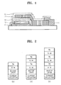
- FIG. 1 is a schematic diagram of a conventional thin film battery.
- a thin film battery is basically constructed such that a cathode 12, an electrolyte 14, an anode 13 and a protective layer 15 are sequentially stacked on a current collector 11 in forms of thin films, and the overall thickness of the layered structure is approximately 10 ⁇ m.
- the thus-constructed conventional thin film battery has the following advantages.
- the thin film battery is fabricated by depositing a cathode and an anode in forms of thin films, the battery can have a high current density. Also, since the cathode and the anode are formed in forms of thin films, the moving distance among ions is reduced to thus facilitate and promote ionic movement, thereby reducing the amounts of reactants. Since such thin film batteries can be easily manufactured in arbitrary shapes and sizes to be conformable to special purposes, they are very promising as main power sources for miniaturized electronic devices, micro-electromachanical systems (MEMS) and miniature sensor devices.
- MEMS micro-electromachanical systems
- a thin film battery is manufactured by the same method as that of a semiconductor device, it can be mounted on a semiconductor chip together with an electronic circuit, thereby implementing a complementary metal oxide semiconductor (CMOS) memory chip using the thin film battery as a back-up power source. Also, an unused area of an electronic device can be minimized, thereby increasing the space utilization efficiency of the electronic device to a maximum. Further, since thin film batteries operating at various voltages and capacities can be realized by serial and parallel connections of unit cells through appropriate designs and etching steps, they can be widely used in a variety of applications.
- CMOS complementary metal oxide semiconductor
- Thin films for an anode for such thin film batteries are typically lithium thin films formed by deposition of a lithium metal.
- the lithium metal has a low melting point of approximately 180°C and is melt due to heat generated during soldering in the course of packaging, resulting in damage of a device. Also, since the lithium metal is highly reactive in the air, its manageability is poor and a separate device for isolating the lithium metal from moisture and oxygen must be additionally installed. Thus, the use of a lithium metal has various problems to be widely put into practical use as an electrode material for power sources of super-miniaturized electronic devices.
- lithium alloys In order to overcome the low charging/discharging cycle efficiency of lithium, research into lithium alloys has been carried out. Much attention has been paid to metals capable of forming lithium alloys, such as tin (Sn), silicon (Si) or aluminum (Al), as promising next generation anode active materials. While these anode active materials have good capacity characteristics at low operating voltages in contrast with lithium, a volumetric change in active material, encountered by insertion and release of lithium during charging/discharging cycles, results in a poor thin film structure for an anode and impediment to cycle characteristics, thereby reducing charge/discharge capacity.
- metals capable of forming lithium alloys such as tin (Sn), silicon (Si) or aluminum (Al)
- a thin film for an anode of a lithium secondary battery includes a current collector and an anode active material layer formed on the current collector, wherein the anode active material layer is a multi-layered thin film formed by stacking a'silver (Ag) layer and a silicon-metal (Si-M) layer having silicon dispersed in a base made from metal reacting with silicon while not reacting with lithium.
- the anode active material layer is a multi-layered thin film formed by stacking a'silver (Ag) layer and a silicon-metal (Si-M) layer having silicon dispersed in a base made from metal reacting with silicon while not reacting with lithium.
- a method of preparing a thin film for an anode of a lithium secondary battery includes (a) forming a thin film of silicon-metal (Si-M) by depositing a metal reacting with silicon while not reacting with lithium and silicon on a current collector in forms of thin films, (b) forming a thin film of silver (Ag) by depositing Ag on the Si-M layer in form of a thin film, and (c) forming a multi-layered thin film by repeating the steps (a) and (b) one or more times.
- Si-M silicon-metal
- Si Silicon (Si) exhibits a large capacity relative to lithium (Li) at low operating voltages, and reacts with Li according to the following reaction scheme: Si + 4.4 Li ⁇ Li 4.4 Si
- Si has various advantages including a very high energy density of approximately 4000mAh/g, as charging/discharging cycles proceed, repetition of insertion/release of Li causes repeated expansion and contraction in volume of silicon particles, resulting in cracks. Thus, some silicon particles may not be electrically connected, thereby reducing charging/discharging capacity, making Si difficult to be used as an anode active material.
- the feature of the present invention lies in that Si and metal (M) are maintained at a bonded state during insertion of Li while suppressing the shortcoming of Si, that is, stress due to volumetric expansion of Si, thereby limiting Li-Si reactions, and the structural stability is increased, thereby improving a cycle characteristic.
- the metal in the Si-M layer has excellent ductility and toughness and has a strong chemical affinity to Si to react therewith while not reacting Li.
- the formation enthalpy between Si and metal added must have a negative value ( ⁇ H(Si-M) ⁇ 0). Also, the metal must be capable of maintaining a Si-M bond during insertion and release of Li.
- the metal include at least one selected from the group consisting of vanadium (V), manganese (Mn), titanium (Ti), nickel (Ni), platinum (Pt), zirconium (Zr), chromium (Cr), iron (Fe), hafnium (Hf), molybdenum (Mo), niobium (Nb), ruthenium (Ru) and tantalum (Ta).
- vanadium (V) has excellent ductility and toughness and a strong chemical affinity to Si, thereby suppressing Si-Li reactivity during insertion of Li and exhibiting the structural stability during repetition of insertion and release of Li.
- silver (Ag) acting as a medium through which Li ions and electrons can move is used to form an anode active material layer, as one of components of a multi-layered thin film for an anode with a Si-M layer. Since Ag does not react with Si, the capacity and reversibility of Li-Si reaction can be secured and the structural stability of an active material can be secured under the conditions of heat treatment that is required for a later packaging process of a thin film battery.
- charging/discharging cycles can vary by controlling micro structures, crystallinity, sizes and distribution features of substances used for the anode active material according to the thicknesses and arrangement order of Si-M and Ag layers, the overall thickness of the anode active material layer, heat treatment conditions of forming a thin film, mixture ratios of Si and M and so on.
- the metal (M) content (x) in the Si-M (Si (1-x) -M x ) layer as the anode active material layer is preferably in the range of 5 to 50 mol%, more preferably in the range of 20 to 30 mol%. If the amount of metal (M) relative to Si exceeds the above range, microparticles of Si as an active material reacting with Li are surrounded by M atoms, that is, Si is shielded by ambient metal, the excess gives rise to the disadvantage that Si atoms cannot react with Li, thereby reducing the electrode capacity as designed. Also, if the amount of metal (M) relative to Si is less than the above range, the shortage entails the disadvantage that Li-Si reactivity is increased, thereby exhibiting unappreciable effect in suppressing a change in the volume of Si particles.
- the topmost layer thereof is preferably made from Ag, which is because a good cycle characteristic of a lithium secondary battery employing the thin film for an anode can be achieved through such arrangement.
- FIGS. 2A through 2C a thin film for an anode according to an embodiment of the present invention will be described in more detail with reference to FIGS. 2A through 2C.
- the thin film for an anode according to the present invention includes a current collector and a multi-layered thin film consisting of an Si-M layer as an anode active material layer and a silver (Ag) layer stacked on the current collector.
- the anode current collector generally includes, but is not limited to, a copper (Cu) layer, and the thickness thereof is generally in the range of 100 ⁇ 300 nm.
- Cu copper
- the anode active material layer shown in FIG. 2A includes sequentially stacked Si-M/Ag layers.
- the anode active material layer shown in FIG. 2B includes sequentially stacked Si-M/Ag/Si-M/Ag layers.
- the anode active material layer shown in FIG. 2C includes sequentially stacked Si-M/Ag/Si-M/Ag/Si-M/Ag layers.
- the anode active material layer according to the present invention is a preferably structure in which the Si-M layer and the Ag layer are alternately stacked, more preferably a structure in which an Ag layer is interposed between Si-M layers, in view of the effect of suppressing an increase in the volume of the anode active material layer.
- Ag acts as a medium through which Li ions and electrons can move and does not react with Si, the capacity and reversibility of Li-Si reaction can be secured and the structural stability of an active material can be secured under the conditions of heat treatment that is required for a later packaging process of a thin film battery.
- the thickness of a Si-M layer and number of stacked layers, which are in proportion to the amount of an anode active material, can vary according to the requirements of a device and the capacity of a cathode.
- the preferred thickness of an Si-M layer is in the range of 50 to 450 ⁇ . If the thickness of an Si-M layer is less than 50 ⁇ , it is necessary to increase the number of stacked layers of Si-M/Ag to meet the requirement as designed. If the number of Ag layers exceeds a predetermined range, the overpotential of a thin film for an anode may undesirably increase. If thickness of an Si-M layer is greater than 450 ⁇ , the metal added cannot sufficiently suppress an increase in the volume of Si.
- Li-Ag alloy tends to react with Li at low voltages of 0.08 V or less to form a stable Li-Ag alloy.
- an Li-Ag alloy is slowly decomposed to Li and Ag so that the Li cannot completely escape from the Li-Ag alloy, from which low reversibility is resulted, acting as irreversible capacity.
- Ag is deposited to a minimum thickness, preferably in the range of 10 ⁇ 70 ⁇ . If the thickness of an Ag layer is less than 10 ⁇ , the effect of suppressing a change in the volume of an Si layer is unappreciable. If the thickness is greater than 70 ⁇ , the Li-Ag alloy is slowly decomposed to Li and Ag, which is disadvantageous.
- the multi-layered thin film consisting of Si-M layer/Ag layer stacked on a current collector according to the present invention makes it possible to achieve a lithium secondary battery having various performance characteristics according to the stacked order and thickness thereof.
- the Si-M layer is formed by dispersing Si on a base formed from metal which does not react with Li but reacts with Si through a thin film deposition process.
- Methods of forming the Si-M layer include, but are not limited to, co-sputtering, e-beam evaporation, ion-beam assisted deposition and chemical vapor deposition.
- the processing conditions of each method are not specially restricted, and explanations thereof will now be given briefly.
- a multi-component thin film can be manufactured by co-deposition including mosaic sputtering using a mosaic target, co-sputtering using two or more targets, or sputtering using an alloy target.
- thin films having various compositions can be obtained by adjusting the radio frequency (rf) power applied to the respective targets.
- the only parameter for adjustment of the composition of a thin film is the rf power applied to the respective targets because other deposition factors, including deposition pressure, gas flow rate, mixture ratio of gas and the like, are under the same conditions.
- the deposition power of a basic material i.e., Si
- the deposition powers of materials added are varied.
- the deposition power for Si is in the range of 100 to 300 W
- the deposition power for metal (M) is in the range of 0 to 100 W.
- the number of chips is a parameter for a compositional change, with other sputtering conditions maintained to be the same.
- co-sputtering of Si and metal selected from V, Mn, Ti, Ni, Pt, Zr, Cr, Fe, Hf, Mo, Nb, Ru and Ta a thin film of Si having a size of several tens of nanometers dispersed into the metal base is attained.
- characteristics of a finally obtained anode active material slightly vary according to distribution phase, particle size or mixture ratio of the metal dispersed in Si.
- a good cycle characteristic of the metal can be achieved by controlling the metal to be uniformly distributed in forms of microparticles in Si.
- e-beams are simultaneously focused onto different deposition sources for evaporation and co-sputtered on a substrate.
- argon ions may be accelerated to then be irradiated onto the substrate, thereby increasing the mobility of deposited atoms and changing the surface state of a thin film.
- the composition of the thin film can be changed by adjusting the flux (e-beam current) of e-beams applied to the respective deposition sources.
- the crystallinity and microstructure of the thin film can be adjusted by changing acceleration voltages.
- Deposition using ion-beam assisted deposition increases the mobility and reactivity of atoms as accelerated e-beams collide with atoms deposited on a substrate, thereby appropriately adjusting the conditions of ion-beams.
- amorphous, crystalline multi-component thin films can be manufactured.
- the composition of the thin film can be changed by adjusting ion-beam current of the ion-beams applied to the respective deposition sources.
- the crystallinity and microstructure of the thin film can be adjusted by changing the Ar ion flux and acceleration voltages.
- a buffering layer is preferably formed between a current collector and an anode active material layer.
- the buffering layer is formed of at least one metal selected from the group consisting of V, Ni, Mo and Cu, and serves to relieve the stress between the anode active material layer and the current collector and to secure the stability at the interface therebetween.
- the thickness of the buffering layer is preferably in the range of 50 to 250 ⁇ . If the thickness of the buffering layer is less than 50 ⁇ , the buffering layer cannot sufficiently perform a buffering action to relieve the stress the anode active material layer and the current collector. If the thickness of the buffering layer is greater than 250 ⁇ , the excess gives rise to an increase in the overall volume of the thin film for an anode without a considerable change in the electrochemical property, which is disadvantageous.
- Various components of a thin film that is, Si, V and Ag targets each having a diameter of 2 inches, were sequentially deposited on a copper (Cu) substrate to prepare a Cu/V (200 ⁇ )/Si-V (300 ⁇ )/Ag (50 ⁇ ) thin film for an anode.
- the initial degree of vacuum was first adjusted to 2 ⁇ 10 -6 torr or less, a vanadium (V) layer was then deposited to a thickness of 200 ⁇ at rf power of 50 W under the condition of Ar gas induced at 5 mTorr operating pressure and 10 sccm flow rate, and Si and V were co-sputtered on the resultant product to a thickness of 300 ⁇ to prepare a single-layered Si-V film (sometimes also called a "layer" throughout the specification). Ag was then deposited on the Si-V film to a thickness of 50 ⁇ .
- the rf power applied to the V target in the range of 0 to 100 W was varied, while fixing the rf power applied to the Si target to 200 W, thereby manufacturing thin films for an anode having various compositions.
- the thickness of the single-layered Si (1-x) -V x film was fixed to 300 ⁇ .
- a lithium secondary batteries were manufactured using Li metals as a counter electrode and a reference electrode and an electrolytic solution of 1M LiPF 6 dissolved in a mixed solvent of ethylene carbonate (EC) and diethyl carbonate (DEC).
- EC ethylene carbonate
- DEC diethyl carbonate
- a lithium secondary battery was manufactured by the same method as in Example 1, except that a Cu/ V(200 ⁇ )/Si(300 ⁇ ) thin film for an anode was manufactured by depositing only a 2-inch diameter Si target on a Cu current collector.
- V Vanadium (V) dependent cycle characteristics of the lithium secondary batteries employing the thin films for an anode prepared by Example 1 and Comparative Example 1 were evaluated, and the evaluation results are shown in FIG. 3.
- the amount of V added was 30 mol%, the thin film for an anode was not lower than 95% in initial capacity maintenance ratio even after 100 cycles.
- deterioration of an anode active material due to volumetric expansion and shrinkage of Si was considerably reduced such that V microparticles were distributed to surround Si particles by a co-sputtering method, thereby greatly improving cycle characteristics.
- Cycle characteristics of a multi-layered thin film for an anode having a composition of Si 0.7 V 0.3 /Ag (50 ⁇ ) depending on the thickness of a Si 0.7 V 0.3 layer were evaluated, and the evaluation results are shown in FIG. 4.
- Si and V were co-sputtered with rf powers of 200 W and 50 W, respectively, to manufacture a 100 to 450 ⁇ thick thin film for an anode having the above composition.
- Evaluation of cycle characteristics was made by repeating at least 150 cycles of charging and discharging at a constant current density of 50 ⁇ A/cm 2 within the potential range of 0 to 1.5 V.
- the thickness of the single-layered Si-V film having the above composition increased, the charge/discharge cycle efficiency was lowered.
- the thickness of the single-layered Si-V film was greater than or equal to 450 ⁇ , the capacity was sharply decreased according to an increase in the number of cycles.
- the thickness of the single-layered Si-V film was less than 450 ⁇ , cycle characteristics of the thin film for an anode were improved.
- the thin film was not lower than 90% in the initial capacity maintenance ratio even after 150 cycles.
- Thin films for an anode were manufactured in the same manner as in Example 1, except that each Si 0.7 M 0.3 layer (300 ⁇ ) was formed using Mn, Ti and Zr as metals (M) in an Si-M layer as anode active material layers, instead of V, respectively.
- FIGS. 6A through 6C show cycle characteristics thereof. Evaluation of cycle characteristics of these thin films for an anode was made by repeating at least 50 cycles of charging and discharging.
- FIGS. 6A through 6C in the case of single-layered films with Mn, Ti and Zr added, like in the case of the single-layered Si-V film, deterioration of anode active materials due to volumetric expansion and shrinkage of Si was considerably reduced, thereby greatly improving cycle characteristics compared to the case of Comparative Example 1.
- the initial discharge capacity of each single-layered film was maintained without a considerable reduction even after 90 cycles. This is because the metals added are strongly bonded to Si while being retained at amorphous structures during insertion and release of Li.
- a single-layered Si-Cu film was manufactured in the same manner as in Example 2 and cycle characteristics thereof were evaluated. The evaluation results are shown in FIG. 6D. Evaluation of cycle characteristics was made by repeating at least 200 cycles of charging and discharging at a constant current density of 50 ⁇ A/cm 2 within the potential range of 0 to 1.5 V. All metals added in Examples 2-4 have strong chemical affinity to Si and are capable of maintaining Si-M bonds during insertion and release of Li. As shown in FIG. 6D, in the case where the metal added was Cu, the capacity was considerably reduced within the period of approximately 20 cycles. Such a considerable reduction in the capacity is because Cu is not so strongly bonded to Si, compared to the above-referenced metals, resulting in cutting of a Si-Cu bond due to insertion of Li into the Si-Cu bond.
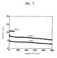
- Various components of a thin film for an anode that is, Si, V and Ag targets each having a diameter of 2 inches, were sequentially deposited on a Cu substrate to prepare thin films for an anode having the structures shown in Table 1.
- the initial degree of vacuum was first adjusted to 2 ⁇ 10 -6 torr or less, a vanadium (V) layer was then deposited to a thickness of 200 ⁇ at rf power of 50 W under the condition of Ar gas induced at 5 mTorr operating pressure and 10 sccm flow rate, and an Ag layer and an Si-V layer alternately deposited on the resultant product.
- the Ag layer was deposited between Si-V layers to a thickness of 50 ⁇ at a dc voltage of 270 V with a current of 30mA, and the Si-V layer having the same composition as in Example 1, that is, the Si 0.7 V 0.3 layer, was deposited to a thickness of 150 ⁇ .
- Sample Layered structure of anode active material MSB-1 Cu/V(200 ⁇ )/(Si-V)/Ag MSB-2 Cu/V(200 ⁇ )/(Si-V)/Ag/(Si-V)/Ag MSB-3 Cu/V(200 ⁇ )/(Si-V)/Ag/(Si-V)/Ag/(Si-V)/Ag/(Si-V)/Ag.
- Cycle characteristics of the multi-layered films are shown in FIG. 7.
- the cycle characteristics were evaluated by repeating at least 200 cycles of charging and discharging at a constant current density of 50 ⁇ A/cm 2 within the potential range of 0 to 1.5 V.
- the capacities of the multi-layered films increased in proportion to the number of Si-V layers. In cases of layered structures of a Si-V layer and two Si-V layers, a slight decrease in the capacity was observed within an initial period of several cycles, and 90% or higher of the initial capacity was maintained even after 200 cycles.
- the Ag layer is interposed between the Si-V layers, thereby increasing the capacity without deterioration in cycle characteristics even when the overall thickness of the Si-V layers is increased up to 450 ⁇ .
- the use of a multi-layered Si-V/Ag film as an anode active material layer makes it possible to design a thin film for an anode having a capacity larger than in the case of using a single-layered Si-V film.
- a lithium secondary thin film battery was manufactured using a single-layered Si-V film as follows. First, a platinum (Pt) film as a cathode collector was deposited on an alumina (Al 2 O 3 ) substrate to a thickness of 3000 ⁇ at rf power of 50 W under the condition of Ar gas induced at 5 mTorr operating pressure and 10 sccm flow rate, and then LiCoO 2 as a cathode material was deposited thereon to a thickness of 7000 ⁇ at rf power of 150 W in a mixed gas atmosphere of argon and oxygen (8:2 in sccm) induced at 5 mTorr operating pressure and 10 sccm flow rate.
- Cycle characteristics of the thus-manufactured thin film battery were evaluated within the potential range of 2 to 4.2 V with charge and discharge currents varied, and the evaluation results are shown in FIG. 8. As shown in FIG. 8, the thin film battery exhibits very stable cycle characteristics.
- the initial capacity 9.4 ⁇ Ah was sharply decreased to 8.0 ⁇ Ah during the second cycle.
- the battery capacity was gradually increased up to 9.0 ⁇ Ah until 20 cycles were repeated, and then a good cycle characteristic was exhibited afterwards without a considerable reduction in the capacity.
- the upper cut-off charge voltages were increased to 4.1 V and 4.2 V and the thin film battery was subjected to a cycling test. The result showed that the battery capacity increased but sharply decreased subsequently within the period of several cycles.
- the cycle characteristic of the thin film for an anode according to the present invention can be remarkably improved by suppressing volumetric expansion and shrinkage of Si during charging/discharging cycles. Therefore, use of the thin film for an anode according to the present invention can greatly improve the chemical, mechanical stability of the interface between an electrode and an electrolyte, thereby preparing a lithium secondary battery having improved life characteristics.
Landscapes
- Chemical & Material Sciences (AREA)
- Chemical Kinetics & Catalysis (AREA)
- Electrochemistry (AREA)
- General Chemical & Material Sciences (AREA)
- Engineering & Computer Science (AREA)
- Materials Engineering (AREA)
- Manufacturing & Machinery (AREA)
- Composite Materials (AREA)
- Inorganic Chemistry (AREA)
- Battery Electrode And Active Subsutance (AREA)
- Secondary Cells (AREA)
- Cell Electrode Carriers And Collectors (AREA)
Abstract
Description
| Sample | Layered structure of anode active material |
| MSB-1 | Cu/V(200 Å)/(Si-V)/Ag |
| MSB-2 | Cu/V(200 Å)/(Si-V)/Ag/(Si-V)/Ag |
| MSB-3 | Cu/V(200 Å)/(Si-V)/Ag/(Si-V)/Ag/(Si-V)/Ag |
Claims (11)
- A thin film for an anode of a lithium secondary having a current collector and an anode active material layer formed on the current collector, wherein the anode active material layer is a multi-layered thin film formed by stacking a silver (Ag) layer and a silicon-metal (Si-M) layer having silicon dispersed in a base made from metal reacting with silicon while not reacting with lithium.
- The thin film for an anode according to claim 1, wherein the metal (M) is at least one selected from the group consisting of vanadium (V), manganese (Mn), titanium (Ti), nickel (Ni), platinum (Pt), zirconium (Zr), chromium (Cr), iron (Fe), hafnium (Hf), molybdenum (Mo), niobium (Nb), ruthenium (Ru) and tantalum (Ta).
- The thin film for an anode according to claim 1 or 2, wherein the metal (M) content in the Si-M layer as the anode active material layer is in the range of 5 to 50 mol%, and preferably in the range of 20 to 30 mol%.
- The thin film for an anode according to any one of claims 1 to 3, wherein a buffering layer made from at least one metal selected from the group consisting of V, Ni, Mo and Cu is formed between the current collector and the anode active material layer.
- The thin film for an anode according to claim 4, wherein the thickness of the buffering layer is in the range of 50 to 250 Å.
- The thin film for an anode according to any one of claims 1 to 5, wherein the thickness of the Si-M layer is in the range of 50 to 450 Å and/or the thickness of the Ag layer is in the range of 10 to 70 Å.
- The thin film for an anode according to any one of claims 1 to 6, wherein the Si-M layer and the Ag layer are alternately formed and/or the Ag layer is disposed between Si-M layers and/or the topmost layer of the multi-layered thin film is made from Ag.
- A method of manufacturing a thin film for an anode of a lithium secondary battery comprising:(a) forming a thin film of silicon-metal (Si-M) by depositing a metal reacting with silicon while not reacting with lithium and silicon on a current collector in forms of thin films;(b) forming a thin film of silver (Ag) by depositing Ag on the Si-M layer in form of a thin film; and(c) forming a multi-layered thin film by repeating the steps (a) and (b) one or more times.
- The method according to claim 8, wherein the metal (M) is at least one selected from the group consisting of vanadium (V), manganese (Mn), titanium (Ti), nickel (Ni), platinum (Pt), zirconium (Zr), chromium (Cr), iron (Fe), hafnium (Hf), molybdenum (Mo), niobium (Nb), ruthenium (Ru) and tantalum (Ta).
- The method according to claim 8 or 9, wherein the metal (M) content in the Si-M layer as the anode active material layer is in the range of 5 to 50 mol%.
- The method according to any one of claims 8 to 10, wherein deposition in steps (a) and (b) is performed by a method selected from co-sputtering, e-beam evaporation and ion-beam assisted deposition.
Applications Claiming Priority (2)
| Application Number | Priority Date | Filing Date | Title |
|---|---|---|---|
| KR10-2001-0051588A KR100382767B1 (en) | 2001-08-25 | 2001-08-25 | Anode thin film for Lithium secondary battery and manufacturing method thereof |
| KR2001051588 | 2001-08-25 |
Publications (3)
| Publication Number | Publication Date |
|---|---|
| EP1289045A2 true EP1289045A2 (en) | 2003-03-05 |
| EP1289045A3 EP1289045A3 (en) | 2004-03-03 |
| EP1289045B1 EP1289045B1 (en) | 2006-03-15 |
Family
ID=36848433
Family Applications (1)
| Application Number | Title | Priority Date | Filing Date |
|---|---|---|---|
| EP02007548A Expired - Lifetime EP1289045B1 (en) | 2001-08-25 | 2002-04-03 | Thin film for anode of lithium secondary battery and manufacturing method thereof |
Country Status (5)
| Country | Link |
|---|---|
| US (2) | US6824922B2 (en) |
| EP (1) | EP1289045B1 (en) |
| JP (1) | JP3619817B2 (en) |
| KR (1) | KR100382767B1 (en) |
| DE (1) | DE60209827T2 (en) |
Cited By (3)
| Publication number | Priority date | Publication date | Assignee | Title |
|---|---|---|---|---|
| US7816032B2 (en) | 2003-11-28 | 2010-10-19 | Panasonic Corporation | Energy device and method for producing the same |
| EP1873846A4 (en) * | 2005-03-23 | 2013-04-03 | Pionics Co Ltd | Negative electrode active material particle for lithium secondary battery, negative electrode and methods for producing those |
| EP4322250A4 (en) * | 2021-12-22 | 2025-07-16 | Lg Energy Solution Ltd | Prelithiation process for negative electrode for lithium secondary battery, negative electrode for lithium secondary battery and lithium secondary battery with negative electrode |
Families Citing this family (82)
| Publication number | Priority date | Publication date | Assignee | Title |
|---|---|---|---|---|
| KR100487021B1 (en) * | 2002-06-07 | 2005-05-03 | 백홍구 | Negative electrode for lithium secondary thin battery and manufacturing method thereof |
| US7993773B2 (en) | 2002-08-09 | 2011-08-09 | Infinite Power Solutions, Inc. | Electrochemical apparatus with barrier layer protected substrate |
| US8445130B2 (en) | 2002-08-09 | 2013-05-21 | Infinite Power Solutions, Inc. | Hybrid thin-film battery |
| US8431264B2 (en) | 2002-08-09 | 2013-04-30 | Infinite Power Solutions, Inc. | Hybrid thin-film battery |
| US8236443B2 (en) | 2002-08-09 | 2012-08-07 | Infinite Power Solutions, Inc. | Metal film encapsulation |
| US8021778B2 (en) | 2002-08-09 | 2011-09-20 | Infinite Power Solutions, Inc. | Electrochemical apparatus with barrier layer protected substrate |
| US8404376B2 (en) | 2002-08-09 | 2013-03-26 | Infinite Power Solutions, Inc. | Metal film encapsulation |
| US20070264564A1 (en) * | 2006-03-16 | 2007-11-15 | Infinite Power Solutions, Inc. | Thin film battery on an integrated circuit or circuit board and method thereof |
| US8394522B2 (en) | 2002-08-09 | 2013-03-12 | Infinite Power Solutions, Inc. | Robust metal film encapsulation |
| JP3755502B2 (en) * | 2002-09-11 | 2006-03-15 | ソニー株式会社 | Non-aqueous electrolyte battery |
| GB2395059B (en) | 2002-11-05 | 2005-03-16 | Imp College Innovations Ltd | Structured silicon anode |
| US8728285B2 (en) | 2003-05-23 | 2014-05-20 | Demaray, Llc | Transparent conductive oxides |
| JP4374491B2 (en) * | 2003-10-21 | 2009-12-02 | 株式会社大和化成研究所 | Negative electrode for lithium secondary battery |
| JP5089276B2 (en) * | 2003-11-28 | 2012-12-05 | パナソニック株式会社 | Energy device and manufacturing method thereof |
| US7968233B2 (en) * | 2004-02-18 | 2011-06-28 | Solicore, Inc. | Lithium inks and electrodes and batteries made therefrom |
| WO2005117169A1 (en) * | 2004-05-27 | 2005-12-08 | Matsushita Electric Industrial Co., Ltd. | Wound nonaqueous secondary battery and electrode plate used therein |
| FR2873496B1 (en) * | 2004-07-26 | 2016-04-01 | Commissariat Energie Atomique | ELECTRODE FOR LITHIUM ACCUMULATOR, METHOD OF MANUFACTURING SUCH ELECTRODE AND LITHIUM ACCUMULATOR COMPRISING SUCH ELECTRODE |
| KR100566592B1 (en) * | 2004-09-16 | 2006-03-31 | 주식회사 디지털텍 | Anode Thin Film for Lithium Ion Polymer Battery and Manufacturing Method Thereof |
| JP5103903B2 (en) * | 2004-09-22 | 2012-12-19 | ソニー株式会社 | Secondary battery electrolyte and secondary battery |
| US7959769B2 (en) | 2004-12-08 | 2011-06-14 | Infinite Power Solutions, Inc. | Deposition of LiCoO2 |
| KR101127370B1 (en) | 2004-12-08 | 2012-03-29 | 인피니트 파워 솔루션스, 인크. | Deposition of licoo2 |
| KR100734060B1 (en) * | 2005-06-24 | 2007-07-02 | 건국대학교 산학협력단 | LLT SOLID ELECTROLYTE WITH LiPON PROTECTIVE LAYER, AND MANUFACTURING METHOD THEREOF |
| KR100684733B1 (en) | 2005-07-07 | 2007-02-20 | 삼성에스디아이 주식회사 | Lithium secondary battery |
| JP4849307B2 (en) * | 2005-09-29 | 2012-01-11 | ソニー株式会社 | Negative electrode and battery |
| EP1955393B1 (en) * | 2005-12-01 | 2014-08-27 | 3M Innovative Properties Company | Electrode compositions based on an amorphous alloy having a high silicon content |
| KR100763892B1 (en) * | 2006-01-20 | 2007-10-05 | 삼성에스디아이 주식회사 | Anode active material, manufacturing method thereof, and anode and lithium battery using same |
| GB0601319D0 (en) | 2006-01-23 | 2006-03-01 | Imp Innovations Ltd | A method of fabricating pillars composed of silicon-based material |
| GB0601318D0 (en) | 2006-01-23 | 2006-03-01 | Imp Innovations Ltd | Method of etching a silicon-based material |
| CA2535064A1 (en) * | 2006-02-01 | 2007-08-01 | Hydro Quebec | Multi-layer material, production and use thereof as an electrode |
| CN101523571A (en) | 2006-09-29 | 2009-09-02 | 无穷动力解决方案股份有限公司 | Masking and material confinement of a battery layer deposited on a flexible substrate |
| US8197781B2 (en) | 2006-11-07 | 2012-06-12 | Infinite Power Solutions, Inc. | Sputtering target of Li3PO4 and method for producing same |
| GB0709165D0 (en) | 2007-05-11 | 2007-06-20 | Nexeon Ltd | A silicon anode for a rechargeable battery |
| GB0713896D0 (en) | 2007-07-17 | 2007-08-29 | Nexeon Ltd | Method |
| GB0713895D0 (en) | 2007-07-17 | 2007-08-29 | Nexeon Ltd | Production |
| GB0713898D0 (en) | 2007-07-17 | 2007-08-29 | Nexeon Ltd | A method of fabricating structured particles composed of silcon or a silicon-based material and their use in lithium rechargeable batteries |
| JP5169156B2 (en) | 2007-11-09 | 2013-03-27 | パナソニック株式会社 | Electrodes for electrochemical devices |
| CN101903560B (en) | 2007-12-21 | 2014-08-06 | 无穷动力解决方案股份有限公司 | Method for sputter targets for electrolyte films |
| US8268488B2 (en) | 2007-12-21 | 2012-09-18 | Infinite Power Solutions, Inc. | Thin film electrolyte for thin film batteries |
| US8518581B2 (en) | 2008-01-11 | 2013-08-27 | Inifinite Power Solutions, Inc. | Thin film encapsulation for thin film batteries and other devices |
| WO2009124191A2 (en) | 2008-04-02 | 2009-10-08 | Infinite Power Solutions, Inc. | Passive over/under voltage control and protection for energy storage devices associated with energy harvesting |
| JP2012500610A (en) | 2008-08-11 | 2012-01-05 | インフィニット パワー ソリューションズ, インコーポレイテッド | Energy device with integrated collector surface and method for electromagnetic energy acquisition |
| CN102150185B (en) | 2008-09-12 | 2014-05-28 | 无穷动力解决方案股份有限公司 | Energy device with integral conductive surface for data communication via electromagnetic energy and method thereof |
| WO2010042594A1 (en) | 2008-10-08 | 2010-04-15 | Infinite Power Solutions, Inc. | Environmentally-powered wireless sensor module |
| GB2464157B (en) | 2008-10-10 | 2010-09-01 | Nexeon Ltd | A method of fabricating structured particles composed of silicon or a silicon-based material |
| GB2464158B (en) | 2008-10-10 | 2011-04-20 | Nexeon Ltd | A method of fabricating structured particles composed of silicon or a silicon-based material and their use in lithium rechargeable batteries |
| GB2470056B (en) | 2009-05-07 | 2013-09-11 | Nexeon Ltd | A method of making silicon anode material for rechargeable cells |
| JP5479775B2 (en) * | 2009-05-08 | 2014-04-23 | 古河電気工業株式会社 | Negative electrode for lithium ion secondary battery and method for producing the same |
| GB2470190B (en) | 2009-05-11 | 2011-07-13 | Nexeon Ltd | A binder for lithium ion rechargeable battery cells |
| US9853292B2 (en) | 2009-05-11 | 2017-12-26 | Nexeon Limited | Electrode composition for a secondary battery cell |
| CN102439778B (en) * | 2009-05-20 | 2016-02-10 | 萨普拉斯特研究有限责任公司 | For electrochemical device to be integrated within fixation means or on method |
| CN102576828B (en) | 2009-09-01 | 2016-04-20 | 萨普拉斯特研究有限责任公司 | Printed circuit board with integrated thin-film battery |
| KR101154545B1 (en) * | 2009-11-23 | 2012-06-13 | 지에스나노텍 주식회사 | Thin film battery hving improved efficiency of collecting electric current |
| GB201005979D0 (en) | 2010-04-09 | 2010-05-26 | Nexeon Ltd | A method of fabricating structured particles composed of silicon or a silicon-based material and their use in lithium rechargeable batteries |
| EP2577777B1 (en) | 2010-06-07 | 2016-12-28 | Sapurast Research LLC | Rechargeable, high-density electrochemical device |
| GB201009519D0 (en) | 2010-06-07 | 2010-07-21 | Nexeon Ltd | An additive for lithium ion rechargeable battery cells |
| GB201014706D0 (en) | 2010-09-03 | 2010-10-20 | Nexeon Ltd | Porous electroactive material |
| GB201014707D0 (en) | 2010-09-03 | 2010-10-20 | Nexeon Ltd | Electroactive material |
| US9705124B2 (en) | 2012-02-27 | 2017-07-11 | The Johns Hopkins University | High energy density Li-ion battery electrode materials and cells |
| US9478797B2 (en) * | 2013-01-25 | 2016-10-25 | Applejack 199 L.P. | System, method and apparatus for forming a thin film lithium ion battery |
| KR20140108380A (en) * | 2013-02-25 | 2014-09-11 | 엠케이전자 주식회사 | Secondary battery including silicon-metal alloy-based negative active material |
| US9537154B2 (en) | 2013-11-27 | 2017-01-03 | Lg Chem, Ltd. | Anode for secondary battery and secondary battery having the same |
| US10110036B2 (en) | 2016-12-15 | 2018-10-23 | StoreDot Ltd. | Supercapacitor-emulating fast-charging batteries and devices |
| US10549650B2 (en) | 2014-04-08 | 2020-02-04 | StoreDot Ltd. | Internally adjustable modular single battery systems for power systems |
| US10293704B2 (en) | 2014-04-08 | 2019-05-21 | StoreDot Ltd. | Electric vehicles with adaptive fast-charging, utilizing supercapacitor-emulating batteries |
| US11128152B2 (en) | 2014-04-08 | 2021-09-21 | StoreDot Ltd. | Systems and methods for adaptive fast-charging for mobile devices and devices having sporadic power-source connection |
| US10199646B2 (en) | 2014-07-30 | 2019-02-05 | StoreDot Ltd. | Anodes for lithium-ion devices |
| US10367192B2 (en) | 2016-04-07 | 2019-07-30 | StoreDot Ltd. | Aluminum anode active material |
| US10355271B2 (en) | 2016-04-07 | 2019-07-16 | StoreDot Ltd. | Lithium borates and phosphates coatings |
| US10818919B2 (en) | 2016-04-07 | 2020-10-27 | StoreDot Ltd. | Polymer coatings and anode material pre-lithiation |
| US11205796B2 (en) | 2016-04-07 | 2021-12-21 | StoreDot Ltd. | Electrolyte additives in lithium-ion batteries |
| US10916811B2 (en) | 2016-04-07 | 2021-02-09 | StoreDot Ltd. | Semi-solid electrolytes with flexible particle coatings |
| US10199677B2 (en) | 2016-04-07 | 2019-02-05 | StoreDot Ltd. | Electrolytes for lithium ion batteries |
| US10680289B2 (en) | 2016-04-07 | 2020-06-09 | StoreDot Ltd. | Buffering zone for preventing lithium metallization on the anode of lithium ion batteries |
| US10454101B2 (en) | 2017-01-25 | 2019-10-22 | StoreDot Ltd. | Composite anode material made of core-shell particles |
| US10290864B2 (en) | 2016-04-07 | 2019-05-14 | StoreDot Ltd. | Coated pre-lithiated anode material particles and cross-linked polymer coatings |
| US10367191B2 (en) | 2016-04-07 | 2019-07-30 | StoreDot Ltd. | Tin silicon anode active material |
| US10096859B2 (en) | 2016-04-07 | 2018-10-09 | StoreDot Ltd. | Electrolytes with ionic liquid additives for lithium ion batteries |
| RU175681U1 (en) * | 2017-08-08 | 2017-12-14 | Российская Федерация, от имени которой выступает Федеральное государственное казенное учреждение "Войсковая часть 68240" | NEGATIVE LITHIUM-ION BATTERY ELECTRODE BASED ON SILICON-CARBON COMPOSITE FILM |
| US12155068B2 (en) * | 2017-10-16 | 2024-11-26 | The Regents Of The University Of Colorado, A Body Corporate | Anode material—method of production and solid-state battery made therewith |
| US10608463B1 (en) | 2019-01-23 | 2020-03-31 | StoreDot Ltd. | Direct charging of battery cell stacks |
| US11831012B2 (en) | 2019-04-25 | 2023-11-28 | StoreDot Ltd. | Passivated silicon-based anode material particles |
| CN114207872A (en) * | 2019-08-09 | 2022-03-18 | 株式会社半导体能源研究所 | Negative electrode, secondary battery, and solid-state secondary battery |
Family Cites Families (11)
| Publication number | Priority date | Publication date | Assignee | Title |
|---|---|---|---|---|
| EP0690517B1 (en) * | 1994-05-30 | 2003-10-01 | Canon Kabushiki Kaisha | Rechargeable lithium battery |
| US6432585B1 (en) * | 1997-01-28 | 2002-08-13 | Canon Kabushiki Kaisha | Electrode structural body, rechargeable battery provided with said electrode structural body, and rechargeable battery |
| US6235427B1 (en) * | 1998-05-13 | 2001-05-22 | Fuji Photo Film Co., Ltd. | Nonaqueous secondary battery containing silicic material |
| KR100274892B1 (en) * | 1998-05-13 | 2001-02-01 | 김순택 | Lithium secondary battery |
| EP1028476A4 (en) * | 1998-09-08 | 2007-11-28 | Sumitomo Metal Ind | NEGATIVE ELECTRODE MATERIAL FOR NONAQUEOUS ELECTRODE SECONDARY ACCUMULATOR AND PROCESS FOR PRODUCTION THEREOF |
| PT1033767E (en) * | 1998-09-18 | 2010-07-13 | Canon Kk | Electrode material for negative pole of lithium secondary cell, electrode structure using said electrode material, lithium secondary cell using said electrode structure, and method for manufacturing said electrode structure and said lithium secondary |
| JP2000228187A (en) * | 1999-02-08 | 2000-08-15 | Wilson Greatbatch Ltd | Chemically deposited electrode component and its manufacture |
| JP2001006681A (en) * | 1999-06-16 | 2001-01-12 | Toyota Central Res & Dev Lab Inc | Negative electrode active material for lithium secondary battery and method for producing the same |
| US6699336B2 (en) * | 2000-01-13 | 2004-03-02 | 3M Innovative Properties Company | Amorphous electrode compositions |
| US6686090B2 (en) * | 2000-03-15 | 2004-02-03 | Kabushiki Kaisha Toshiba | Battery with a nonaqueous electrolyte and a negative electrode having a negative electrode active material occluding and releasing an active material |
| EP1207566B8 (en) * | 2000-11-18 | 2007-09-12 | Samsung SDI Co., Ltd. | Anode thin film for lithium secondary battery |
-
2001
- 2001-08-25 KR KR10-2001-0051588A patent/KR100382767B1/en not_active Expired - Fee Related
-
2002
- 2002-04-03 DE DE60209827T patent/DE60209827T2/en not_active Expired - Lifetime
- 2002-04-03 EP EP02007548A patent/EP1289045B1/en not_active Expired - Lifetime
- 2002-04-09 US US10/118,030 patent/US6824922B2/en not_active Expired - Lifetime
- 2002-08-20 JP JP2002239309A patent/JP3619817B2/en not_active Expired - Fee Related
-
2004
- 2004-11-29 US US10/997,882 patent/US7316867B2/en not_active Expired - Lifetime
Cited By (3)
| Publication number | Priority date | Publication date | Assignee | Title |
|---|---|---|---|---|
| US7816032B2 (en) | 2003-11-28 | 2010-10-19 | Panasonic Corporation | Energy device and method for producing the same |
| EP1873846A4 (en) * | 2005-03-23 | 2013-04-03 | Pionics Co Ltd | Negative electrode active material particle for lithium secondary battery, negative electrode and methods for producing those |
| EP4322250A4 (en) * | 2021-12-22 | 2025-07-16 | Lg Energy Solution Ltd | Prelithiation process for negative electrode for lithium secondary battery, negative electrode for lithium secondary battery and lithium secondary battery with negative electrode |
Also Published As
| Publication number | Publication date |
|---|---|
| US20030039889A1 (en) | 2003-02-27 |
| DE60209827D1 (en) | 2006-05-11 |
| US6824922B2 (en) | 2004-11-30 |
| JP3619817B2 (en) | 2005-02-16 |
| KR100382767B1 (en) | 2003-05-09 |
| EP1289045B1 (en) | 2006-03-15 |
| EP1289045A3 (en) | 2004-03-03 |
| US7316867B2 (en) | 2008-01-08 |
| US20050074673A1 (en) | 2005-04-07 |
| JP2003115294A (en) | 2003-04-18 |
| DE60209827T2 (en) | 2006-09-07 |
| KR20030017944A (en) | 2003-03-04 |
Similar Documents
| Publication | Publication Date | Title |
|---|---|---|
| US7316867B2 (en) | Method for manufacturing a multi-layered thin film for use as an anode in a lithium secondary battery | |
| EP1207566B1 (en) | Anode thin film for lithium secondary battery | |
| JP4846901B2 (en) | Electrode material and composition containing the same | |
| CN100555733C (en) | Battery | |
| US6168884B1 (en) | Battery with an in-situ activation plated lithium anode | |
| US7160646B2 (en) | Electrode for lithium secondary battery and lithium secondary battery | |
| KR100389908B1 (en) | Anode thin film for Lithium secondary battery | |
| US20020187399A1 (en) | Thin lithium film battery | |
| WO2006138362A2 (en) | Electrochemical apparatus with barrier layer protected substrate | |
| JP2003077529A (en) | Lithium battery and lithium secondary battery | |
| WO2005076389A9 (en) | Self-contained, alloy type, thin film anodes for lithium-ion batteries | |
| US20210351411A1 (en) | Secondary battery and method of preparing the same | |
| EP1289033B1 (en) | Anode thin film for lithium secondary battery and preparation method thereof | |
| KR20060124978A (en) | Thin Film Battery and Manufacturing Method Thereof | |
| KR100563081B1 (en) | Anode Thin Film for Lithium Secondary Battery and Manufacturing Method Thereof | |
| JPWO2005008809A1 (en) | Anode for non-aqueous electrolyte secondary battery and non-aqueous electrolyte secondary battery | |
| US7524585B2 (en) | Anode and battery using it | |
| KR100487021B1 (en) | Negative electrode for lithium secondary thin battery and manufacturing method thereof | |
| WO2024137066A2 (en) | Anode assembly for a battery cell |
Legal Events
| Date | Code | Title | Description |
|---|---|---|---|
| PUAI | Public reference made under article 153(3) epc to a published international application that has entered the european phase |
Free format text: ORIGINAL CODE: 0009012 |
|
| AK | Designated contracting states |
Kind code of ref document: A2 Designated state(s): AT BE CH CY DE DK ES FI FR GB GR IE IT LI LU MC NL PT SE TR Designated state(s): AT BE CH CY DE DK ES FI FR GB GR IE IT LI LU MC NL PT SE TR |
|
| AX | Request for extension of the european patent |
Extension state: AL LT LV MK RO SI |
|
| PUAL | Search report despatched |
Free format text: ORIGINAL CODE: 0009013 |
|
| AK | Designated contracting states |
Kind code of ref document: A3 Designated state(s): AT BE CH CY DE DK ES FI FR GB GR IE IT LI LU MC NL PT SE TR |
|
| AX | Request for extension of the european patent |
Extension state: AL LT LV MK RO SI |
|
| RIC1 | Information provided on ipc code assigned before grant |
Ipc: 7H 01M 10/40 B Ipc: 7H 01M 4/02 A Ipc: 7H 01M 4/38 B |
|
| 17P | Request for examination filed |
Effective date: 20040817 |
|
| AKX | Designation fees paid |
Designated state(s): DE FR GB |
|
| 17Q | First examination report despatched |
Effective date: 20041118 |
|
| GRAP | Despatch of communication of intention to grant a patent |
Free format text: ORIGINAL CODE: EPIDOSNIGR1 |
|
| GRAS | Grant fee paid |
Free format text: ORIGINAL CODE: EPIDOSNIGR3 |
|
| GRAA | (expected) grant |
Free format text: ORIGINAL CODE: 0009210 |
|
| AK | Designated contracting states |
Kind code of ref document: B1 Designated state(s): DE FR GB |
|
| REG | Reference to a national code |
Ref country code: GB Ref legal event code: FG4D |
|
| REF | Corresponds to: |
Ref document number: 60209827 Country of ref document: DE Date of ref document: 20060511 Kind code of ref document: P |
|
| ET | Fr: translation filed | ||
| PLBE | No opposition filed within time limit |
Free format text: ORIGINAL CODE: 0009261 |
|
| STAA | Information on the status of an ep patent application or granted ep patent |
Free format text: STATUS: NO OPPOSITION FILED WITHIN TIME LIMIT |
|
| 26N | No opposition filed |
Effective date: 20061218 |
|
| REG | Reference to a national code |
Ref country code: FR Ref legal event code: PLFP Year of fee payment: 15 |
|
| REG | Reference to a national code |
Ref country code: FR Ref legal event code: PLFP Year of fee payment: 16 |
|
| REG | Reference to a national code |
Ref country code: FR Ref legal event code: PLFP Year of fee payment: 17 |
|
| PGFP | Annual fee paid to national office [announced via postgrant information from national office to epo] |
Ref country code: GB Payment date: 20200325 Year of fee payment: 19 |
|
| PGFP | Annual fee paid to national office [announced via postgrant information from national office to epo] |
Ref country code: FR Payment date: 20200312 Year of fee payment: 19 |
|
| PGFP | Annual fee paid to national office [announced via postgrant information from national office to epo] |
Ref country code: DE Payment date: 20200325 Year of fee payment: 19 |
|
| REG | Reference to a national code |
Ref country code: DE Ref legal event code: R119 Ref document number: 60209827 Country of ref document: DE |
|
| GBPC | Gb: european patent ceased through non-payment of renewal fee |
Effective date: 20210403 |
|
| PG25 | Lapsed in a contracting state [announced via postgrant information from national office to epo] |
Ref country code: FR Free format text: LAPSE BECAUSE OF NON-PAYMENT OF DUE FEES Effective date: 20210430 Ref country code: GB Free format text: LAPSE BECAUSE OF NON-PAYMENT OF DUE FEES Effective date: 20210403 Ref country code: DE Free format text: LAPSE BECAUSE OF NON-PAYMENT OF DUE FEES Effective date: 20211103 |