EP1288905A2 - Current generating circuit, semiconductor integrated circuit, electro-optical device, and electronic apparatus - Google Patents
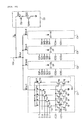
Current generating circuit, semiconductor integrated circuit, electro-optical device, and electronic apparatus Download PDFInfo
- Publication number
- EP1288905A2 EP1288905A2 EP02255886A EP02255886A EP1288905A2 EP 1288905 A2 EP1288905 A2 EP 1288905A2 EP 02255886 A EP02255886 A EP 02255886A EP 02255886 A EP02255886 A EP 02255886A EP 1288905 A2 EP1288905 A2 EP 1288905A2
- Authority
- EP
- European Patent Office
- Prior art keywords
- circuit
- current
- electro
- sub
- currents
- Prior art date
- Legal status (The legal status is an assumption and is not a legal conclusion. Google has not performed a legal analysis and makes no representation as to the accuracy of the status listed.)
- Ceased
Links
- 239000004065 semiconductor Substances 0.000 title claims 2
- 238000005401 electroluminescence Methods 0.000 claims description 4
- 230000005669 field effect Effects 0.000 claims description 3
- 238000010586 diagram Methods 0.000 description 13
- 238000006243 chemical reaction Methods 0.000 description 11
- 101150096622 Smr2 gene Proteins 0.000 description 7
- 239000004973 liquid crystal related substance Substances 0.000 description 7
- 230000001413 cellular effect Effects 0.000 description 5
- 230000006870 function Effects 0.000 description 4
- 230000003287 optical effect Effects 0.000 description 3
- 230000004044 response Effects 0.000 description 3
- BQCADISMDOOEFD-UHFFFAOYSA-N Silver Chemical compound [Ag] BQCADISMDOOEFD-UHFFFAOYSA-N 0.000 description 1
- 230000005540 biological transmission Effects 0.000 description 1
- 230000008859 change Effects 0.000 description 1
- 238000004891 communication Methods 0.000 description 1
- 230000003247 decreasing effect Effects 0.000 description 1
- 239000010408 film Substances 0.000 description 1
- 238000004020 luminiscence type Methods 0.000 description 1
- 238000000034 method Methods 0.000 description 1
- 238000012986 modification Methods 0.000 description 1
- 230000004048 modification Effects 0.000 description 1
- 230000003071 parasitic effect Effects 0.000 description 1
- 230000008569 process Effects 0.000 description 1
- 229910052709 silver Inorganic materials 0.000 description 1
- 239000004332 silver Substances 0.000 description 1
- 239000010409 thin film Substances 0.000 description 1
- 230000000007 visual effect Effects 0.000 description 1
Images









Classifications
-
- G—PHYSICS
- G09—EDUCATION; CRYPTOGRAPHY; DISPLAY; ADVERTISING; SEALS
- G09G—ARRANGEMENTS OR CIRCUITS FOR CONTROL OF INDICATING DEVICES USING STATIC MEANS TO PRESENT VARIABLE INFORMATION
- G09G3/00—Control arrangements or circuits, of interest only in connection with visual indicators other than cathode-ray tubes
- G09G3/20—Control arrangements or circuits, of interest only in connection with visual indicators other than cathode-ray tubes for presentation of an assembly of a number of characters, e.g. a page, by composing the assembly by combination of individual elements arranged in a matrix no fixed position being assigned to or needed to be assigned to the individual characters or partial characters
- G09G3/22—Control arrangements or circuits, of interest only in connection with visual indicators other than cathode-ray tubes for presentation of an assembly of a number of characters, e.g. a page, by composing the assembly by combination of individual elements arranged in a matrix no fixed position being assigned to or needed to be assigned to the individual characters or partial characters using controlled light sources
- G09G3/30—Control arrangements or circuits, of interest only in connection with visual indicators other than cathode-ray tubes for presentation of an assembly of a number of characters, e.g. a page, by composing the assembly by combination of individual elements arranged in a matrix no fixed position being assigned to or needed to be assigned to the individual characters or partial characters using controlled light sources using electroluminescent panels
- G09G3/32—Control arrangements or circuits, of interest only in connection with visual indicators other than cathode-ray tubes for presentation of an assembly of a number of characters, e.g. a page, by composing the assembly by combination of individual elements arranged in a matrix no fixed position being assigned to or needed to be assigned to the individual characters or partial characters using controlled light sources using electroluminescent panels semiconductive, e.g. using light-emitting diodes [LED]
- G09G3/3208—Control arrangements or circuits, of interest only in connection with visual indicators other than cathode-ray tubes for presentation of an assembly of a number of characters, e.g. a page, by composing the assembly by combination of individual elements arranged in a matrix no fixed position being assigned to or needed to be assigned to the individual characters or partial characters using controlled light sources using electroluminescent panels semiconductive, e.g. using light-emitting diodes [LED] organic, e.g. using organic light-emitting diodes [OLED]
- G09G3/3275—Details of drivers for data electrodes
-
- G—PHYSICS
- G09—EDUCATION; CRYPTOGRAPHY; DISPLAY; ADVERTISING; SEALS
- G09G—ARRANGEMENTS OR CIRCUITS FOR CONTROL OF INDICATING DEVICES USING STATIC MEANS TO PRESENT VARIABLE INFORMATION
- G09G3/00—Control arrangements or circuits, of interest only in connection with visual indicators other than cathode-ray tubes
- G09G3/20—Control arrangements or circuits, of interest only in connection with visual indicators other than cathode-ray tubes for presentation of an assembly of a number of characters, e.g. a page, by composing the assembly by combination of individual elements arranged in a matrix no fixed position being assigned to or needed to be assigned to the individual characters or partial characters
- G09G3/22—Control arrangements or circuits, of interest only in connection with visual indicators other than cathode-ray tubes for presentation of an assembly of a number of characters, e.g. a page, by composing the assembly by combination of individual elements arranged in a matrix no fixed position being assigned to or needed to be assigned to the individual characters or partial characters using controlled light sources
- G09G3/30—Control arrangements or circuits, of interest only in connection with visual indicators other than cathode-ray tubes for presentation of an assembly of a number of characters, e.g. a page, by composing the assembly by combination of individual elements arranged in a matrix no fixed position being assigned to or needed to be assigned to the individual characters or partial characters using controlled light sources using electroluminescent panels
-
- G—PHYSICS
- G09—EDUCATION; CRYPTOGRAPHY; DISPLAY; ADVERTISING; SEALS
- G09G—ARRANGEMENTS OR CIRCUITS FOR CONTROL OF INDICATING DEVICES USING STATIC MEANS TO PRESENT VARIABLE INFORMATION
- G09G2300/00—Aspects of the constitution of display devices
- G09G2300/08—Active matrix structure, i.e. with use of active elements, inclusive of non-linear two terminal elements, in the pixels together with light emitting or modulating elements
- G09G2300/0809—Several active elements per pixel in active matrix panels
- G09G2300/0842—Several active elements per pixel in active matrix panels forming a memory circuit, e.g. a dynamic memory with one capacitor
-
- G—PHYSICS
- G09—EDUCATION; CRYPTOGRAPHY; DISPLAY; ADVERTISING; SEALS
- G09G—ARRANGEMENTS OR CIRCUITS FOR CONTROL OF INDICATING DEVICES USING STATIC MEANS TO PRESENT VARIABLE INFORMATION
- G09G2310/00—Command of the display device
- G09G2310/02—Addressing, scanning or driving the display screen or processing steps related thereto
- G09G2310/0264—Details of driving circuits
- G09G2310/027—Details of drivers for data electrodes, the drivers handling digital grey scale data, e.g. use of D/A converters
-
- G—PHYSICS
- G09—EDUCATION; CRYPTOGRAPHY; DISPLAY; ADVERTISING; SEALS
- G09G—ARRANGEMENTS OR CIRCUITS FOR CONTROL OF INDICATING DEVICES USING STATIC MEANS TO PRESENT VARIABLE INFORMATION
- G09G2320/00—Control of display operating conditions
- G09G2320/02—Improving the quality of display appearance
- G09G2320/0271—Adjustment of the gradation levels within the range of the gradation scale, e.g. by redistribution or clipping
- G09G2320/0276—Adjustment of the gradation levels within the range of the gradation scale, e.g. by redistribution or clipping for the purpose of adaptation to the characteristics of a display device, i.e. gamma correction
-
- G—PHYSICS
- G09—EDUCATION; CRYPTOGRAPHY; DISPLAY; ADVERTISING; SEALS
- G09G—ARRANGEMENTS OR CIRCUITS FOR CONTROL OF INDICATING DEVICES USING STATIC MEANS TO PRESENT VARIABLE INFORMATION
- G09G2340/00—Aspects of display data processing
- G09G2340/04—Changes in size, position or resolution of an image
- G09G2340/0407—Resolution change, inclusive of the use of different resolutions for different screen areas
- G09G2340/0428—Gradation resolution change
-
- G—PHYSICS
- G09—EDUCATION; CRYPTOGRAPHY; DISPLAY; ADVERTISING; SEALS
- G09G—ARRANGEMENTS OR CIRCUITS FOR CONTROL OF INDICATING DEVICES USING STATIC MEANS TO PRESENT VARIABLE INFORMATION
- G09G3/00—Control arrangements or circuits, of interest only in connection with visual indicators other than cathode-ray tubes
- G09G3/20—Control arrangements or circuits, of interest only in connection with visual indicators other than cathode-ray tubes for presentation of an assembly of a number of characters, e.g. a page, by composing the assembly by combination of individual elements arranged in a matrix no fixed position being assigned to or needed to be assigned to the individual characters or partial characters
- G09G3/22—Control arrangements or circuits, of interest only in connection with visual indicators other than cathode-ray tubes for presentation of an assembly of a number of characters, e.g. a page, by composing the assembly by combination of individual elements arranged in a matrix no fixed position being assigned to or needed to be assigned to the individual characters or partial characters using controlled light sources
- G09G3/30—Control arrangements or circuits, of interest only in connection with visual indicators other than cathode-ray tubes for presentation of an assembly of a number of characters, e.g. a page, by composing the assembly by combination of individual elements arranged in a matrix no fixed position being assigned to or needed to be assigned to the individual characters or partial characters using controlled light sources using electroluminescent panels
- G09G3/32—Control arrangements or circuits, of interest only in connection with visual indicators other than cathode-ray tubes for presentation of an assembly of a number of characters, e.g. a page, by composing the assembly by combination of individual elements arranged in a matrix no fixed position being assigned to or needed to be assigned to the individual characters or partial characters using controlled light sources using electroluminescent panels semiconductive, e.g. using light-emitting diodes [LED]
- G09G3/3208—Control arrangements or circuits, of interest only in connection with visual indicators other than cathode-ray tubes for presentation of an assembly of a number of characters, e.g. a page, by composing the assembly by combination of individual elements arranged in a matrix no fixed position being assigned to or needed to be assigned to the individual characters or partial characters using controlled light sources using electroluminescent panels semiconductive, e.g. using light-emitting diodes [LED] organic, e.g. using organic light-emitting diodes [OLED]
- G09G3/3225—Control arrangements or circuits, of interest only in connection with visual indicators other than cathode-ray tubes for presentation of an assembly of a number of characters, e.g. a page, by composing the assembly by combination of individual elements arranged in a matrix no fixed position being assigned to or needed to be assigned to the individual characters or partial characters using controlled light sources using electroluminescent panels semiconductive, e.g. using light-emitting diodes [LED] organic, e.g. using organic light-emitting diodes [OLED] using an active matrix
- G09G3/3233—Control arrangements or circuits, of interest only in connection with visual indicators other than cathode-ray tubes for presentation of an assembly of a number of characters, e.g. a page, by composing the assembly by combination of individual elements arranged in a matrix no fixed position being assigned to or needed to be assigned to the individual characters or partial characters using controlled light sources using electroluminescent panels semiconductive, e.g. using light-emitting diodes [LED] organic, e.g. using organic light-emitting diodes [OLED] using an active matrix with pixel circuitry controlling the current through the light-emitting element
- G09G3/3241—Control arrangements or circuits, of interest only in connection with visual indicators other than cathode-ray tubes for presentation of an assembly of a number of characters, e.g. a page, by composing the assembly by combination of individual elements arranged in a matrix no fixed position being assigned to or needed to be assigned to the individual characters or partial characters using controlled light sources using electroluminescent panels semiconductive, e.g. using light-emitting diodes [LED] organic, e.g. using organic light-emitting diodes [OLED] using an active matrix with pixel circuitry controlling the current through the light-emitting element the current through the light-emitting element being set using a data current provided by the data driver, e.g. by using a two-transistor current mirror
- G09G3/325—Control arrangements or circuits, of interest only in connection with visual indicators other than cathode-ray tubes for presentation of an assembly of a number of characters, e.g. a page, by composing the assembly by combination of individual elements arranged in a matrix no fixed position being assigned to or needed to be assigned to the individual characters or partial characters using controlled light sources using electroluminescent panels semiconductive, e.g. using light-emitting diodes [LED] organic, e.g. using organic light-emitting diodes [OLED] using an active matrix with pixel circuitry controlling the current through the light-emitting element the current through the light-emitting element being set using a data current provided by the data driver, e.g. by using a two-transistor current mirror the data current flowing through the driving transistor during a setting phase, e.g. by using a switch for connecting the driving transistor to the data driver
Definitions
- the present invention relates to current generating circuits for use in driving display panels, such as organic EL (Electronic Luminescence) panels, and more specifically, it relates to a current generating circuit for generating current with non-linear characteristics with respect to digital data indicating the brightness of a display panel.
- driving display panels such as organic EL (Electronic Luminescence) panels
- a change in gray level (brightness) of a pixel is not proportional to the voltage applied to the pixel.
- voltages with non-linear characteristics with respect to the linear gray scale of pixels are output. Thus, it looks as if the gray scale changes linearly.
- the human visual characteristics are generally known as having logarithmic or exponential characteristics. If the brightness, represented as the gray level, changes linearly, it may not appear to the human eye that the gray level changes linearly. In view of these circumstances, an electro-optical device should have logarithmic or exponential gray scale characteristics, and hence it appears to the human eye that the gray scale has linear characteristics. A series of these processes may be referred to as ⁇ correction.
- organic EL panels have been attracting interest as next-generation display panels. This is because, unlike liquid crystal elements for simply changing the light transmission, organic EL elements used as electro-optical elements in organic EL panels are self-luminous elements which emit light by themselves. For this reason, organic EL panels have excellent characteristics, such as a wider viewing angle, a higher contrast, and a higher response speed than, liquid crystal panels.
- organic EL elements are so-called current-driven elements.
- driving organic EL elements it is necessary to generate current, not voltage, in accordance with the gray level of a pixel.
- a known current generating circuit for generating current the configuration such as that shown in Fig. 24 can be used.
- a voltage generating circuit is a current-adding-type D/A converter, which switches on/off transistors 20a to 20f in accordance with 6-bit digital data (D0 to D5) indicating the gray level of a pixel to select elemental currents i1 to i6 and which combines the selected elemental currents to obtain a current Iout in accordance with the gray level.
- a current generating circuit including a plurality of circuit blocks for outputting sub-currents by selecting elemental currents from among a plurality of elemental currents in accordance with input digital data; and a combining circuit for outputting a main current by combining the sub-currents.
- each of the circuit blocks generates the plurality of elemental currents by transistors having different gain coefficients.
- the transistors include a combination of transistors in which the ratios of the gain coefficients are the binary weights.
- the transistors are field effect transistors, and a common reference voltage is supplied to gate electrodes of the transistors of each of the circuit blocks.
- a current generating circuit including a plurality of circuit blocks for generating sub-currents; and a combining circuit for outputting a main current by combining the sub-currents generated by the circuit blocks.
- Each of the circuit blocks is allocated to a corresponding range obtained by dividing a possible range of input digital data.
- the circuit block When the digital data value is below the range allocated to each of the circuit blocks, the circuit block generates an approximately zero sub-current.
- the circuit block When the digital data value is within the range allocated to each of the circuit blocks, the circuit block generates a sub-current having an approximately linear characteristic in accordance with the digital data.
- the circuit block When the digital data value is above the range allocated to each of the circuit blocks, the circuit block generates a sub-current corresponding to the minimum value of the range of digital data allocated to an upper block adjacent to the circuit block.
- the approximately linear characteristic of the circuit block can be set individually for each of the circuit blocks.
- the current generating circuit further includes an offset current path for defining the value of a lower limit for the main current.
- An electro-optical device includes a plurality of scanning lines; a plurality of data lines; a scanning line driving circuit for driving the scanning lines; a data line driving circuit for driving the data lines; and electro-optical elements located at intersections of the scanning lines and the data lines.
- the data line driving circuit includes the above-described current generating circuit and supplies a main current generated by the current generating circuit to each of the data lines.
- the electro-optical elements are driven elements driven by current.
- the driven elements may be organic electro-luminescence elements.
- the electro-optical device further includes a memory for storing data for defining brightness gray levels of the organic electro-luminescence elements; and a control circuit for reading the data from the memory and supplying the data as the digital data to the data line driving circuit.
- the electro-optical device further includes an oscillator circuit for supplying a reference operation signal functioning as an operation reference.
- an electronic apparatus has the above-described electro-optical device mounted thereon.
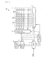
- Fig. 1 is a block diagram showing the schematic configuration of an electro-optical device according to an embodiment of the present invention.
- an electro-optical device 100 of this embodiment includes a display panel 1.
- the display panel 1 has plural m scanning lines 102, plural n data lines 104, the scanning lines 102 and the data lines 104 being orthogonal to each other (while electrically insulated), and pixel circuits 110 at intersections of the scanning lines 102 and the data lines 104.
- the electro-optical device 100 also includes a scanning line driving circuit 2 for driving the m scanning lines 102, a data line driving circuit 3 for driving the n data lines 104, a memory 4 for storing digital data Dpix for defining the brightness or gray level of each pixel of an image to be displayed, a control circuit 5 for controlling the components, an oscillator circuit 6 for generating a reference signal and a control signal for operating the components in synchronization, and a power supply circuit 7 for supplying power to the components.
- a scanning line driving circuit 2 for driving the m scanning lines 102
- a data line driving circuit 3 for driving the n data lines 104
- a memory 4 for storing digital data Dpix for defining the brightness or gray level of each pixel of an image to be displayed
- a control circuit 5 for controlling the components
- an oscillator circuit 6 for generating a reference signal and a control signal for operating the components in synchronization
- a power supply circuit 7 for supplying power to the components.
- the digital data Dpix stored in the memory 4 is supplied from an external apparatus, such as a computer, and defines the brightness of an organic EL element stored in each pixel circuit 110.
- the digital data Dpix has 6 bits and represents 64 gray levels (the sixth power of 2) ranging from "0" to "63" per pixel.
- the scanning line driving circuit 2 generates scanning signals Y1, Y2, Y3, ..., Ym for sequentially selecting the scanning lines 102 one at a time. Specifically, as shown in Fig. 3, the scanning line driving circuit 2 supplies a pulse with a width corresponding to one horizontal scanning period (1H) at the beginning of a vertical scanning period (1F) as the scanning signal Y1 to the first scanning line 102. From this point onward, the pulse is sequentially shifted and supplied as the scanning signals Y2, Y3, ..., Ym to the second, third, ..., m-th scanning lines 102. In general, when a scanning signal Yi supplied to an i-th (i is an integer satisfying 1 ⁇ i ⁇ m) scanning line 102 becomes the H level, it means that the scanning line 102 is selected.
- the scanning line driving circuit 2 In addition to the scanning signals Y1, Y2, Y3, ..., Ym, the scanning line driving circuit 2 generates luminous control signals Vg1, Vg2, Vg3, ..., Vgm by inverting the logical level of the scanning signals Y1, Y2, Y3, ..., Ym and supplies the luminous control signals Vg1, Vg2, Vg3, ..., Vgm to the display panel 1. This is not shown in Fig. 1.
- the data line driving circuit 3 has a current generating circuit, which is a feature of the present invention, for each data line 104.
- the data line driving circuit 3 supplies current indicating the gray level or brightness to the pixel circuits 110 located on the selected scanning line 102 via the data lines 104.
- the data line driving circuit 3 generates, for example, current in accordance with digital data read from the memory 4 and supplies the current to the pixel circuits 110 located on the selected scanning line 102 via the data lines 104.
- the details of the current generating circuit will be described hereinafter.
- the control circuit 5 controls selection of the scanning line 102 by the scanning line driving circuit 2. Also, the control circuit 5 reads digital data from the memory 4 in synchronization with the selection and supplies the digital data to the data line driving circuit 3. Therefore, currents in accordance with brightness levels of organic EL elements of the pixel circuits 110 located on the selected scanning line 102 are supplied to the pixel circuits 110 via the data lines 104.
- the components 1 to 7 of the electro-optical device 100 can be manufactured in various forms.
- the components 1 to 7 can be formed independently, or some or all of the components 1 to 7 can be integrated (for example, the scanning line driving circuit 2 and the data line driving circuit 3 can be integrated, or some or all of the components except for the display panel 1 can be formed by a programmable IC chip and the functions of these components can be realized by software using a program written to the IC chip).
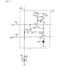
- Fig. 2 is a circuit diagram showing the configuration of one of the pixel circuits 110. All the pixel circuits 110 have the same configuration. In order to generalize and simplify the description of scanning signals, the pixel circuit 110 located at the intersection of the i-th scanning line 102 and one data line 104 will now be described.
- the pixel circuit 110 located at the intersection of the scanning line 102 and the data line 104 has four thin film transistors (hereinafter referred to as "TFT") 1102, 1104, 1106, and 1108, a capacitive element 1120, and an organic EL element 1130.
- TFT thin film transistors
- the source electrode of the p-channel TFT 1102 is connected to a power supply line 109 to which a high potential Vdd of the power supply is applied, and the drain electrode is connected to the drain electrode of the n-channel TFT 1104, the drain electrode of the n-channel TFT 1106, and the source electrode of the n-channel TFT 1108.
- a first end of the capacitive element 1120 is connected to the power supply line 109, and a second end is connected to the gate electrode of the TFT 1102 and the drain electrode of the TFT 1108.
- the gate electrode of the TFT 1104 is connected to the scanning line 102, and the source electrode is connected to the data line 104.
- the gate electrode of the TFT 1108 is connected to the scanning line 102.
- the gate electrode of the TFT 1106 is connected to a luminous control line 108, and the source electrode is connected to the anode of the organic EL element 1130.
- a luminous control signal Vgi is supplied by the scanning line driving circuit 2.
- an organic EL layer is held between the anode and the cathode, and light with brightness in accordance with forward current is emitted.
- the cathode of the organic EL element 1130 is a common electrode of all the pixel circuits 110 and is at a low (reference) potential of the power supply.
- the n-channel TFT 1108 conducts (on) the source electrode and the drain electrode.
- the n-channel TFT 1104 is also turned on, like the TFT 1108. Consequently, the current Iout generated by the current generating circuit 30 flows from the power supply line 109 ⁇ TFT 1102 ⁇ TFT 1104 ⁇ data line 104. At the same time, charge in accordance with the potential of the gate electrode of the TFT 1102 is accumulated in the capacitive element 1120.
- the TFTs 1104 and 1108 are turned off, while the charge accumulated in the capacitive element 1102 remains unchanged.
- the gate electrode of the TFT 1102 is maintained at the voltage when the current lout flowed.
- the n-channel TFT 1106 is turned on, and a current in accordance with the gate voltage flows between the source and the drain of the TFT 1102. Specifically, the current flows from the power supply line 109 ⁇ TFT 1102 ⁇ TFT 1106 ⁇ organic EL element 1130. Thus, the organic EL element 1130 emits light in accordance with the current value.
- the current value of the current flowing through the organic EL element 1130 is determined by the voltage of the gate electrode of the TFT 1102.
- the voltage of the gate electrode is the voltage maintained by the capacitive element 1102 when the current Iout flows through the data line 104 in response to the H-level scanning signal.
- the luminous control signal Vgi becomes the H level
- the current flowing through the organic EL element 1130 agrees with the current lout that flowed immediately before.
- the TFTs 1102 of all the pixel circuits 110 have different characteristics, it is possible to supply the same current to the organic EL elements 1130 included in the pixel circuits 110. It is thus possible to suppress display nonuniformity caused by the differences.
- the scanning signals Y1, Y2, Y3, ..., Ym exclusively become the H level one after another.
- the gate electrodes of the TFTs 1102 are maintained by the capacitive elements 1120 at the voltages when the current Iout in accordance with the brightness levels of the organic EL elements 1130 flowed.
- the transistors 1102, 1104, 1106, and 1108 do not need to be of the channel types described above.
- p or n channel can be can appropriately selected.
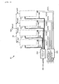
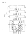
- Fig. 4 is a block diagram showing the configuration of one line of a current generating circuit 30 included in the data line driving circuit 3.
- a converter circuit 310 converts 6-bit digital data (D5 to D0) read from the memory 4 (see Fig. 1) into 19-bit digital data.
- the 19-bit digital data can be divided into four groups. Specifically, a first group has 5 bits S11 to S14 and S1F; a second group has 5 bits S21 to S24 and S2F; a third group has 5 bits S31 to S34 and S3F; and a fourth group has 4 bits S41 to S44.
- the first group is supplied to a circuit block C1; the second group is supplied to a circuit block C2; the third group is supplied to a circuit block C3; and the fourth group is supplied to a circuit block C4.
- the gray level range of a decimal value (D5 is the most significant bit) indicated by the 6-bit digital data (D0 to D5) has 64 steps from “0" to "63".
- the converter circuit 310 converts the 6-bit digital data into 19-bit digital data, such as that shown in Fig. 5, and outputs the 19-bit digital data. More specifically, as the gray level advances from “0" to "15”, the decimal value indicated by the bits S11 to S14 (S14 is the most significant bit) advances from "0" to "15” in a similar manner. All the other bits are converted so that they represent binary "0".
- the converter circuit 310 converts the 6-bit digital data into 19-bit digital data, such as that shown in Fig. 6, and outputs the 19-bit digital data. More specifically, as the gray level advances from “16" to "31", the decimal value indicated by the bits S21 to S24 (S24 is the most significant bit) advances from “0" to "15". The bits S11 to S14 and S1F are converted to be binary “1”, and all the other bits are converted to be binary "0".
- the converter circuit 310 converts the 6-bit digital data into 19-bit digital data, such as that shown in Fig. 7, and outputs the 19-bit digital data. More specifically, as the gray level advances from “32" to "47", the decimal value indicated by the bits S31 to S34 advances from “0" to "15". The bits S14 to S11 S1F, S24 to S21, and S2F are converted to be binary "1", and all the other bits are converted to be binary "0".
- the converter circuit 310 converts the 6-bit digital data into 19-bit digital data, such as that shown in Fig. 8, and outputs the 19-bit digital data. More specifically, as the gray level advances from “48” to "63", the decimal value indicated by the bits S41 to S44 (S44 is the most significant bit) advances from “0" to "15".
- the bits S11 to S14, S1F, S21 to S24, S2F, S31 to S34, and S3F are all converted to be binary "1".
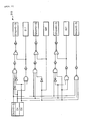
- Fig. 9 shows an example of the converter circuit 310 implemented by a logical circuit. Needless to say, the converter circuit 310 can be implemented not by a logical circuit but by a table having stored therein the details of conversion.
- a reference voltage generating circuit 320 generates reference voltages VCS1 to VCS4 and VCF1 to VCF4 from voltages V1 to V4 generated by the power supply circuit 7.
- the reference voltage generating circuit 320 generates, for example, the reference voltages VCS1 and VCF1 from the voltage V1 by a current mirror circuit, such as that shown in Fig. 10.
- a current mirror circuit such as that shown in Fig. 10.
- the voltage V1 output from the power supply circuit 7 shown in Fig. 1 is supplied to the input side of the current mirror circuit, while the reference voltages VCS1 and VCF1 are removed from the output side.
- Similar current mirror circuits generate the reference voltages VCS2 and VCF2 from the voltage V2, the reference voltages VCS3 and VCF3 from the voltage V3, and the reference voltage VCF4 from the voltage V4, respectively.
- the circuit block C1 is allocated to "0" to "15" of the decimal-value gray levels "0" to "63” indicated by the 6-bit digital data (D0 to D5). More specifically, as shown in Fig. 11, switches 11a to 11d and 11e are turned on/off in accordance with the bits S11 to S14 and S1F of the 19-bit data generated by conversion by the converter circuit 310, and elemental currents i11 to i14 and i1F output by FETs (Field-Effect Transistor) 10a to 10e and 10f to 10j are combined to generate a sub-current Iout1.
- FETs Field-Effect Transistor
- the FET configuration is such that the FETs are grouped into two stages, namely, the FETs 10a to 10e and the FETs 10f to 10j, in order to have stable characteristics of the output current Iout.
- the circuit block C2 is allocated to "16" to "31" of the decimal-value gray levels "0" to "63” indicated by the digital data (D0 to D5).
- the circuit block C2 is equivalent to the circuit block C1.
- the circuit block C2 appropriately selects elemental currents i21 to i24 and i2F in accordance with the bits S21 to S24 and S2F of the 19-bit data, which is generated by conversion by the converter circuit 310, and combines the selected elemental currents to generate a sub-current Iout2.
- the circuit block C3 is allocated to "32" to "47” of the decimal-value gray levels "0" to "63” indicated by the digital data (D0 to D5).
- the circuit block C3 is equivalent to the circuit blocks C1 and C2.
- the circuit block C3 appropriately selects elemental currents i31 to i34 and i3F in accordance with the bits S31 to S34 and S3F of the 19-bit data, which is generated by conversion by the converter circuit 31, and combines the selected elemental currents to generate a sub-current Iout3.
- the circuit block C4 is allocated to "48" to "63” of the decimal-value gray levels "0" to "63” indicated by the digital data (D0 to D5).
- the circuit block C4 is equivalent to the circuit block C1 except for the fact that the circuit block C4 does not have parts corresponding to the switch 11f and the FETs 10e and 10j (enclosed by a dotted line 50).
- the circuit block C4 appropriately selects elemental currents i41 to i44 in accordance with the bits S41 to S44 and combines the selected elemental currents to generate a sub-current Iout4.
- the circuit enclosed by the dotted line 50 in the circuit block C1 is for selecting the elemental current i1F.
- the elemental current i1F is used to add the elemental currents i11 to i14 when generating the sub-current Iout1 corresponding to the decimal-value gray level "16" (the minimum value of a range allocated to the circuit block adjacent to the top side of the circuit block C1) indicated by the digital data (D5 to D0).
- the circuits enclosed by the dotted lines 50 in the circuit blocks C2 and C3 are for selecting the elemental currents i2F and i3F.
- the elemental current i2F is used to add the elemental currents i21 to i24 when generating the sub-current Iout2 corresponding to the gray level "32".
- the elemental current i3F is used to add the elemental currents i31 to i34 when generating the sub-current Iout3 corresponding to the gray level "48".
- the sub-current Iout4 greater than or equal to the sum of the elemental currents i21 to i24 is unnecessary.
- the current block C4 does not have a circuit corresponding to the dotted line 50.
- the sub-currents Iout1 to Iout4 generated by the circuit blocks C1 to C4 are combined by a combining current line 32 to generate a main current Iout, and the main current Iout is output to the corresponding data line 104.
- the bits S11 to S14 are converted so that a decimal value represented by these 4 bits (S14 is the most significant bit) sequentially advances from “0" to "15”.
- the switches 11a to 11d in the circuit block C1 are turned on/off, and the elemental currents i11 to i14 are appropriately selected.
- the sub-current Iout1 is generated.
- the main current Iout when the gray level is within the range from “0" to “15” can be represented only by the sub-current Iout1 which is generated by combining, by the circuit block C1, the appropriately selected elemental currents i11 to i14.
- the bits S11 to S14 and S1F are converted to be binary "1".
- all the switches 11a to 11d and 11e in the circuit block C1 are turned on.
- the sub-current Iout1 becomes the maximum value indicated by the sum of the elemental currents i11 to i14 and i1F.
- the bits S21 to S24 are converted so that a decimal value represented by the four bits (S24 is the most significant bit) sequentially advances from “0" to "15".
- the elemental currents i21 to i24 are appropriately selected by the circuit block C2, and hence the sub-current Iout2 is generated.
- the main current lout when the gray level is within the range from “16" to "31” is obtained by adding the sub-current Iout2, which is generated by combining the appropriately selected elemental currents i21 to i24 by the circuit block C2, to the sub-current Iout1 having the maximum value.
- the gray level is "16" (the minimum value of the range allocated to the circuit block C2), more specifically, the current value Iout2 is zero.
- the main current Iout can be indicated by the current value Iout1 having the maximum value.
- the sub-current Iout1 by the circuit block C1 is the sum of the elemental currents i11 to i14 and i1F.
- the sub-current Iout2 by the circuit block C2 is the sum of the elemental currents i21 to i24 and i2F.
- the bits S31 to S34 are converted so that the decimal value indicated by the four bits (S34 is the most significant bit) sequentially advances from “0" to "15".
- the elemental currents i31 to i34 are appropriately selected by the circuit block C3, and hence the sub-current Iout3 is generated.
- the main current lout when the gray scale is within the range from "32" to "47” is generated by adding the sub-current Iout3, which is generated by adding the appropriately selected elemental currents i31 to i34 by the circuit block C3, to the sum of the sub-currents Iout1 and Iout2, both having maximum values.
- the gray level is "32" (minimum value of the range allocated to the circuit block C3), more specifically, the sub-current Iout3 is zero.
- the main current Iout can be indicated by the sum of the sub-currents Iout1 and Iout2, both having maximum values.
- the sub-current Iout1 by the circuit block 1 is the sum of the elemental currents i11 to i14 and i1F.
- the sub-current Iout2 by the circuit block C2 is the sum of the elemental currents i21 to i24 and i2F.
- the sub-current Iout3 by the circuit block C3 is the sum of the elemental currents i31 to i34 and i3F.
- the bits S41 to S44 are converted so that the decimal value indicated by the four bits (S44 is the most significant bit) sequentially advances from “0" to "15”.
- the elemental currents i41 to i44 are appropriately selected, and the sub-current Iout4 is generated.
- the main current Iout when the gray level is within the range from "48" to "63” is generated by adding the sub-current Iout4, which is generated by adding the appropriately selected elemental currents i41 to 44 by the circuit block C4, to the sum of the sub-currents Iout1 Iout2, and Iout3, all having maximum values.
- the gray level is "48” (minimum value of the range allocated to the circuit block C4), more specifically, the sub-current Iout4 is zero.
- the main current Iout is indicated by the sum of the sub-currents Iout1 Iout2, and Iout3, all having maximum values.
- the reference voltages VCS1 to VCS4 (VCF1 to VCF4) generated by the reference voltage generating circuit 320 have the relationship VCS1 ⁇ VCS2 ⁇ VCS3 ⁇ VCS4 (VCF1 ⁇ VCF2 ⁇ VCF3 ⁇ VCF4).
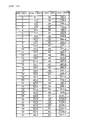
- the main currents Iout corresponding to the gray levels "0" to "63" indicated by the digital data (D0 to D5) have values shown in Fig. 13.
- the gray level/main current characteristics are, as shown in Fig. 14, indicated by a simulated ⁇ curve generated by four straight lines.
- the main current Iout when the gray level is within the range from “0" to “16” is the sub-current Iout1 generated by combining the appropriately selected elemental currents i11 to i14 and i1F by the circuit block C1.
- the main current Iout has an approximately linear characteristic within this range.
- the slope is determined by the reference voltage VCS1 (VSF1). Since the weights of the elemental currents i11 and i1F are "1", the main current Iout when the gray level is "16" is on an extension of the characteristic of the gray levels from "0" to "15".
- the main current lout when the gray level is within the range from “16” to “32” is the sum of the sub-current Iout1 having the maximum value in the circuit block C1 and the sub-current Iout2 generated by combining the appropriately selected elemental currents i21 to i24 and i2F by the circuit block C2.
- the main current lout has an approximately linear characteristic in this range, which is continuous with the approximately linear characteristic when the gray level is within the range from "0" to "16”.
- the slope of the main current Iout when the gray level is within the range from “16” to “32” is determined by the reference voltage VCS2 (VSF2). Since the weights of the elemental currents i21 and i2F are "1", the main current lout when the gray level is "32” is on an extension of the characteristic of the gray levels from "16” to "31".
- the main current Iout when the gray level is within the range from "32" to “48” is the sum of the sub-currents Iout1 and Iout2 having maximum values and the sub-current Iout3 generated by combining the appropriately selected elemental currents i31 to i34 and i3F by the circuit block C3.
- the main current Iout has an approximately linear characteristic in this range, which is continuous with the approximately linear characteristic when the gray level is within the range from "16" to "32".
- the slope of the main current lout when the gray level is within the range from "32" to "48” is determined by the reference voltage VCS3 (VSF3).
- the main current lout when the gray level is within the range from "48" to “63” is the sum of the sub-currents Iout1 Iout2, and Iout3 having maximum values and the sub-current Iout4 generated by combining the appropriately selected elemental currents i41 to i44 by the circuit block C4.
- the main current Iout has an approximately linear characteristic in this range, which is continuous with the approximately linear characteristic when the gray level is within the range from "32" to "48".
- the slope of the main current Iout when the gray level is within the range from "48” to "63” is determined by the reference voltage VCS4 (VSF4).
- the characteristic of the main current Iout relative to the gray level can be variously set.
- the main current Iout increases, as shown in Fig. 15, approximately linearly over the whole range of gray levels "0" to "63".
- VCS1 VCS2 > VCS3 > VCS4
- VCS1 VCS2
- VCS3 VCS4
- VCS1 VCS2
- VCS3 VCS3
- the voltages V1 to V4 generated by the power supply circuit 7 are set individually.
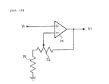
- the configuration for individually setting the voltage V1 an example shown in Fig. 18 can be used.
- the output of an operational amplifier 71 is supplied as a negative feedback input using a variable resistor 73 and a resistor 75.
- the resistance of the variable resistor 73 can be adjusted manually or can be adjusted by an analog switch.
- the characteristics of the main currents relative to the gray levels are represented by four continuous approximately linear lines. It is thus possible to simulate ⁇ characteristics of the display panel 1 in various manners in accordance with the purpose and use.
- the current generating circuit 30 64 types of main currents lout can be generated by four types of reference voltages using V1 to V4 and a logic power supply voltage. Thus, the number of necessary voltage sources can be very small. Thus, the configuration becomes simple, the power consumption can be reduced, and the durability can be enhanced.
- the current generating circuit 30 generates the main currents Iout corresponding to 64 gray levels by combining the four sub-currents Iout1 to Iout4 generated by the circuit blocks C1 to C4.
- the number of circuit blocks can be increased (by decreasing the number of FETs 10f to 10j belonging to one circuit block), and smoother non-linear characteristics can be achieved.
- the number of circuit blocks can be reduced (by increasing the number of FETs 10f to 10j belonging to one circuit block), and the conversion burden on the converter circuit 310 can be reduced (the number of data lines defining on/off of switches of the circuit block can be reduced).
- FETs are used to generate elemental currents in the circuit blocks
- bipolar transistors can be used alternatively.
- the main current Iout is zero, which is the minimum value, when the gray level is "0" (see Fig. 13).
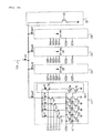
- the value of the lower limit for the main current lout can be defined by the voltage V0.
- the current flowing through the offset current circuit 51 is offset against the sum of the sub-currents Iout1 to Iout4 combined to form the main current Iout. Therefore, the minimum value of the main current lout can be set to the value of the lower limit instead of zero.
- the currents to be supplied to the organic EL elements 1130 of the pixel circuits 110 located on the scanning line 102 is supplied via the data lines 104.
- a pre-charge circuit 53 can be provided for each data line 104.
- the pre-charge circuit 53 includes an FET 532 for causing a pre-charge current Ip in accordance with a gate voltage Vpre to flow and a switch 534 for pre-charging the data line 104 by being turned on in response to a signal Dp before the main current Iout flows through the data line 104 and causing the pre-charge current Ip to flow through the data line 104.
- the period required for the current flowing through the data line 104 to reach the target main current Iout can be reduced, compared with a case in which the pre-charge circuit 53 is not used. Accordingly, driving can be performed at a higher speed.
- the luminous control signals Vg1, Vg2, Vg3, ..., Vgm are generated by inverting, by the scanning line driving circuit 2, the logical level of the scanning signals Y1, Y2, Y3, ..., Ym and are supplied.
- the luminous control signals Vg1, Vg2, Vg3, ..., Vgm can be supplied by a separate circuit.
- the luminous control signals Vg1, Vg2, Vg3, ..., Vgm can be generated by reducing the periods during which the luminous control signals Vg1, Vg2, Vg3, ..., Vgm are at the active level (H level).
- the current generating circuit 30 which is the feature of the present invention, is applied to the data line driving circuit of the organic EL panel.
- the current generating circuit can be applied to various display panels other than the organic EL panel, such as an FED (Field Emission Display).
- Fig. 21 is a perspective view showing the configuration of a mobile personal computer to which the electro-optical device 100 is applied.
- a personal computer 2100 includes a main unit 2104 with a keyboard 2102 and the electro-optical device 100 as a display unit.
- Fig. 22 is a perspective view showing the configuration of a cellular phone to which the foregoing electro-optical device is applied.
- a cellular phone 2200 includes a plurality of operation buttons 2202, an earpiece 2204, a mouthpiece 2206, and the electro-optical device 100.
- Fig. 23 is a perspective view showing the configuration of a digital still camera having a finder to which the electro-optical device 100 is applied.
- a digital still camera 2300 uses an image pickup device such as a CCD (Charge Coupled Device) to perform photoelectric conversion of an optical image of a subject and generates/stores an image pickup signal.
- the above-described electro-optical device 100 is provided on the back of a main portion 2302 of the digital still camera 2300. Since the electro-optical device 100 displays an image in accordance with the image pickup signal, the electro-optical device 100 functions as a finder for displaying the subject.
- a light receiving unit 2304 including an optical lens and the CCD is provided on the front side of the main portion 2302 (the back side in Fig. 23).
- a video signal output terminal 2312 for performing external display and an input/output terminal 2314 for data communication are provided on the lateral side of a case 2302.
- Electronic apparatuses to which the electro-optical device 100 is applicable include the personal computer shown in Fig. 21, the cellular phone shown in Fig. 22, the digital still camera shown in Fig. 23, a liquid crystal television, a viewfinder-type or a monitor-direct-viewing-type video cassette recorder, a car navigation system, a pager, an electronic notebook, an electronic calculator, a word processor, a workstation, a video phone, a POS terminal, and a device with a touch panel.
- the electro-optical device 100 is applicable to display units of these various electronic apparatuses.
- the circuit configuration can be simplified, and the power consumption can be suppressed.
Landscapes
- Engineering & Computer Science (AREA)
- Physics & Mathematics (AREA)
- Computer Hardware Design (AREA)
- General Physics & Mathematics (AREA)
- Theoretical Computer Science (AREA)
- Control Of Indicators Other Than Cathode Ray Tubes (AREA)
- Control Of El Displays (AREA)
- Electroluminescent Light Sources (AREA)
- Liquid Crystal Display Device Control (AREA)
Abstract
Description
- The present invention relates to current generating circuits for use in driving display panels, such as organic EL (Electronic Luminescence) panels, and more specifically, it relates to a current generating circuit for generating current with non-linear characteristics with respect to digital data indicating the brightness of a display panel.
- Generally, in liquid crystal panels, a change in gray level (brightness) of a pixel is not proportional to the voltage applied to the pixel. When driving liquid crystal panels, voltages with non-linear characteristics with respect to the linear gray scale of pixels (generally defined by digital data) are output. Thus, it looks as if the gray scale changes linearly.
- On the other hand, the human visual characteristics are generally known as having logarithmic or exponential characteristics. If the brightness, represented as the gray level, changes linearly, it may not appear to the human eye that the gray level changes linearly. In view of these circumstances, an electro-optical device should have logarithmic or exponential gray scale characteristics, and hence it appears to the human eye that the gray scale has linear characteristics. A series of these processes may be referred to as γ correction.
- Recently, organic EL panels have been attracting interest as next-generation display panels. This is because, unlike liquid crystal elements for simply changing the light transmission, organic EL elements used as electro-optical elements in organic EL panels are self-luminous elements which emit light by themselves. For this reason, organic EL panels have excellent characteristics, such as a wider viewing angle, a higher contrast, and a higher response speed than, liquid crystal panels.
- Unlike voltage-driven liquid crystal elements, organic EL elements are so-called current-driven elements. When driving organic EL elements, it is necessary to generate current, not voltage, in accordance with the gray level of a pixel. As an example of a known current generating circuit for generating current, the configuration such as that shown in Fig. 24 can be used.
- In this drawing, a voltage generating circuit is a current-adding-type D/A converter, which switches on/off
transistors 20a to 20f in accordance with 6-bit digital data (D0 to D5) indicating the gray level of a pixel to select elemental currents i1 to i6 and which combines the selected elemental currents to obtain a current Iout in accordance with the gray level. - In organic EL elements, as in liquid crystals, it is necessary to perform γ correction in order to generate logarithmic or exponential gray scale characteristics. In the current generating circuit shown in Fig. 24, the output current generated relative to 6-bit digital data indicating the gray level of a pixel has linear characteristics. If the current generating circuit remains unchanged, it is impossible to perform sufficient γ correction.
- In order to generate a current with non-linear characteristics using such a current generating circuit, for example, it is necessary to have a scheme to prepare in advance a plurality of voltage sources and to individually control gate currents of the
transistors 20a to 20f. In this scheme, as the number of gray levels increases, so does the number of necessary voltage sources. Thus, the circuit configuration becomes complex. - In general, as the number of voltage sources increases, the power consumed by generating voltage increases. This scheme is thus unsuitable for use in organic EL panels of electronic apparatuses such as mobile personal computers and cellular phones, for which there are strong demands to reduce the power consumption.
- In view of the foregoing circumstances, it is an object of the present invention to provide a current generating circuit with a simple circuit configuration and low power consumption.
- In order to achieve the foregoing objects, according to an aspect of the present invention, a current generating circuit is provided including a plurality of circuit blocks for outputting sub-currents by selecting elemental currents from among a plurality of elemental currents in accordance with input digital data; and a combining circuit for outputting a main current by combining the sub-currents.
- Preferably, each of the circuit blocks generates the plurality of elemental currents by transistors having different gain coefficients.
- Preferably, the transistors include a combination of transistors in which the ratios of the gain coefficients are the binary weights.
- Preferably, the transistors are field effect transistors, and a common reference voltage is supplied to gate electrodes of the transistors of each of the circuit blocks.
- Similarly, in order to achieve the foregoing objects, according to another aspect of the present invention, a current generating circuit is provided including a plurality of circuit blocks for generating sub-currents; and a combining circuit for outputting a main current by combining the sub-currents generated by the circuit blocks. Each of the circuit blocks is allocated to a corresponding range obtained by dividing a possible range of input digital data. When the digital data value is below the range allocated to each of the circuit blocks, the circuit block generates an approximately zero sub-current. When the digital data value is within the range allocated to each of the circuit blocks, the circuit block generates a sub-current having an approximately linear characteristic in accordance with the digital data. When the digital data value is above the range allocated to each of the circuit blocks, the circuit block generates a sub-current corresponding to the minimum value of the range of digital data allocated to an upper block adjacent to the circuit block.
- Preferably, the approximately linear characteristic of the circuit block can be set individually for each of the circuit blocks.
- Preferably, the current generating circuit further includes an offset current path for defining the value of a lower limit for the main current.
- An electro-optical device includes a plurality of scanning lines; a plurality of data lines; a scanning line driving circuit for driving the scanning lines; a data line driving circuit for driving the data lines; and electro-optical elements located at intersections of the scanning lines and the data lines. The data line driving circuit includes the above-described current generating circuit and supplies a main current generated by the current generating circuit to each of the data lines.
- In the electro-optical device, preferably, the electro-optical elements are driven elements driven by current.
- The driven elements may be organic electro-luminescence elements.
- Preferably, the electro-optical device further includes a memory for storing data for defining brightness gray levels of the organic electro-luminescence elements; and a control circuit for reading the data from the memory and supplying the data as the digital data to the data line driving circuit.
- Preferably, the electro-optical device further includes an oscillator circuit for supplying a reference operation signal functioning as an operation reference.
- According to another aspect of the present invention, an electronic apparatus has the above-described electro-optical device mounted thereon.
- Embodiments of the present invention will now be described by way of further example only and with reference to the accompanying drawings, in which:-
- Fig. 1 is a block diagram showing the configuration of an electro-optical device according to an embodiment of the present invention.
- Fig. 2 is a diagram showing the configuration of a pixel circuit in the electro-optical device.
- Fig. 3 is a timing chart for describing the operation of the pixel circuit.
- Fig. 4 is a block diagram showing the configuration of a current generating circuit included in a data line driving circuit of the electro-optical device.
- Fig. 5 is an illustration showing the contents of conversion performed by a converter circuit of the current generating circuit.
- Fig. 6 is an illustration showing the contents of conversion performed by the converter circuit of the current generating circuit.
- Fig. 7 is an illustration showing the contents of conversion performed by the converter circuit of the current generating circuit.
- Fig. 8 is an illustration showing the contents of conversion performed by the converter circuit of the current generating circuit.
- Fig. 9 is a diagram showing an example of the converter circuit.
- Fig. 10 is a diagram showing a reference voltage generating circuit of the current generating circuit.
- Fig. 11 is a diagram showing the configuration of a current selecting circuit of the current generating circuit.
- Fig. 12 is an illustration of examples of elemental currents generated by the current generating circuit.
- Fig. 13 is an illustration of examples of main currents generated by the current generating circuit.
- Fig. 14 is an illustration of a gray level/main current characteristic of the current generating circuit.
- Fig. 15 is an illustration of the gray level/main current characteristic of the current generating circuit.
- Fig. 16 is an illustration of the gray level/main current characteristic of the current generating circuit.
- Fig. 17 is an illustration of the gray level/main current characteristic of the current generating circuit.
- Fig. 18 is a diagram showing an example of a portion of a power supply circuit for generating a voltage V1.
- Fig. 19 is a diagram showing an application of the current generating circuit.
- Fig. 20 is a diagram showing an application of the current generating circuit.
- Fig. 21 is a perspective view showing the configuration of a mobile personal computer to which the electro-optical device is applied.
- Fig. 22 is a perspective view showing the configuration of a cellular phone to which the electro-optical device is applied.
- Fig. 23 is a perspective view showing the configuration of a digital still camera to which the electro-optical device is applied.
- Fig. 24 is a diagram showing the configuration of a known current generating circuit.
-
- With reference to the drawings, embodiments of the present invention will now be described.
- Fig. 1 is a block diagram showing the schematic configuration of an electro-optical device according to an embodiment of the present invention.
- As shown in this drawing, an electro-
optical device 100 of this embodiment includes adisplay panel 1. Thedisplay panel 1 has pluralm scanning lines 102, pluraln data lines 104, thescanning lines 102 and thedata lines 104 being orthogonal to each other (while electrically insulated), andpixel circuits 110 at intersections of thescanning lines 102 and the data lines 104. The electro-optical device 100 also includes a scanningline driving circuit 2 for driving them scanning lines 102, a dataline driving circuit 3 for driving then data lines 104, amemory 4 for storing digital data Dpix for defining the brightness or gray level of each pixel of an image to be displayed, acontrol circuit 5 for controlling the components, anoscillator circuit 6 for generating a reference signal and a control signal for operating the components in synchronization, and apower supply circuit 7 for supplying power to the components. - Of these components, the digital data Dpix stored in the
memory 4 is supplied from an external apparatus, such as a computer, and defines the brightness of an organic EL element stored in eachpixel circuit 110. In this embodiment, in order to simplify the description, the digital data Dpix has 6 bits and represents 64 gray levels (the sixth power of 2) ranging from "0" to "63" per pixel. - In contrast, the scanning
line driving circuit 2 generates scanning signals Y1, Y2, Y3, ..., Ym for sequentially selecting thescanning lines 102 one at a time. Specifically, as shown in Fig. 3, the scanningline driving circuit 2 supplies a pulse with a width corresponding to one horizontal scanning period (1H) at the beginning of a vertical scanning period (1F) as the scanning signal Y1 to thefirst scanning line 102. From this point onward, the pulse is sequentially shifted and supplied as the scanning signals Y2, Y3, ..., Ym to the second, third, ..., m-th scanning lines 102. In general, when a scanning signal Yi supplied to an i-th (i is an integer satisfying 1 ≤ i ≤m) scanningline 102 becomes the H level, it means that thescanning line 102 is selected. - In addition to the scanning signals Y1, Y2, Y3, ..., Ym, the scanning
line driving circuit 2 generates luminous control signals Vg1, Vg2, Vg3, ..., Vgm by inverting the logical level of the scanning signals Y1, Y2, Y3, ..., Ym and supplies the luminous control signals Vg1, Vg2, Vg3, ..., Vgm to thedisplay panel 1. This is not shown in Fig. 1. - The data line driving
circuit 3 has a current generating circuit, which is a feature of the present invention, for eachdata line 104. The data line drivingcircuit 3 supplies current indicating the gray level or brightness to thepixel circuits 110 located on the selectedscanning line 102 via the data lines 104. Specifically, the dataline driving circuit 3 generates, for example, current in accordance with digital data read from thememory 4 and supplies the current to thepixel circuits 110 located on the selectedscanning line 102 via the data lines 104. The details of the current generating circuit will be described hereinafter. - The
control circuit 5 controls selection of thescanning line 102 by the scanningline driving circuit 2. Also, thecontrol circuit 5 reads digital data from thememory 4 in synchronization with the selection and supplies the digital data to the data line drivingcircuit 3. Therefore, currents in accordance with brightness levels of organic EL elements of thepixel circuits 110 located on the selectedscanning line 102 are supplied to thepixel circuits 110 via the data lines 104. - The
components 1 to 7 of the electro-optical device 100 can be manufactured in various forms. For example, thecomponents 1 to 7 can be formed independently, or some or all of thecomponents 1 to 7 can be integrated (for example, the scanningline driving circuit 2 and the data line drivingcircuit 3 can be integrated, or some or all of the components except for thedisplay panel 1 can be formed by a programmable IC chip and the functions of these components can be realized by software using a program written to the IC chip). - The
pixel circuits 110 of the electro-optical device 100 will now be described. Fig. 2 is a circuit diagram showing the configuration of one of thepixel circuits 110. All thepixel circuits 110 have the same configuration. In order to generalize and simplify the description of scanning signals, thepixel circuit 110 located at the intersection of the i-th scanning line 102 and onedata line 104 will now be described. - As shown in this drawing, the
pixel circuit 110 located at the intersection of thescanning line 102 and thedata line 104 has four thin film transistors (hereinafter referred to as "TFT") 1102, 1104, 1106, and 1108, acapacitive element 1120, and anorganic EL element 1130. - Of these components, the source electrode of the p-
channel TFT 1102 is connected to a power supply line 109 to which a high potential Vdd of the power supply is applied, and the drain electrode is connected to the drain electrode of the n-channel TFT 1104, the drain electrode of the n-channel TFT 1106, and the source electrode of the n-channel TFT 1108. - A first end of the
capacitive element 1120 is connected to the power supply line 109, and a second end is connected to the gate electrode of theTFT 1102 and the drain electrode of theTFT 1108. The gate electrode of theTFT 1104 is connected to thescanning line 102, and the source electrode is connected to thedata line 104. The gate electrode of theTFT 1108 is connected to thescanning line 102. - In contrast, the gate electrode of the
TFT 1106 is connected to aluminous control line 108, and the source electrode is connected to the anode of theorganic EL element 1130. Concerning theluminous control line 108, a luminous control signal Vgi is supplied by the scanningline driving circuit 2. Concerning theorganic EL element 1130, an organic EL layer is held between the anode and the cathode, and light with brightness in accordance with forward current is emitted. The cathode of theorganic EL element 1130 is a common electrode of all thepixel circuits 110 and is at a low (reference) potential of the power supply. - In this arrangement, when a scanning signal Yi supplied to the
scanning line 102 becomes the H level, the n-channel TFT 1108 conducts (on) the source electrode and the drain electrode. TheTFT 1102, in which the gate electrode and the drain electrode are connected to each other, functions as a diode. When the scanning signal Yi supplied to thescanning line 102 becomes the H level, the n-channel TFT 1104 is also turned on, like theTFT 1108. Consequently, the current Iout generated by thecurrent generating circuit 30 flows from the power supply line 109 →TFT 1102 →TFT 1104 →data line 104. At the same time, charge in accordance with the potential of the gate electrode of theTFT 1102 is accumulated in thecapacitive element 1120. - When the scanning signal Yi becomes the L level, the
TFTs capacitive element 1102 remains unchanged. Thus, the gate electrode of theTFT 1102 is maintained at the voltage when the current lout flowed. - When the scanning signal Yi becomes the L level, the luminous control signal Vgi becomes the H level. Thus, the n-
channel TFT 1106 is turned on, and a current in accordance with the gate voltage flows between the source and the drain of theTFT 1102. Specifically, the current flows from the power supply line 109 →TFT 1102 →TFT 1106 →organic EL element 1130. Thus, theorganic EL element 1130 emits light in accordance with the current value. - The current value of the current flowing through the
organic EL element 1130 is determined by the voltage of the gate electrode of theTFT 1102. The voltage of the gate electrode is the voltage maintained by thecapacitive element 1102 when the current Iout flows through thedata line 104 in response to the H-level scanning signal. Thus, when the luminous control signal Vgi becomes the H level, the current flowing through theorganic EL element 1130 agrees with the current lout that flowed immediately before. - If the
TFTs 1102 of all thepixel circuits 110 have different characteristics, it is possible to supply the same current to theorganic EL elements 1130 included in thepixel circuits 110. It is thus possible to suppress display nonuniformity caused by the differences. - Although one
pixel circuit 110 has been described, since mpixel circuits 110 share the i-th scanning line 102, them pixel circuits 110 operate in a similar manner when the scanning signal Yi becomes the H level. - As shown in Fig. 3, the scanning signals Y1, Y2, Y3, ..., Ym exclusively become the H level one after another. In all the
pixel circuits 110, the gate electrodes of theTFTs 1102 are maintained by thecapacitive elements 1120 at the voltages when the current Iout in accordance with the brightness levels of theorganic EL elements 1130 flowed. - The
transistors transistors - The current generating circuit, which is the feature of the present invention, will now be described. Fig. 4 is a block diagram showing the configuration of one line of a
current generating circuit 30 included in the dataline driving circuit 3. - In this drawing, a
converter circuit 310 converts 6-bit digital data (D5 to D0) read from the memory 4 (see Fig. 1) into 19-bit digital data. The 19-bit digital data can be divided into four groups. Specifically, a first group has 5 bits S11 to S14 and S1F; a second group has 5 bits S21 to S24 and S2F; a third group has 5 bits S31 to S34 and S3F; and a fourth group has 4 bits S41 to S44. The first group is supplied to a circuit block C1; the second group is supplied to a circuit block C2; the third group is supplied to a circuit block C3; and the fourth group is supplied to a circuit block C4. - The details of conversion by the
converter circuit 310 will now be described. The gray level range of a decimal value (D5 is the most significant bit) indicated by the 6-bit digital data (D0 to D5) has 64 steps from "0" to "63". When the gray level of the decimal value is "0" to "15", theconverter circuit 310 converts the 6-bit digital data into 19-bit digital data, such as that shown in Fig. 5, and outputs the 19-bit digital data. More specifically, as the gray level advances from "0" to "15", the decimal value indicated by the bits S11 to S14 (S14 is the most significant bit) advances from "0" to "15" in a similar manner. All the other bits are converted so that they represent binary "0". - When the gray level of the decimal value is "16" to "31", the
converter circuit 310 converts the 6-bit digital data into 19-bit digital data, such as that shown in Fig. 6, and outputs the 19-bit digital data. More specifically, as the gray level advances from "16" to "31", the decimal value indicated by the bits S21 to S24 (S24 is the most significant bit) advances from "0" to "15". The bits S11 to S14 and S1F are converted to be binary "1", and all the other bits are converted to be binary "0". - When the gray level of the decimal value is "32" to "47", the
converter circuit 310 converts the 6-bit digital data into 19-bit digital data, such as that shown in Fig. 7, and outputs the 19-bit digital data. More specifically, as the gray level advances from "32" to "47", the decimal value indicated by the bits S31 to S34 advances from "0" to "15". The bits S14 to S11 S1F, S24 to S21, and S2F are converted to be binary "1", and all the other bits are converted to be binary "0". - When the gray level of the decimal value is "48" to "63", the
converter circuit 310 converts the 6-bit digital data into 19-bit digital data, such as that shown in Fig. 8, and outputs the 19-bit digital data. More specifically, as the gray level advances from "48" to "63", the decimal value indicated by the bits S41 to S44 (S44 is the most significant bit) advances from "0" to "15". The bits S11 to S14, S1F, S21 to S24, S2F, S31 to S34, and S3F are all converted to be binary "1". - Fig. 9 shows an example of the
converter circuit 310 implemented by a logical circuit. Needless to say, theconverter circuit 310 can be implemented not by a logical circuit but by a table having stored therein the details of conversion. - Referring again to Fig. 4, a reference
voltage generating circuit 320 generates reference voltages VCS1 to VCS4 and VCF1 to VCF4 from voltages V1 to V4 generated by thepower supply circuit 7. - The reference
voltage generating circuit 320 generates, for example, the reference voltages VCS1 and VCF1 from the voltage V1 by a current mirror circuit, such as that shown in Fig. 10. In this drawing, the voltage V1 output from thepower supply circuit 7 shown in Fig. 1 is supplied to the input side of the current mirror circuit, while the reference voltages VCS1 and VCF1 are removed from the output side. Similar current mirror circuits generate the reference voltages VCS2 and VCF2 from the voltage V2, the reference voltages VCS3 and VCF3 from the voltage V3, and the reference voltage VCF4 from the voltage V4, respectively. - The circuit block C1 is allocated to "0" to "15" of the decimal-value gray levels "0" to "63" indicated by the 6-bit digital data (D0 to D5). More specifically, as shown in Fig. 11,
switches 11a to 11d and 11e are turned on/off in accordance with the bits S11 to S14 and S1F of the 19-bit data generated by conversion by theconverter circuit 310, and elemental currents i11 to i14 and i1F output by FETs (Field-Effect Transistor) 10a to 10e and 10f to 10j are combined to generate a sub-current Iout1. - When a predetermined voltage is supplied to the gate electrode and the source electrode of an FET, the current flowing through the FET defines a gain coefficient β. The FETs 10f to 10j are set to have ratios of gain coefficients β of 10f:10g:10h:10i:10j = 1 : 2 : 4 : 8 1.
- The reference voltage VCS1 is commonly supplied to the gate electrodes of the FETs 10a to 10e, and the reference voltage VCF1 is commonly supplied to the gate electrodes of the FETs 10f to 10j. Accordingly, the ratios of elemental currents i1 to i4 and i1F are i1:i2:i3:i4:i1F = 1 : 2 : 4 : 8 : 1.
- In the circuit block C1, the FET configuration is such that the FETs are grouped into two stages, namely, the FETs 10a to 10e and the FETs 10f to 10j, in order to have stable characteristics of the output current Iout.
- Theoretically, it is possible to form a circuit having an equivalent function by only using the
FETs 10f to 10j. - The circuit block C2 is allocated to "16" to "31" of the decimal-value gray levels "0" to "63" indicated by the digital data (D0 to D5). The circuit block C2 is equivalent to the circuit block C1. In other words, the circuit block C2 appropriately selects elemental currents i21 to i24 and i2F in accordance with the bits S21 to S24 and S2F of the 19-bit data, which is generated by conversion by the
converter circuit 310, and combines the selected elemental currents to generate a sub-current Iout2. - The circuit block C3 is allocated to "32" to "47" of the decimal-value gray levels "0" to "63" indicated by the digital data (D0 to D5). The circuit block C3 is equivalent to the circuit blocks C1 and C2. In other words, the circuit block C3 appropriately selects elemental currents i31 to i34 and i3F in accordance with the bits S31 to S34 and S3F of the 19-bit data, which is generated by conversion by the
converter circuit 31, and combines the selected elemental currents to generate a sub-current Iout3. - The circuit block C4 is allocated to "48" to "63" of the decimal-value gray levels "0" to "63" indicated by the digital data (D0 to D5). The circuit block C4 is equivalent to the circuit block C1 except for the fact that the circuit block C4 does not have parts corresponding to the switch 11f and the
FETs 10e and 10j (enclosed by a dotted line 50). The circuit block C4 appropriately selects elemental currents i41 to i44 in accordance with the bits S41 to S44 and combines the selected elemental currents to generate a sub-current Iout4. - The circuit enclosed by the dotted
line 50 in the circuit block C1 is for selecting the elemental current i1F. The elemental current i1F is used to add the elemental currents i11 to i14 when generating the sub-current Iout1 corresponding to the decimal-value gray level "16" (the minimum value of a range allocated to the circuit block adjacent to the top side of the circuit block C1) indicated by the digital data (D5 to D0). - Similarly, the circuits enclosed by the dotted
lines 50 in the circuit blocks C2 and C3 are for selecting the elemental currents i2F and i3F. The elemental current i2F is used to add the elemental currents i21 to i24 when generating the sub-current Iout2 corresponding to the gray level "32". The elemental current i3F is used to add the elemental currents i31 to i34 when generating the sub-current Iout3 corresponding to the gray level "48". - Since the gray level "64" does not exist in this embodiment, the sub-current Iout4 greater than or equal to the sum of the elemental currents i21 to i24 is unnecessary. Thus, the current block C4 does not have a circuit corresponding to the dotted
line 50. - The sub-currents Iout1 to Iout4 generated by the circuit blocks C1 to C4 are combined by a combining
current line 32 to generate a main current Iout, and the main current Iout is output to the correspondingdata line 104. - The manner in which the value of the main current Iout is controlled relative to the 6-bit digital data (D0 to D5) will now be described.
- When the digital data (D0 to D5) is within the range of gray levels from "0" to "15", as shown in Fig. 5, the bits S11 to S14 are converted so that a decimal value represented by these 4 bits (S14 is the most significant bit) sequentially advances from "0" to "15". The
switches 11a to 11d in the circuit block C1 are turned on/off, and the elemental currents i11 to i14 are appropriately selected. Thus, the sub-current Iout1 is generated. - When the gray level is from "0" to "15", the bits other than the bits S11 to S14 are converted to be binary "0". All the switches in the circuit blocks C2, C3, and C4 are turned off. As a result, the sub-currents Iout2, Iout3, and Iout4 are all zero.
- The main current Iout when the gray level is within the range from "0" to "15" can be represented only by the sub-current Iout1 which is generated by combining, by the circuit block C1, the appropriately selected elemental currents i11 to i14.
- When the digital data (D0 to D5) is within the range of gray levels from "16" to "31", as shown in Fig. 6, the bits S11 to S14 and S1F are converted to be binary "1". Thus, all the
switches 11a to 11d and 11e in the circuit block C1 are turned on. As a result, the sub-current Iout1 becomes the maximum value indicated by the sum of the elemental currents i11 to i14 and i1F. - When the gray level is from "16" to "31", the bits S21 to S24 are converted so that a decimal value represented by the four bits (S24 is the most significant bit) sequentially advances from "0" to "15". Thus, the elemental currents i21 to i24 are appropriately selected by the circuit block C2, and hence the sub-current Iout2 is generated.
- When the gray scale is within "16" to "31", the bits S31 to S34, S3F, and S41 to S44 are converted to be "0". The sub-current Iout3 by the circuit block C3 and the sub-current Iout4 by the circuit block C4 are both zero.
- The main current lout when the gray level is within the range from "16" to "31" is obtained by adding the sub-current Iout2, which is generated by combining the appropriately selected elemental currents i21 to i24 by the circuit block C2, to the sub-current Iout1 having the maximum value. When the gray level is "16" (the minimum value of the range allocated to the circuit block C2), more specifically, the current value Iout2 is zero. Thus, the main current Iout can be indicated by the current value Iout1 having the maximum value.
- When the digital data (D0 to D5) is within the range of gray levels from "32" to "47", as shown in Fig. 7, the bits S11 to S14, S1F, S21 to S24, and S2F are all converted to be "1". The sub-current Iout1 by the circuit block C1 is the sum of the elemental currents i11 to i14 and i1F. The sub-current Iout2 by the circuit block C2 is the sum of the elemental currents i21 to i24 and i2F.
- When the gray level is "32" to "47", the bits S31 to S34 are converted so that the decimal value indicated by the four bits (S34 is the most significant bit) sequentially advances from "0" to "15". Thus, the elemental currents i31 to i34 are appropriately selected by the circuit block C3, and hence the sub-current Iout3 is generated.
- When the gray level is "32" to "47", the bits S41 to S44 are converted to be "0". Thus, the sub-current Iout4 by the circuit block C4 is zero.
- Thus, the main current lout when the gray scale is within the range from "32" to "47" is generated by adding the sub-current Iout3, which is generated by adding the appropriately selected elemental currents i31 to i34 by the circuit block C3, to the sum of the sub-currents Iout1 and Iout2, both having maximum values. When the gray level is "32" (minimum value of the range allocated to the circuit block C3), more specifically, the sub-current Iout3 is zero. Thus, the main current Iout can be indicated by the sum of the sub-currents Iout1 and Iout2, both having maximum values.
- When the digital data (D0 to D5) is within the range of gray levels from "48" to "63", as shown in Fig. 8, the bits S11 to S14, S1F, S21 to S24, S2F, S31 to S34, and S3F are all converted to be "1". The sub-current Iout1 by the
circuit block 1 is the sum of the elemental currents i11 to i14 and i1F. The sub-current Iout2 by the circuit block C2 is the sum of the elemental currents i21 to i24 and i2F. The sub-current Iout3 by the circuit block C3 is the sum of the elemental currents i31 to i34 and i3F. - When the gray level is within "48" to "63", the bits S41 to S44 are converted so that the decimal value indicated by the four bits (S44 is the most significant bit) sequentially advances from "0" to "15". In the circuit block C4, the elemental currents i41 to i44 are appropriately selected, and the sub-current Iout4 is generated.
- The main current Iout when the gray level is within the range from "48" to "63" is generated by adding the sub-current Iout4, which is generated by adding the appropriately selected elemental currents i41 to 44 by the circuit block C4, to the sum of the sub-currents Iout1 Iout2, and Iout3, all having maximum values. When the gray level is "48" (minimum value of the range allocated to the circuit block C4), more specifically, the sub-current Iout4 is zero. The main current Iout is indicated by the sum of the sub-currents Iout1 Iout2, and Iout3, all having maximum values.
- When the
power supply circuit 7 generates the voltages V1 to V4 in which the relationship is V1 < V2 < V3 < V4, the reference voltages VCS1 to VCS4 (VCF1 to VCF4) generated by the referencevoltage generating circuit 320 have the relationship VCS1 < VCS2 < VCS3 < VCS4 (VCF1 < VCF2 < VCF3 < VCF4). - In this relationship, when the elemental currents i11 to i14 i1F, i21 to i24, i2F, i31 to i34, i3F, and i41 to i44 in the circuit blocks C1 to C4 have values shown in Fig. 12, the main currents Iout corresponding to the gray levels "0" to "63" indicated by the digital data (D0 to D5) have values shown in Fig. 13. The gray level/main current characteristics are, as shown in Fig. 14, indicated by a simulated γ curve generated by four straight lines.
- The characteristics will now be described. The main current Iout when the gray level is within the range from "0" to "16" is the sub-current Iout1 generated by combining the appropriately selected elemental currents i11 to i14 and i1F by the circuit block C1. When the gray level is within this range, the main current Iout has an approximately linear characteristic within this range. The slope is determined by the reference voltage VCS1 (VSF1). Since the weights of the elemental currents i11 and i1F are "1", the main current Iout when the gray level is "16" is on an extension of the characteristic of the gray levels from "0" to "15".
- Next, the main current lout when the gray level is within the range from "16" to "32" is the sum of the sub-current Iout1 having the maximum value in the circuit block C1 and the sub-current Iout2 generated by combining the appropriately selected elemental currents i21 to i24 and i2F by the circuit block C2. When the gray level is within this range, the main current lout has an approximately linear characteristic in this range, which is continuous with the approximately linear characteristic when the gray level is within the range from "0" to "16". The slope of the main current Iout when the gray level is within the range from "16" to "32" is determined by the reference voltage VCS2 (VSF2). Since the weights of the elemental currents i21 and i2F are "1", the main current lout when the gray level is "32" is on an extension of the characteristic of the gray levels from "16" to "31".
- The main current Iout when the gray level is within the range from "32" to "48" is the sum of the sub-currents Iout1 and Iout2 having maximum values and the sub-current Iout3 generated by combining the appropriately selected elemental currents i31 to i34 and i3F by the circuit block C3. When the gray level is within this range, the main current Iout has an approximately linear characteristic in this range, which is continuous with the approximately linear characteristic when the gray level is within the range from "16" to "32". The slope of the main current lout when the gray level is within the range from "32" to "48" is determined by the reference voltage VCS3 (VSF3).
- The main current lout when the gray level is within the range from "48" to "63" is the sum of the sub-currents Iout1 Iout2, and Iout3 having maximum values and the sub-current Iout4 generated by combining the appropriately selected elemental currents i41 to i44 by the circuit block C4. When the gray level is within this range, the main current Iout has an approximately linear characteristic in this range, which is continuous with the approximately linear characteristic when the gray level is within the range from "32" to "48". The slope of the main current Iout when the gray level is within the range from "48" to "63" is determined by the reference voltage VCS4 (VSF4).
- By adjusting the relationship among the reference voltages VCS1 to VCS4 (VCF1 to VCF4) generated by the reference
voltage generating circuit 320 using the voltages V1 to V4, the characteristic of the main current Iout relative to the gray level can be variously set. - For example, when VCS1 = VCS2 = VCS3 = VCS4, the main current Iout increases, as shown in Fig. 15, approximately linearly over the whole range of gray levels "0" to "63". The slope changes in accordance with VCS1 (= VCS2 = VCS3 = VCS4).
- When VCS1 > VCS2 > VCS3 > VCS4, the characteristic of the main current Iout is such as that shown in Fig. 16. When VCS1 (VCS4) > VCS2 (= VCS3), the characteristic of the main current Iout is such as that shown in Fig. 17.
- In order to adjust the relationship among the reference voltages VCS1 to VCS4 (VCF1 to VCF4) generated by the reference
voltage generating circuit 320, the voltages V1 to V4 generated by thepower supply circuit 7 are set individually. For example, as the configuration for individually setting the voltage V1, an example shown in Fig. 18 can be used. Specifically, the output of anoperational amplifier 71 is supplied as a negative feedback input using avariable resistor 73 and aresistor 75. The same applies to the other voltages V2, V3, and V4. In this configuration, the resistance of thevariable resistor 73 can be adjusted manually or can be adjusted by an analog switch. - According to the
current generating circuit 30, the characteristics of the main currents relative to the gray levels are represented by four continuous approximately linear lines. It is thus possible to simulate γ characteristics of thedisplay panel 1 in various manners in accordance with the purpose and use. - According to the
current generating circuit - The
current generating circuit 30 generates the main currents Iout corresponding to 64 gray levels by combining the four sub-currents Iout1 to Iout4 generated by the circuit blocks C1 to C4. Alternatively, the number of circuit blocks can be increased (by decreasing the number ofFETs 10f to 10j belonging to one circuit block), and smoother non-linear characteristics can be achieved. In contrast, the number of circuit blocks can be reduced (by increasing the number ofFETs 10f to 10j belonging to one circuit block), and the conversion burden on theconverter circuit 310 can be reduced (the number of data lines defining on/off of switches of the circuit block can be reduced). - Although FETs are used to generate elemental currents in the circuit blocks, bipolar transistors can be used alternatively.
- The present invention is not limited to the above embodiment, and various applications and modifications can be made.
- In the foregoing embodiment, the main current Iout is zero, which is the minimum value, when the gray level is "0" (see Fig. 13). By additionally providing an offset current circuit such as that shown in Fig. 19, the value of the lower limit for the main current lout can be defined by the voltage V0. In this configuration, the current flowing through the offset
current circuit 51 is offset against the sum of the sub-currents Iout1 to Iout4 combined to form the main current Iout. Therefore, the minimum value of the main current lout can be set to the value of the lower limit instead of zero. - In the foregoing embodiment, when the
scanning line 102 is selected, the currents to be supplied to theorganic EL elements 1130 of thepixel circuits 110 located on thescanning line 102 is supplied via the data lines 104. - If the
display panel 1 increases in size, the parasitic capacitance of thedata lines 104 increases, and the necessary main current lout cannot be supplied immediately. It thus becomes difficult to perform high-speed driving. In order to solve this problem, as shown in Fig. 20, apre-charge circuit 53 can be provided for eachdata line 104. Thepre-charge circuit 53 includes anFET 532 for causing a pre-charge current Ip in accordance with a gate voltage Vpre to flow and aswitch 534 for pre-charging thedata line 104 by being turned on in response to a signal Dp before the main current Iout flows through thedata line 104 and causing the pre-charge current Ip to flow through thedata line 104. - When the
data line 104 is pre-charged before the main current lout flows, the period required for the current flowing through thedata line 104 to reach the target main current Iout can be reduced, compared with a case in which thepre-charge circuit 53 is not used. Accordingly, driving can be performed at a higher speed. - In the foregoing embodiment, the luminous control signals Vg1, Vg2, Vg3, ..., Vgm are generated by inverting, by the scanning
line driving circuit 2, the logical level of the scanning signals Y1, Y2, Y3, ..., Ym and are supplied. Alternatively, the luminous control signals Vg1, Vg2, Vg3, ..., Vgm can be supplied by a separate circuit. Alternatively, the luminous control signals Vg1, Vg2, Vg3, ..., Vgm can be generated by reducing the periods during which the luminous control signals Vg1, Vg2, Vg3, ..., Vgm are at the active level (H level). - In the electro-
optical device 100 according to the foregoing embodiment, thecurrent generating circuit 30, which is the feature of the present invention, is applied to the data line driving circuit of the organic EL panel. Alternatively, the current generating circuit can be applied to various display panels other than the organic EL panel, such as an FED (Field Emission Display). - Cases in which the electro-
optical device 100 according to this embodiment is applied to electronic apparatuses will now be described. - Fig. 21 is a perspective view showing the configuration of a mobile personal computer to which the electro-
optical device 100 is applied. In this drawing, apersonal computer 2100 includes amain unit 2104 with akeyboard 2102 and the electro-optical device 100 as a display unit. - Fig. 22 is a perspective view showing the configuration of a cellular phone to which the foregoing electro-optical device is applied. In this drawing, a
cellular phone 2200 includes a plurality ofoperation buttons 2202, anearpiece 2204, amouthpiece 2206, and the electro-optical device 100. - Fig. 23 is a perspective view showing the configuration of a digital still camera having a finder to which the electro-
optical device 100 is applied. Whereas a silver camera exposes a film to light using an optical image of a subject, adigital still camera 2300 uses an image pickup device such as a CCD (Charge Coupled Device) to perform photoelectric conversion of an optical image of a subject and generates/stores an image pickup signal. The above-described electro-optical device 100 is provided on the back of amain portion 2302 of thedigital still camera 2300. Since the electro-optical device 100 displays an image in accordance with the image pickup signal, the electro-optical device 100 functions as a finder for displaying the subject. Alight receiving unit 2304 including an optical lens and the CCD is provided on the front side of the main portion 2302 (the back side in Fig. 23). - When a user who wants to take a photograph confirms an image of the subject displayed on the electro-
optical device 100 and presses ashutter button 2306, an image pickup signal generated by the CCD at that time is transferred and stored in a memory of acircuit board 2308. - In the
digital still camera 2300, a videosignal output terminal 2312 for performing external display and an input/output terminal 2314 for data communication are provided on the lateral side of acase 2302. - Electronic apparatuses to which the electro-
optical device 100 is applicable include the personal computer shown in Fig. 21, the cellular phone shown in Fig. 22, the digital still camera shown in Fig. 23, a liquid crystal television, a viewfinder-type or a monitor-direct-viewing-type video cassette recorder, a car navigation system, a pager, an electronic notebook, an electronic calculator, a word processor, a workstation, a video phone, a POS terminal, and a device with a touch panel. Needless to say, the electro-optical device 100 is applicable to display units of these various electronic apparatuses. - As described above, according to a current generating circuit of the present invention, the circuit configuration can be simplified, and the power consumption can be suppressed.
Claims (14)
- A current generating circuit comprising:a plurality of circuit blocks for outputting sub-currents by selecting elemental currents from among a plurality of elemental currents in accordance with input digital data; anda combining circuit for outputting a main current by combining the sub-currents.
- A current generating circuit according to claim 1, wherein each of the circuit blocks generates the plurality of elemental currents by transistors having different gain coefficients.
- A current generating circuit according to claim 2, wherein the transistors include a combination of transistors in which the ratios of the gain coefficients are the binary weights.
- A current generating circuit according to claim 2 or 3, wherein the transistors are field effect transistors, and
a common reference voltage is supplied to gate electrodes of the transistors of each of the circuit blocks. - A current generating circuit comprising;a plurality of circuit blocks for generating sub-currents; anda combining circuit for outputting a main current by combining the sub-currents generated by the circuit blocks,wherein each of the circuit blocks is allocated to a corresponding range obtained by dividing a possible range of input digital data,when the digital data value is below the range allocated to each of the circuit blocks, the circuit block generates an approximately zero sub-current,when the digital data value is within the range allocated to each of the circuit blocks, the circuit block generates a sub-current having an approximately linear characteristic in accordance with the digital data, andwhen the digital data value is above the range allocated to each of the circuit blocks, the circuit block generates a sub-current corresponding to the minimum value of the range of digital data allocated to an upper block adjacent to the circuit block.
- A current generating circuit according to claim 5, wherein the approximately linear characteristic of the circuit block can be set individually for each of the circuit blocks.
- A current generating circuit according to any one of claims 1 to 6, further comprising an offset current path for defining the value of a lower limit for the main current.
- A semiconductor integrated circuit comprising a current generating circuit as set forth in any one of claims 1 to 7 integrated therein.
- An electro-optical device comprising a plurality of scanning lines; a plurality of data lines; a scanning line driving circuit for driving the scanning lines; a data line driving circuit for driving the data lines; and electro-optical elements located at intersections of the scanning lines and the data lines,
wherein the data line driving circuit comprises a current generating circuit as set forth in any one of claims 1 to 7 and supplies a main current generated by the current generating circuit to each of the data lines. - An electro-optical device according to claim 9, wherein the electro-optical elements are driven elements driven by current.
- An electro-optical device according to claim 10, wherein the driven elements are organic electro-luminescence elements.
- An electro-optical device according to claim 11, further comprising;a memory for storing data for defining brightness gray levels of the organic electro-luminescence elements; anda control circuit for reading the data from the memory and supplying the data as the digital data to the data line driving circuit.
- An electro-optical device according to any one of claims 8 to 12, further comprising an oscillator circuit for supplying a reference operation signal functioning as an operation reference.
- An electronic apparatus comprising an electro-optical device as set forth in any one of claims 8 to 13 mounted thereon.
Applications Claiming Priority (4)
| Application Number | Priority Date | Filing Date | Title |
|---|---|---|---|
| JP2001260115 | 2001-08-29 | ||
| JP2001260115 | 2001-08-29 | ||
| JP2002223164 | 2002-07-31 | ||
| JP2002223164A JP2003150115A (en) | 2001-08-29 | 2002-07-31 | Current generation circuit, semiconductor integrated circuit, electro-optical device, and electronic equipment |
Publications (2)
| Publication Number | Publication Date |
|---|---|
| EP1288905A2 true EP1288905A2 (en) | 2003-03-05 |
| EP1288905A3 EP1288905A3 (en) | 2004-07-07 |
Family
ID=26621248
Family Applications (1)
| Application Number | Title | Priority Date | Filing Date |
|---|---|---|---|
| EP02255886A Ceased EP1288905A3 (en) | 2001-08-29 | 2002-08-23 | Current generating circuit, semiconductor integrated circuit, electro-optical device, and electronic apparatus |
Country Status (6)
| Country | Link |
|---|---|
| US (1) | US7088311B2 (en) |
| EP (1) | EP1288905A3 (en) |
| JP (1) | JP2003150115A (en) |
| KR (1) | KR100479001B1 (en) |
| CN (1) | CN1267875C (en) |
| TW (1) | TW583628B (en) |
Cited By (3)
| Publication number | Priority date | Publication date | Assignee | Title |
|---|---|---|---|---|
| EP1387339A3 (en) * | 2002-07-31 | 2005-04-06 | Seiko Epson Corporation | Electronic circuit, elecro-optical device, and electronic apparatus |
| CN100419833C (en) * | 2003-05-16 | 2008-09-17 | 京瓷株式会社 | image display device |
| WO2005091269A3 (en) * | 2004-03-12 | 2009-01-29 | Koninkl Philips Electronics Nv | Pixel drive circuit for an oled display device with current - driven data lines |
Families Citing this family (22)
| Publication number | Priority date | Publication date | Assignee | Title |
|---|---|---|---|---|
| KR100831228B1 (en) * | 2002-01-30 | 2008-05-21 | 삼성전자주식회사 | Organic electroluminescent display and driving method thereof |
| JP2004138976A (en) * | 2002-10-21 | 2004-05-13 | Pioneer Electronic Corp | Display panel driving-gear |
| AU2003276706A1 (en) | 2002-10-31 | 2004-05-25 | Casio Computer Co., Ltd. | Display device and method for driving display device |
| JP2004163673A (en) * | 2002-11-13 | 2004-06-10 | Toshiba Corp | Display device |
| KR100742063B1 (en) | 2003-05-26 | 2007-07-23 | 가시오게산키 가부시키가이샤 | Electric current generation supply circuit and display device |
| JP2005037915A (en) * | 2003-06-25 | 2005-02-10 | Rohm Co Ltd | Organic el drive circuit and organic el display device using same |
| JP4304585B2 (en) | 2003-06-30 | 2009-07-29 | カシオ計算機株式会社 | CURRENT GENERATION SUPPLY CIRCUIT, CONTROL METHOD THEREOF, AND DISPLAY DEVICE PROVIDED WITH THE CURRENT GENERATION SUPPLY CIRCUIT |
| JP4103079B2 (en) | 2003-07-16 | 2008-06-18 | カシオ計算機株式会社 | CURRENT GENERATION SUPPLY CIRCUIT, ITS CONTROL METHOD, AND DISPLAY DEVICE PROVIDED WITH CURRENT GENERATION SUPPLY CIRCUIT |
| JP2005208241A (en) * | 2004-01-21 | 2005-08-04 | Nec Electronics Corp | Light emitting element driving circuit |
| JP4170242B2 (en) * | 2004-03-04 | 2008-10-22 | シャープ株式会社 | Liquid crystal display device and driving method of liquid crystal display device |
| KR100619412B1 (en) * | 2004-05-04 | 2006-09-08 | 매그나칩 반도체 유한회사 | Driver for Flat Panel Display |
| KR100658619B1 (en) | 2004-10-08 | 2006-12-15 | 삼성에스디아이 주식회사 | Digital / analog converter, display device using same, display panel and driving method thereof |
| KR100670137B1 (en) * | 2004-10-08 | 2007-01-16 | 삼성에스디아이 주식회사 | Digital / analog converter, display device using same, display panel and driving method thereof |
| KR100688803B1 (en) * | 2004-11-23 | 2007-03-02 | 삼성에스디아이 주식회사 | Current range control circuit, data driver and light emitting display |
| TW200623020A (en) * | 2004-11-25 | 2006-07-01 | Sanyo Electric Co | Display module |
| TWI288378B (en) * | 2005-01-11 | 2007-10-11 | Novatek Microelectronics Corp | Driving device and driving method |
| US7714811B2 (en) * | 2005-09-12 | 2010-05-11 | Lg Electronics Inc. | Light-emitting device and method of driving the same |
| JP2007108503A (en) * | 2005-10-14 | 2007-04-26 | Toshiba Matsushita Display Technology Co Ltd | Active matrix type display device and its driving method |
| US20090195483A1 (en) * | 2008-02-06 | 2009-08-06 | Leadis Technology, Inc. | Using standard current curves to correct non-uniformity in active matrix emissive displays |
| CN102825910B (en) * | 2011-06-16 | 2015-04-01 | 研能科技股份有限公司 | drive control device |
| JP5336638B2 (en) * | 2012-07-13 | 2013-11-06 | 日本電信電話株式会社 | Digital / analog converter |
| JP6243286B2 (en) * | 2014-04-17 | 2017-12-06 | 日本電信電話株式会社 | Digital / analog conversion circuit and optical transmitter |
Citations (1)
| Publication number | Priority date | Publication date | Assignee | Title |
|---|---|---|---|---|
| JPH1093436A (en) * | 1996-09-19 | 1998-04-10 | Oki Electric Ind Co Ltd | Digital/analog conversion circuit |
Family Cites Families (26)
| Publication number | Priority date | Publication date | Assignee | Title |
|---|---|---|---|---|
| DE2619712B2 (en) * | 1976-05-04 | 1978-07-13 | Siemens Ag, 1000 Berlin Und 8000 Muenchen | Circuit arrangement for the automatic adjustment of a two-wire full duplex data transmission system |
| JPS5923622A (en) * | 1982-07-29 | 1984-02-07 | Fujitsu Ltd | Digital-analog converter |
| JPS63280568A (en) * | 1987-05-13 | 1988-11-17 | Hitachi Ltd | Light emitting element drive circuit |
| JP2542022B2 (en) * | 1987-12-18 | 1996-10-09 | 沖電気工業株式会社 | Field effect transistor load circuit |
| US4996523A (en) * | 1988-10-20 | 1991-02-26 | Eastman Kodak Company | Electroluminescent storage display with improved intensity driver circuits |
| US5001484A (en) * | 1990-05-08 | 1991-03-19 | Triquint Semiconductor, Inc. | DAC current source bias equalization topology |
| US5408144A (en) * | 1993-01-07 | 1995-04-18 | Hitachi, Ltd. | Semiconductor integrated circuits with power reduction mechanism |
| JPH075840A (en) * | 1993-06-15 | 1995-01-10 | Sharp Corp | EL display device |
| US5459465A (en) * | 1993-10-21 | 1995-10-17 | Comlinear Corporation | Sub-ranging analog-to-digital converter |
| JP2708380B2 (en) * | 1994-09-05 | 1998-02-04 | インターナショナル・ビジネス・マシーンズ・コーポレイション | Digital-to-analog converter for performing gamma correction and liquid crystal display |
| JPH09101759A (en) * | 1995-10-04 | 1997-04-15 | Pioneer Electron Corp | Driving method and driving device for light emitting element |
| JP3099717B2 (en) * | 1996-02-14 | 2000-10-16 | 日本電気株式会社 | D / A conversion circuit |
| EP0798618B1 (en) * | 1996-03-29 | 2002-02-20 | Kabushiki Kaisha Toshiba | Array device having functional circuits and constant current generating circuits for a plurality of channels |
| US5703587A (en) * | 1996-04-19 | 1997-12-30 | Lsi Logic Corporation | Digital-to-analog converter having overlapping segments |
| JP3464599B2 (en) * | 1997-10-06 | 2003-11-10 | 株式会社 日立ディスプレイズ | Liquid crystal display |
| JP4158214B2 (en) * | 1997-10-31 | 2008-10-01 | 沖電気工業株式会社 | Semiconductor integrated circuit |
| GB2333408A (en) * | 1998-01-17 | 1999-07-21 | Sharp Kk | Non-linear digital-to-analog converter |
| DE19817791A1 (en) * | 1998-04-21 | 1999-10-28 | Siemens Ag | Reference voltage circuit |
| JP2000105574A (en) * | 1998-09-29 | 2000-04-11 | Matsushita Electric Ind Co Ltd | Current control type light emitting device |
| JP4138102B2 (en) * | 1998-10-13 | 2008-08-20 | セイコーエプソン株式会社 | Display device and electronic device |
| KR100556480B1 (en) * | 1999-05-13 | 2006-03-03 | 엘지전자 주식회사 | Current Control Device for Flat Panel Display Devices |
| US6225931B1 (en) * | 1999-08-30 | 2001-05-01 | Industrial Technology Research Institute | D/A converter with a gamma correction circuit |
| KR100370033B1 (en) * | 2000-10-24 | 2003-01-30 | 엘지전자 주식회사 | driving control circuit in light device) |
| KR100796480B1 (en) * | 2000-12-15 | 2008-01-21 | 엘지.필립스 엘시디 주식회사 | Driving circuit of active matrix electroluminescent device |
| JP3800404B2 (en) * | 2001-12-19 | 2006-07-26 | 株式会社日立製作所 | Image display device |
| US20040043139A1 (en) * | 2002-09-04 | 2004-03-04 | Daniels John James | Printer and method for manufacturing electronic circuits and displays |
-
2002
- 2002-07-31 JP JP2002223164A patent/JP2003150115A/en active Pending
- 2002-08-23 EP EP02255886A patent/EP1288905A3/en not_active Ceased
- 2002-08-24 KR KR10-2002-0050322A patent/KR100479001B1/en not_active Expired - Lifetime
- 2002-08-28 TW TW091119589A patent/TW583628B/en not_active IP Right Cessation
- 2002-08-28 CN CNB021421447A patent/CN1267875C/en not_active Expired - Lifetime
- 2002-08-28 US US10/229,045 patent/US7088311B2/en not_active Expired - Lifetime
Patent Citations (1)
| Publication number | Priority date | Publication date | Assignee | Title |
|---|---|---|---|---|
| JPH1093436A (en) * | 1996-09-19 | 1998-04-10 | Oki Electric Ind Co Ltd | Digital/analog conversion circuit |
Cited By (6)
| Publication number | Priority date | Publication date | Assignee | Title |
|---|---|---|---|---|
| EP1387339A3 (en) * | 2002-07-31 | 2005-04-06 | Seiko Epson Corporation | Electronic circuit, elecro-optical device, and electronic apparatus |
| US7446738B2 (en) | 2002-07-31 | 2008-11-04 | Seiko Epson Corporation | Electronic circuit, electro-optical device, and electronic apparatus |
| CN100419833C (en) * | 2003-05-16 | 2008-09-17 | 京瓷株式会社 | image display device |
| WO2005091269A3 (en) * | 2004-03-12 | 2009-01-29 | Koninkl Philips Electronics Nv | Pixel drive circuit for an oled display device with current - driven data lines |
| US7791570B2 (en) | 2004-03-12 | 2010-09-07 | Koninklijke Philips Electronics N.V. | Electrical circuit arrangement for a display device |
| CN101421777B (en) * | 2004-03-12 | 2012-07-04 | 皇家飞利浦电子股份有限公司 | Electrical circuit arrangement for a display device |
Also Published As
| Publication number | Publication date |
|---|---|
| KR100479001B1 (en) | 2005-03-30 |
| US7088311B2 (en) | 2006-08-08 |
| US20030058199A1 (en) | 2003-03-27 |
| TW583628B (en) | 2004-04-11 |
| KR20030019899A (en) | 2003-03-07 |
| CN1267875C (en) | 2006-08-02 |
| JP2003150115A (en) | 2003-05-23 |
| EP1288905A3 (en) | 2004-07-07 |
| CN1402597A (en) | 2003-03-12 |
Similar Documents
| Publication | Publication Date | Title |
|---|---|---|
| EP1288905A2 (en) | Current generating circuit, semiconductor integrated circuit, electro-optical device, and electronic apparatus | |
| KR100519177B1 (en) | Providing of programming current to pixel | |
| CN100561555C (en) | Electronic circuit, electro-optical device and driving method, control method of electronic component | |
| US8004513B2 (en) | Semiconductor integrated circuit and method of driving the same | |
| JP3912313B2 (en) | Pixel circuit, electro-optical device, and electronic apparatus | |
| US20030214245A1 (en) | Light emitting device | |
| US7049991B2 (en) | Semiconductor device, digital-analog converter and display device thereof | |
| US7489292B2 (en) | Driving circuit, electro-optical device, method of driving the same, and electronic apparatus | |
| EP1577870B1 (en) | Semiconductor device and display device using the same | |
| JP2003233347A (en) | Supply programming current to pixels | |
| JP4066849B2 (en) | Current generation circuit, electro-optical device, and electronic apparatus | |
| JP2004355030A (en) | Electro-optical device, driving method of electro-optical device, and electronic apparatus | |
| JP2004093777A (en) | Light emission drive circuit, display device, and drive control method thereof |
Legal Events
| Date | Code | Title | Description |
|---|---|---|---|
| PUAI | Public reference made under article 153(3) epc to a published international application that has entered the european phase |
Free format text: ORIGINAL CODE: 0009012 |
|
| AK | Designated contracting states |
Kind code of ref document: A2 Designated state(s): AT BE BG CH CY CZ DE DK EE ES FI FR GB GR IE IT LI LU MC NL PT SE SK TR Designated state(s): AT BE BG CH CY CZ DE DK EE ES FI FR GB GR IE IT LI LU MC NL PT SE SK TR |
|
| AX | Request for extension of the european patent |
Extension state: AL LT LV MK RO SI |
|
| PUAL | Search report despatched |
Free format text: ORIGINAL CODE: 0009013 |
|
| AK | Designated contracting states |
Kind code of ref document: A3 Designated state(s): AT BE BG CH CY CZ DE DK EE ES FI FR GB GR IE IT LI LU MC NL PT SE SK TR |
|
| AX | Request for extension of the european patent |
Extension state: AL LT LV MK RO SI |
|
| 17P | Request for examination filed |
Effective date: 20041209 |
|
| AKX | Designation fees paid |
Designated state(s): DE FR GB |
|
| 17Q | First examination report despatched |
Effective date: 20070910 |
|
| STAA | Information on the status of an ep patent application or granted ep patent |
Free format text: STATUS: THE APPLICATION HAS BEEN REFUSED |
|
| 18R | Application refused |
Effective date: 20091023 |