EP1288903A2 - Organic electroluminescent display device - Google Patents
Organic electroluminescent display device Download PDFInfo
- Publication number
- EP1288903A2 EP1288903A2 EP02079261A EP02079261A EP1288903A2 EP 1288903 A2 EP1288903 A2 EP 1288903A2 EP 02079261 A EP02079261 A EP 02079261A EP 02079261 A EP02079261 A EP 02079261A EP 1288903 A2 EP1288903 A2 EP 1288903A2
- Authority
- EP
- European Patent Office
- Prior art keywords
- oeld
- light emitting
- oelds
- display device
- electro
- Prior art date
- Legal status (The legal status is an assumption and is not a legal conclusion. Google has not performed a legal analysis and makes no representation as to the accuracy of the status listed.)
- Withdrawn
Links
Images


Classifications
-
- H—ELECTRICITY
- H10—SEMICONDUCTOR DEVICES; ELECTRIC SOLID-STATE DEVICES NOT OTHERWISE PROVIDED FOR
- H10K—ORGANIC ELECTRIC SOLID-STATE DEVICES
- H10K59/00—Integrated devices, or assemblies of multiple devices, comprising at least one organic light-emitting element covered by group H10K50/00
- H10K59/10—OLED displays
- H10K59/12—Active-matrix OLED [AMOLED] displays
- H10K59/121—Active-matrix OLED [AMOLED] displays characterised by the geometry or disposition of pixel elements
-
- H—ELECTRICITY
- H04—ELECTRIC COMMUNICATION TECHNIQUE
- H04N—PICTORIAL COMMUNICATION, e.g. TELEVISION
- H04N1/00—Scanning, transmission or reproduction of documents or the like, e.g. facsimile transmission; Details thereof
- H04N1/46—Colour picture communication systems
- H04N1/56—Processing of colour picture signals
- H04N1/60—Colour correction or control
- H04N1/603—Colour correction or control controlled by characteristics of the picture signal generator or the picture reproducer
- H04N1/6052—Matching two or more picture signal generators or two or more picture reproducers
-
- G—PHYSICS
- G09—EDUCATION; CRYPTOGRAPHY; DISPLAY; ADVERTISING; SEALS
- G09G—ARRANGEMENTS OR CIRCUITS FOR CONTROL OF INDICATING DEVICES USING STATIC MEANS TO PRESENT VARIABLE INFORMATION
- G09G3/00—Control arrangements or circuits, of interest only in connection with visual indicators other than cathode-ray tubes
- G09G3/20—Control arrangements or circuits, of interest only in connection with visual indicators other than cathode-ray tubes for presentation of an assembly of a number of characters, e.g. a page, by composing the assembly by combination of individual elements arranged in a matrix no fixed position being assigned to or needed to be assigned to the individual characters or partial characters
- G09G3/2007—Display of intermediate tones
- G09G3/2074—Display of intermediate tones using sub-pixels
-
- G—PHYSICS
- G09—EDUCATION; CRYPTOGRAPHY; DISPLAY; ADVERTISING; SEALS
- G09G—ARRANGEMENTS OR CIRCUITS FOR CONTROL OF INDICATING DEVICES USING STATIC MEANS TO PRESENT VARIABLE INFORMATION
- G09G3/00—Control arrangements or circuits, of interest only in connection with visual indicators other than cathode-ray tubes
- G09G3/20—Control arrangements or circuits, of interest only in connection with visual indicators other than cathode-ray tubes for presentation of an assembly of a number of characters, e.g. a page, by composing the assembly by combination of individual elements arranged in a matrix no fixed position being assigned to or needed to be assigned to the individual characters or partial characters
- G09G3/22—Control arrangements or circuits, of interest only in connection with visual indicators other than cathode-ray tubes for presentation of an assembly of a number of characters, e.g. a page, by composing the assembly by combination of individual elements arranged in a matrix no fixed position being assigned to or needed to be assigned to the individual characters or partial characters using controlled light sources
- G09G3/30—Control arrangements or circuits, of interest only in connection with visual indicators other than cathode-ray tubes for presentation of an assembly of a number of characters, e.g. a page, by composing the assembly by combination of individual elements arranged in a matrix no fixed position being assigned to or needed to be assigned to the individual characters or partial characters using controlled light sources using electroluminescent panels
- G09G3/32—Control arrangements or circuits, of interest only in connection with visual indicators other than cathode-ray tubes for presentation of an assembly of a number of characters, e.g. a page, by composing the assembly by combination of individual elements arranged in a matrix no fixed position being assigned to or needed to be assigned to the individual characters or partial characters using controlled light sources using electroluminescent panels semiconductive, e.g. using light-emitting diodes [LED]
- G09G3/3208—Control arrangements or circuits, of interest only in connection with visual indicators other than cathode-ray tubes for presentation of an assembly of a number of characters, e.g. a page, by composing the assembly by combination of individual elements arranged in a matrix no fixed position being assigned to or needed to be assigned to the individual characters or partial characters using controlled light sources using electroluminescent panels semiconductive, e.g. using light-emitting diodes [LED] organic, e.g. using organic light-emitting diodes [OLED]
-
- G—PHYSICS
- G09—EDUCATION; CRYPTOGRAPHY; DISPLAY; ADVERTISING; SEALS
- G09G—ARRANGEMENTS OR CIRCUITS FOR CONTROL OF INDICATING DEVICES USING STATIC MEANS TO PRESENT VARIABLE INFORMATION
- G09G3/00—Control arrangements or circuits, of interest only in connection with visual indicators other than cathode-ray tubes
- G09G3/20—Control arrangements or circuits, of interest only in connection with visual indicators other than cathode-ray tubes for presentation of an assembly of a number of characters, e.g. a page, by composing the assembly by combination of individual elements arranged in a matrix no fixed position being assigned to or needed to be assigned to the individual characters or partial characters
- G09G3/22—Control arrangements or circuits, of interest only in connection with visual indicators other than cathode-ray tubes for presentation of an assembly of a number of characters, e.g. a page, by composing the assembly by combination of individual elements arranged in a matrix no fixed position being assigned to or needed to be assigned to the individual characters or partial characters using controlled light sources
- G09G3/30—Control arrangements or circuits, of interest only in connection with visual indicators other than cathode-ray tubes for presentation of an assembly of a number of characters, e.g. a page, by composing the assembly by combination of individual elements arranged in a matrix no fixed position being assigned to or needed to be assigned to the individual characters or partial characters using controlled light sources using electroluminescent panels
- G09G3/32—Control arrangements or circuits, of interest only in connection with visual indicators other than cathode-ray tubes for presentation of an assembly of a number of characters, e.g. a page, by composing the assembly by combination of individual elements arranged in a matrix no fixed position being assigned to or needed to be assigned to the individual characters or partial characters using controlled light sources using electroluminescent panels semiconductive, e.g. using light-emitting diodes [LED]
- G09G3/3208—Control arrangements or circuits, of interest only in connection with visual indicators other than cathode-ray tubes for presentation of an assembly of a number of characters, e.g. a page, by composing the assembly by combination of individual elements arranged in a matrix no fixed position being assigned to or needed to be assigned to the individual characters or partial characters using controlled light sources using electroluminescent panels semiconductive, e.g. using light-emitting diodes [LED] organic, e.g. using organic light-emitting diodes [OLED]
- G09G3/3225—Control arrangements or circuits, of interest only in connection with visual indicators other than cathode-ray tubes for presentation of an assembly of a number of characters, e.g. a page, by composing the assembly by combination of individual elements arranged in a matrix no fixed position being assigned to or needed to be assigned to the individual characters or partial characters using controlled light sources using electroluminescent panels semiconductive, e.g. using light-emitting diodes [LED] organic, e.g. using organic light-emitting diodes [OLED] using an active matrix
- G09G3/3258—Control arrangements or circuits, of interest only in connection with visual indicators other than cathode-ray tubes for presentation of an assembly of a number of characters, e.g. a page, by composing the assembly by combination of individual elements arranged in a matrix no fixed position being assigned to or needed to be assigned to the individual characters or partial characters using controlled light sources using electroluminescent panels semiconductive, e.g. using light-emitting diodes [LED] organic, e.g. using organic light-emitting diodes [OLED] using an active matrix with pixel circuitry controlling the voltage across the light-emitting element
-
- H—ELECTRICITY
- H04—ELECTRIC COMMUNICATION TECHNIQUE
- H04N—PICTORIAL COMMUNICATION, e.g. TELEVISION
- H04N1/00—Scanning, transmission or reproduction of documents or the like, e.g. facsimile transmission; Details thereof
- H04N1/46—Colour picture communication systems
- H04N1/56—Processing of colour picture signals
- H04N1/60—Colour correction or control
- H04N1/6083—Colour correction or control controlled by factors external to the apparatus
-
- G—PHYSICS
- G09—EDUCATION; CRYPTOGRAPHY; DISPLAY; ADVERTISING; SEALS
- G09G—ARRANGEMENTS OR CIRCUITS FOR CONTROL OF INDICATING DEVICES USING STATIC MEANS TO PRESENT VARIABLE INFORMATION
- G09G2300/00—Aspects of the constitution of display devices
- G09G2300/04—Structural and physical details of display devices
- G09G2300/0439—Pixel structures
- G09G2300/0443—Pixel structures with several sub-pixels for the same colour in a pixel, not specifically used to display gradations
-
- G—PHYSICS
- G09—EDUCATION; CRYPTOGRAPHY; DISPLAY; ADVERTISING; SEALS
- G09G—ARRANGEMENTS OR CIRCUITS FOR CONTROL OF INDICATING DEVICES USING STATIC MEANS TO PRESENT VARIABLE INFORMATION
- G09G2300/00—Aspects of the constitution of display devices
- G09G2300/04—Structural and physical details of display devices
- G09G2300/0439—Pixel structures
- G09G2300/0465—Improved aperture ratio, e.g. by size reduction of the pixel circuit, e.g. for improving the pixel density or the maximum displayable luminance or brightness
-
- G—PHYSICS
- G09—EDUCATION; CRYPTOGRAPHY; DISPLAY; ADVERTISING; SEALS
- G09G—ARRANGEMENTS OR CIRCUITS FOR CONTROL OF INDICATING DEVICES USING STATIC MEANS TO PRESENT VARIABLE INFORMATION
- G09G2300/00—Aspects of the constitution of display devices
- G09G2300/08—Active matrix structure, i.e. with use of active elements, inclusive of non-linear two terminal elements, in the pixels together with light emitting or modulating elements
- G09G2300/0809—Several active elements per pixel in active matrix panels
- G09G2300/0842—Several active elements per pixel in active matrix panels forming a memory circuit, e.g. a dynamic memory with one capacitor
-
- H—ELECTRICITY
- H10—SEMICONDUCTOR DEVICES; ELECTRIC SOLID-STATE DEVICES NOT OTHERWISE PROVIDED FOR
- H10K—ORGANIC ELECTRIC SOLID-STATE DEVICES
- H10K59/00—Integrated devices, or assemblies of multiple devices, comprising at least one organic light-emitting element covered by group H10K50/00
- H10K59/10—OLED displays
- H10K59/12—Active-matrix OLED [AMOLED] displays
- H10K59/122—Pixel-defining structures or layers, e.g. banks
Definitions
- This invention relates to a display device, particularly a thin film transistor driven organic electro-luminescent display device (hereafter referred to as TFT-OELD) which is driven by a thin film transistor (hereafter referred to as TFT) and provided with an organic electro-luminescent element (hereafter referred to as OELD) preferably of a high polymer system formed in a liquid phase process.
- TFT-OELD thin film transistor driven organic electro-luminescent display device
- OELD organic electro-luminescent element
- TFT-OELD is promising because it is a display device which realizes light-weightness, thinness, smallness, higher accuracy, wider view angle, lower electric consumption, and the like.
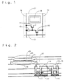
- Fig.1 shows a conventional TFT-OELD.
- Fig. 2 shows a cross-sectional view of a conventional TFT-OELD.
- OELD 18 is a high polymer system, formed by a liquid phase process, such as spin coating, blade coating, ink jet, or the like.
- a gate voltage of a driving TFT 17 is made to change and conductance is changed, so electric current which flows in the OELD 18 needs to be controlled.
- irregularity of transistor characteristics of the driving TFT 17 appears as brightness irregularity of the OELD 18, and there is a problem such that the screen becomes non-uniform.
- a method which implements gradation by changing a light emitting area of the OELD 18 (Japanese Patent Application 9-233107).
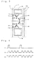
- Fig. 4 shows a driving method of this display.
- a scanning electric potential 31 is applied to a scanning line 12, and a signal line 13 is formed of a signal line (lower bit) 131 and a signal line (upper bit) 132.
- a signal electric potential (lower bit) 321 and signal electric potential (upper bit) 322 are respectively applied as a signal electric potential 32.
- a driving TFT 17 is formed of a driving TFT (lower bit) 171 and a driving TFT (upper bit) 172
- the OELD 18 is formed of an OELD (lower bit) 181 and an OELD (upper bit) 182.
- 2-bit 4 gradation is considered, so an area ratio between OELD (lower bit) 181 and OELD (upper bit) 182 is 1:2.
- the driving TFT 17 takes either a substantially completely on state or a substantially completely off state.
- the resistance of the driving TFT 17 is small enough to be ignored, compared to the resistance of OELD 18, and the electric current amount which flows in the driving TFT 17 and OELD 18 is substantially determined by only the resistance of the OELD 18.
- irregularity of transistor characteristics of the driving TFT 17 does not appear as brightness irregularity of the OELD 18. Furthermore, in the off state, voltage applied to the OELD 18 becomes less than a threshold voltage, so the OELD 18 does not emit light at all, and, needless to say, irregularity of transistor characteristics of the driving TFT 17 does not appear as brightness irregularity of the OELD 18.
- Fig. 5 is a cross-sectional view of TFT-OELD which implements gradation display by changing a light emitting area of the OELD 18 shown in Figs. 3 and 4.
- Fig. 5(a) is a cross-sectional view of the OELD (lower bit) 181
- Fig. 5(b) is a cross-sectional view of the OELD (upper bit) 182.
- the ratio between the light emitting part 25 of the OELD (lower bit) 181 and the light emitting part 25 of the OELD (upper bit) 182 is preferably 1:2.
- a light emitting layer 22 is an OELD of a high polymer system and formed in a liquid phase process.
- a surface of a bank 24 is lyophobic and the light emitting layer 22 does not remain. Therefore, the area of the OELD 18 is determined by patterning. With respect to a side surface of the bank 24, the materials and processing determine whether the side surface of the bank 24 becomes lyophobic or lyophilic.
- Fig. 5 shows the case of a lyophilic side surface of the bank 24.
- the light emitting layer 22 has a cross-sectional shape which is pulled toward the side surface of the bank 24.
- electric current flows into a thinner part of the light emitting layer 22, and this part becomes a light emitting part 25.
- the cross-sectional shape of the light emitting layer 22 described here is sensitive to liquid amount, liquid material, an initial position of the liquid, and a state, temperature, atmosphere, or the like of a substrate, and which are difficult to control. That is, it is difficult to obtain an absolute value of a desired light emitting area.
- Fig. 6 is a cross-sectional view of OELD (lower bit) 181 (Fig. 6(a)) and a cross-sectional view of OELD (upper bit) 182 (Fig. 6 (b)) in the same manner as in Fig. 5.
- the side surface of the bank 24 is lyophobic.
- the light emitting layer 22 has a cross-sectional shape which is distant from the side surface of the bank 24.
- electric current flows into the thinner part of the light emitting layer 22, and this part becomes the light emitting part 25.
- one aspect of this invention is to obtain an accurate ratio of the light emitting parts, and accurate gradation. Therefore, the invention may provide a display device in which gradation is implemented by forming a plurality of TFTs and a plurality of OELDs in each pixel, directly connecting the TFTs and OELDs, switching an on and off state of the TFTs, and controlling an area of the OELDs, that emits light, wherein the plurality of OELDs have the same shape, and gradation is implemented by controlling the number of OELDs that are created to emit light.
- the light emitting part of each OELD is the same area, and accurate gradation can be obtained.
- it is difficult to obtain an absolute value of a desired light emitting area but the light emitting area of a plurality of OELDs becomes equal, so the ratio of the light emitting areas can be accurate by controlling the number OELDs.
- the display device may also include a plurality of OELDs that have a round shape.
- the light emitting part of each OELD can reliably be the same area, and accurate gradation can be obtained.
- the reasons are as follows.
- an OELD has a shape with a rectangular vertex (or vertices)
- a phenomenon may occur, for example, that the vertex becomes pulled in or the vertex cannot be filled. This phenomenon prevents a user from obtaining accurate gradation for the same reason as in the problems of a cross-sectional shape as described above.
- This phenomenon is more sensitive to the liquid amount, liquid material, initial position of liquid, and the state, temperature, and atmosphere of a substrate, more so than the problems in a cross-sectional shape described above, and it is difficult to control this phenomenon between adjacent OELDs. By making the OELD round shaped, this phenomenon can be avoided.
- the display device may also include a plurality of OELDs arranged at the same interval in a horizontal and/or vertical direction. According to this structure, the light emitting part of each OELD is made to be more reliably the same area, and accurate gradation can be obtained.
- the reasons are as follows. When an OELD is formed by spin coating or blade coating, the light emitting layer which is coated over all the pixels, due to the lyophobicity of a surface of the bank, the light emitting layer naturally flows into a convex part of the bank. In the case of ink jet as well, this may sometimes happen.
- OELDs when the OELDs are formed by an ink jet process, ink jetting can be performed at the same interval, so fabrication can be simplified.
- Fig. 7 is a diagram showing a pixel of a TFT-OELD related to a first embodiment of this invention. Here, only one pixel 11 is depicted, but many pixels 11 actually exist in a plurality of rows and a plurality of lines.
- An OELD (lower bit) 181 is formed of OELD (lower bit-rectangular) 1811
- an OELD (upper bit) 182 is formed of OELD (upper bit ⁇ first ⁇ rectangular) 18211 and an OELD (upper bit ⁇ second ⁇ rectangular) 18221.
- the OELD (lower bit ⁇ rectangular) 1811, the OELD (upper bit ⁇ first ⁇ rectangular) 18221, and the OELD (upper bit ⁇ second ⁇ rectangular) 18221 have the same shape, so the same light emitting area can be obtained, and accurate gradation can be obtained by changing the number of OELDs that are caused to emit light.
- Fig. 8 is a diagram showing a pixel of a TFT-OELD related to another embodiment of this invention. Here, only one pixel 11 is depicted, but many pixels 11 actually exist in a plurality of lines and a plurality of rows.
- An OELD (lower bit) 181 is formed of an OELD (lower bit ⁇ round shape) 1812
- an OELD (upper bit) 182 is formed of OELD (upper bit ⁇ first ⁇ round shape) 18212 and OELD (upper bit ⁇ second ⁇ round shape) 18222.
- the OELD (lower bit ⁇ round shape) 1812, the OELD (upper bit ⁇ first ⁇ round shape) 18212, and the OELD (upper bit ⁇ second ⁇ round shape) 18222 have the same round shape, so the same light emitting area can be reliably obtained, and accurate gradation can be obtained.
- Fig. 9 is a diagram showing a pixel of a TFT-OELD related to another embodiment of this invention. Here, only one pixel 11 is depicted, but many pixels 11 actually exist in a plurality of lines and a plurality of rows.
- An OELD (lower bit) 181 is formed of an OELD (lower bit ⁇ round shape) 1812
- an OELD (upper bit) 182 is formed of an OELD (upper bit ⁇ first ⁇ round shape) 18212 and an OELD (upper bit ⁇ second ⁇ round shape) 18222.
- the OELD (lower bit ⁇ round shape) 1812, the OELD (upper bit ⁇ first ⁇ round shape) 18212, and the OELD (upper bit ⁇ second ⁇ round shape) 18222 are arranged at the same interval in horizontal and vertical directions within the pixel 11, and also with respect to the adjacent pixel 11. Because of this, the light emitting part of each OELD can more reliably have the same area, and accurate gradation can be obtained.
- an EL element formed in each pixel in the first embodiment (Fig. 7), a rectangular element is shown as an example, and in the second and third embodiments (Figs. 8 and 9, respectively), a round-shaped element is shown, but this invention is not limited to these. Accurate gradation can also be obtained in a polygonal-or elliptic-shaped element.
- an elliptic element as in the case of a round shape, does not have a vertex such as is present in the case of a rectangular shape, so there is no problem such that the vertex cannot be filled by the light emitting layer.
Landscapes
- Engineering & Computer Science (AREA)
- Physics & Mathematics (AREA)
- Theoretical Computer Science (AREA)
- General Physics & Mathematics (AREA)
- Computer Hardware Design (AREA)
- Geometry (AREA)
- Microelectronics & Electronic Packaging (AREA)
- Signal Processing (AREA)
- Multimedia (AREA)
- Electroluminescent Light Sources (AREA)
- Control Of El Displays (AREA)
- Control Of Indicators Other Than Cathode Ray Tubes (AREA)
- Facsimile Image Signal Circuits (AREA)
- Devices For Indicating Variable Information By Combining Individual Elements (AREA)
Abstract
Description
Claims (9)
- A display device comprising a plurality of pixels, each of the plurality of pixels comprising:a plurality of transistors; anda plurality of organic electro-luminescent elements that have the same emitting area, the plurality of organic electro-luminescent elements being controlled by the plurality of transistors, gradation being obtained by controlling the number of electro-luminescent elements that are caused to emit a light among the plurality of the electro-luminescent elements.
- The display device as set forth in claim 1, wherein the plurality of electro-luminescent elements are round in shape.
- The display device as set forth in claim 1, wherein the plurality of electro-luminescent elements are arranged in at least one direction of the horizontal and vertical directions at equal intervals.
- The display device as set forth in any one of the preceding claims, each of the plurality of electro-luminescent elements being surrounded by a bank.
- The display device as set forth in any one of the preceding claims, wherein there is one transistor among the plurality of transistors that controls two electro-luminescent elements among the plurality of electro-luminescent elements.
- The display device as set forth in any one of the preceding claims, wherein the plurality of electro-luminescent elements are formed by an ink-jet process.
- A method of forming a display device, comprising a step of forming a plurality of organic electro-luminescent elements having the same area by an ink-jet process.
- The method as set forth in claim 7, forming the plurality of organic electro-luminescent elements that are round in shape by the step.
- The method as set forth in claim 7, forming the plurality of organic electro-luminescent elements that are arranged in at least one direction of the horizontal and vertical directions at equal intervals by the step.
Applications Claiming Priority (5)
| Application Number | Priority Date | Filing Date | Title |
|---|---|---|---|
| JP2162399 | 1999-01-29 | ||
| JP2162399 | 1999-01-29 | ||
| JP30144899 | 1999-10-22 | ||
| JP30144899A JP4092827B2 (en) | 1999-01-29 | 1999-10-22 | Display device |
| EP00300329A EP1024472B1 (en) | 1999-01-29 | 2000-01-18 | Organic electroluminescent display device |
Related Parent Applications (1)
| Application Number | Title | Priority Date | Filing Date |
|---|---|---|---|
| EP00300329A Division EP1024472B1 (en) | 1999-01-29 | 2000-01-18 | Organic electroluminescent display device |
Publications (2)
| Publication Number | Publication Date |
|---|---|
| EP1288903A2 true EP1288903A2 (en) | 2003-03-05 |
| EP1288903A3 EP1288903A3 (en) | 2003-06-25 |
Family
ID=26358710
Family Applications (2)
| Application Number | Title | Priority Date | Filing Date |
|---|---|---|---|
| EP00300329A Expired - Lifetime EP1024472B1 (en) | 1999-01-29 | 2000-01-18 | Organic electroluminescent display device |
| EP02079261A Withdrawn EP1288903A3 (en) | 1999-01-29 | 2000-01-18 | Organic electroluminescent display device |
Family Applications Before (1)
| Application Number | Title | Priority Date | Filing Date |
|---|---|---|---|
| EP00300329A Expired - Lifetime EP1024472B1 (en) | 1999-01-29 | 2000-01-18 | Organic electroluminescent display device |
Country Status (7)
| Country | Link |
|---|---|
| US (4) | US6225750B1 (en) |
| EP (2) | EP1024472B1 (en) |
| JP (1) | JP4092827B2 (en) |
| KR (2) | KR100664450B1 (en) |
| CN (1) | CN1123799C (en) |
| DE (1) | DE60004574T2 (en) |
| TW (1) | TW507185B (en) |
Cited By (3)
| Publication number | Priority date | Publication date | Assignee | Title |
|---|---|---|---|---|
| KR100467905B1 (en) * | 1999-01-29 | 2005-01-24 | 세이코 엡슨 가부시키가이샤 | Display device |
| FR2866973A1 (en) * | 2004-02-27 | 2005-09-02 | Commissariat Energie Atomique | Microelectronic device for forming pixels of organic light emission diode type display or screen, has two control units producing currents to control lighting from respective organic light emission type electroluminescent diodes |
| US7633223B2 (en) | 2000-11-10 | 2009-12-15 | Semiconductor Energy Laboratory Co., Ltd. | Organic light emitting device provided with drying agent at side surfaces of a sealing member |
Families Citing this family (64)
| Publication number | Priority date | Publication date | Assignee | Title |
|---|---|---|---|---|
| FR2772501B1 (en) * | 1997-12-15 | 2000-01-21 | Thomson Lcd | MATRIX CONTROL DEVICE |
| JP2000031880A (en) * | 1998-07-16 | 2000-01-28 | Kokusai Electric Co Ltd | Wireless relay device |
| US6366025B1 (en) * | 1999-02-26 | 2002-04-02 | Sanyo Electric Co., Ltd. | Electroluminescence display apparatus |
| KR100430929B1 (en) * | 2000-03-30 | 2004-05-12 | 세이코 엡슨 가부시키가이샤 | Display |
| TW521237B (en) * | 2000-04-18 | 2003-02-21 | Semiconductor Energy Lab | Light emitting device |
| JP2001305998A (en) | 2000-04-25 | 2001-11-02 | Alpine Electronics Inc | Display device |
| US7315295B2 (en) * | 2000-09-29 | 2008-01-01 | Seiko Epson Corporation | Driving method for electro-optical device, electro-optical device, and electronic apparatus |
| JP4632337B2 (en) * | 2000-11-10 | 2011-02-16 | 株式会社半導体エネルギー研究所 | Light emitting device |
| US7071911B2 (en) * | 2000-12-21 | 2006-07-04 | Semiconductor Energy Laboratory Co., Ltd. | Light emitting device, driving method thereof and electric equipment using the light emitting device |
| JP4072332B2 (en) * | 2001-01-09 | 2008-04-09 | シャープ株式会社 | Liquid crystal display device and driving method thereof |
| JP3989718B2 (en) * | 2001-01-18 | 2007-10-10 | シャープ株式会社 | Memory integrated display element |
| JP4051936B2 (en) * | 2001-01-22 | 2008-02-27 | セイコーエプソン株式会社 | Electro-optical device and electronic apparatus |
| JP4777380B2 (en) * | 2001-02-07 | 2011-09-21 | 株式会社半導体エネルギー研究所 | Light emitting device |
| JP4822590B2 (en) * | 2001-02-08 | 2011-11-24 | 三洋電機株式会社 | Organic EL circuit |
| KR100407768B1 (en) * | 2001-07-06 | 2003-12-03 | 주식회사 대한전광 | Display pixel and module for electric signboard using organic electroluminescence |
| US7483001B2 (en) | 2001-11-21 | 2009-01-27 | Seiko Epson Corporation | Active matrix substrate, electro-optical device, and electronic device |
| US6949883B2 (en) | 2001-12-06 | 2005-09-27 | Seiko Epson Corporation | Electro-optical device and an electronic apparatus |
| US6810919B2 (en) * | 2002-01-11 | 2004-11-02 | Seiko Epson Corporation | Manufacturing method for display device, display device, manufacturing method for electronic apparatus, and electronic apparatus |
| US20050180083A1 (en) | 2002-04-26 | 2005-08-18 | Toshiba Matsushita Display Technology Co., Ltd. | Drive circuit for el display panel |
| KR100435054B1 (en) * | 2002-05-03 | 2004-06-07 | 엘지.필립스 엘시디 주식회사 | The organic electro-luminescence device and method for fabricating of the same |
| KR20030086166A (en) * | 2002-05-03 | 2003-11-07 | 엘지.필립스 엘시디 주식회사 | The organic electro-luminescence device and method for fabricating of the same |
| US20040035360A1 (en) * | 2002-05-17 | 2004-02-26 | Semiconductor Energy Laboratory Co., Ltd. | Manufacturing apparatus |
| JP4459521B2 (en) * | 2002-10-17 | 2010-04-28 | 大日本印刷株式会社 | Electroluminescence display device |
| JPWO2004049286A1 (en) * | 2002-11-25 | 2006-03-30 | 東芝松下ディスプレイテクノロジー株式会社 | Organic EL display panel |
| KR101179155B1 (en) * | 2002-12-27 | 2012-09-07 | 가부시키가이샤 한도오따이 에네루기 켄큐쇼 | Display device |
| JP2004220021A (en) * | 2002-12-27 | 2004-08-05 | Semiconductor Energy Lab Co Ltd | Display device |
| JP4619289B2 (en) | 2003-03-26 | 2011-01-26 | 株式会社半導体エネルギー研究所 | Display device, driving method thereof, and electronic apparatus |
| CN100380596C (en) * | 2003-04-25 | 2008-04-09 | 株式会社半导体能源研究所 | Droplet discharge device, pattern forming method, and semiconductor device manufacturing method |
| US6771028B1 (en) * | 2003-04-30 | 2004-08-03 | Eastman Kodak Company | Drive circuitry for four-color organic light-emitting device |
| US20040257352A1 (en) * | 2003-06-18 | 2004-12-23 | Nuelight Corporation | Method and apparatus for controlling |
| TWI366701B (en) * | 2004-01-26 | 2012-06-21 | Semiconductor Energy Lab | Method of manufacturing display and television |
| US7273773B2 (en) * | 2004-01-26 | 2007-09-25 | Semiconductor Energy Laboratory Co., Ltd. | Display device, method for manufacturing thereof, and television device |
| US20060007248A1 (en) * | 2004-06-29 | 2006-01-12 | Damoder Reddy | Feedback control system and method for operating a high-performance stabilized active-matrix emissive display |
| US20050200294A1 (en) * | 2004-02-24 | 2005-09-15 | Naugler W. E.Jr. | Sidelight illuminated flat panel display and touch panel input device |
| JP4466115B2 (en) * | 2004-02-24 | 2010-05-26 | セイコーエプソン株式会社 | ORGANIC ELECTROLUMINESCENT DEVICE, METHOD FOR PRODUCING ORGANIC ELECTROLUMINESCENT DEVICE, AND ELECTRONIC DEVICE |
| US20050200292A1 (en) * | 2004-02-24 | 2005-09-15 | Naugler W. E.Jr. | Emissive display device having sensing for luminance stabilization and user light or touch screen input |
| US20050200296A1 (en) * | 2004-02-24 | 2005-09-15 | Naugler W. E.Jr. | Method and device for flat panel emissive display using shielded or partially shielded sensors to detect user screen inputs |
| US7462514B2 (en) | 2004-03-03 | 2008-12-09 | Semiconductor Energy Laboratory Co., Ltd. | Semiconductor device and method for manufacturing the same, liquid crystal television, and EL television |
| US7642038B2 (en) | 2004-03-24 | 2010-01-05 | Semiconductor Energy Laboratory Co., Ltd. | Method for forming pattern, thin film transistor, display device, method for manufacturing thereof, and television apparatus |
| US20050243023A1 (en) * | 2004-04-06 | 2005-11-03 | Damoder Reddy | Color filter integrated with sensor array for flat panel display |
| CN1981318A (en) * | 2004-04-12 | 2007-06-13 | 彩光公司 | Low power circuits for active matrix emissive displays and methods of operating the same |
| US20050248515A1 (en) * | 2004-04-28 | 2005-11-10 | Naugler W E Jr | Stabilized active matrix emissive display |
| US7199397B2 (en) * | 2004-05-05 | 2007-04-03 | Au Optronics Corporation | AMOLED circuit layout |
| KR101043394B1 (en) * | 2004-05-14 | 2011-06-22 | 삼성전자주식회사 | Chemical Formation Apparatus and Method |
| US8158517B2 (en) * | 2004-06-28 | 2012-04-17 | Semiconductor Energy Laboratory Co., Ltd. | Method for manufacturing wiring substrate, thin film transistor, display device and television device |
| JP2006065284A (en) | 2004-07-26 | 2006-03-09 | Seiko Epson Corp | LIGHT EMITTING DEVICE AND ELECTRONIC DEVICE |
| CN101251986B (en) * | 2004-07-26 | 2012-01-04 | 精工爱普生株式会社 | Light-emitting device |
| KR100699997B1 (en) * | 2004-09-21 | 2007-03-26 | 삼성에스디아이 주식회사 | An organic light emitting display device having a plurality of driving transistors and a plurality of anode or cathode electrodes |
| US20070001954A1 (en) * | 2005-07-04 | 2007-01-04 | Semiconductor Energy Laboratory Co., Ltd. | Display device and driving method of display device |
| KR100729077B1 (en) * | 2005-11-14 | 2007-06-14 | 삼성에스디아이 주식회사 | Organic light emitting display |
| KR100688971B1 (en) * | 2006-02-16 | 2007-03-08 | 삼성전자주식회사 | Display device |
| KR101304837B1 (en) * | 2006-12-29 | 2013-09-05 | 엘지전자 주식회사 | A power saving display system for refrigerator |
| JP2008180802A (en) * | 2007-01-23 | 2008-08-07 | Eastman Kodak Co | Active matrix display device |
| JP5242076B2 (en) * | 2007-04-13 | 2013-07-24 | グローバル・オーエルイーディー・テクノロジー・リミテッド・ライアビリティ・カンパニー | Active matrix display device |
| WO2009113239A1 (en) * | 2008-03-13 | 2009-09-17 | パナソニック株式会社 | Organic el display panel and manufacturing method thereof |
| TWI411992B (en) * | 2010-12-14 | 2013-10-11 | Au Optronics Corp | Driving method of display apparatus and display apparatus |
| CN103489401B (en) * | 2013-09-03 | 2016-11-23 | 京东方科技集团股份有限公司 | Image element circuit and driving method, array base palte and display device |
| US9806098B2 (en) | 2013-12-10 | 2017-10-31 | Semiconductor Energy Laboratory Co., Ltd. | Light-emitting device |
| JP2016042195A (en) * | 2015-11-12 | 2016-03-31 | 株式会社半導体エネルギー研究所 | Display device |
| KR102490894B1 (en) | 2018-02-08 | 2023-01-25 | 삼성디스플레이 주식회사 | Organic light emitting display apparatus |
| CN110021260B (en) * | 2018-06-27 | 2021-01-26 | 京东方科技集团股份有限公司 | Pixel circuit, driving method thereof and display device |
| US20220352481A1 (en) * | 2019-10-08 | 2022-11-03 | Sharp Kabushiki Kaisha | Light-emitting device |
| CN111769143B (en) * | 2020-06-23 | 2022-09-09 | 武汉华星光电半导体显示技术有限公司 | Display panel and manufacturing method thereof |
| US12183280B2 (en) * | 2021-07-01 | 2024-12-31 | Universal Display Corporation | Means to reduce OLED transient response |
Family Cites Families (12)
| Publication number | Priority date | Publication date | Assignee | Title |
|---|---|---|---|---|
| JPS5688193A (en) * | 1979-12-19 | 1981-07-17 | Citizen Watch Co Ltd | Display unit |
| JPS6122326A (en) * | 1984-03-23 | 1986-01-30 | Citizen Watch Co Ltd | Gradational display device |
| US5459678A (en) * | 1992-07-02 | 1995-10-17 | Feasey; Michael F. | Method and calibration apparatus for calibrating computer monitors used in the printing and textile industries |
| US5714968A (en) * | 1994-08-09 | 1998-02-03 | Nec Corporation | Current-dependent light-emitting element drive circuit for use in active matrix display device |
| US5732151A (en) * | 1995-03-03 | 1998-03-24 | Hewlett-Packard Company | Computerized memory mapping method for transforming color data |
| US5585695A (en) * | 1995-06-02 | 1996-12-17 | Adrian Kitai | Thin film electroluminescent display module |
| US5834894A (en) * | 1995-09-14 | 1998-11-10 | Casio Computer Co., Ltd. | Carrier injection type organic electro-luminescent device which emits light in response to an application of a voltage |
| WO1997024907A1 (en) * | 1995-12-30 | 1997-07-10 | Casio Computer Co., Ltd. | Display device for performing display operation in accordance with signal light and driving method therefor |
| DE69825402T2 (en) * | 1997-03-12 | 2005-08-04 | Seiko Epson Corp. | PIXEL CIRCUIT, DISPLAY DEVICE AND ELECTRONIC APPARATUS WITH POWER-CONTROLLED LIGHT-EMITTING DEVICE |
| JPH1173158A (en) | 1997-08-28 | 1999-03-16 | Seiko Epson Corp | Display element |
| JP2000058270A (en) * | 1998-08-04 | 2000-02-25 | Sony Corp | Optical element and organic EL display |
| JP4092827B2 (en) * | 1999-01-29 | 2008-05-28 | セイコーエプソン株式会社 | Display device |
-
1999
- 1999-10-22 JP JP30144899A patent/JP4092827B2/en not_active Expired - Lifetime
- 1999-12-07 KR KR1019990055506A patent/KR100664450B1/en not_active Expired - Fee Related
- 1999-12-21 US US09/468,356 patent/US6225750B1/en not_active Expired - Lifetime
- 1999-12-27 TW TW088123045A patent/TW507185B/en not_active IP Right Cessation
-
2000
- 2000-01-18 EP EP00300329A patent/EP1024472B1/en not_active Expired - Lifetime
- 2000-01-18 DE DE60004574T patent/DE60004574T2/en not_active Expired - Lifetime
- 2000-01-18 EP EP02079261A patent/EP1288903A3/en not_active Withdrawn
- 2000-01-27 KR KR10-2000-0003881A patent/KR100467905B1/en not_active Expired - Lifetime
- 2000-01-28 CN CN00101923A patent/CN1123799C/en not_active Expired - Lifetime
-
2001
- 2001-03-30 US US09/820,763 patent/US6388389B2/en not_active Expired - Lifetime
-
2002
- 2002-04-02 US US10/112,710 patent/US6469450B2/en not_active Expired - Lifetime
- 2002-09-04 US US10/233,402 patent/US6642665B2/en not_active Expired - Lifetime
Cited By (5)
| Publication number | Priority date | Publication date | Assignee | Title |
|---|---|---|---|---|
| KR100467905B1 (en) * | 1999-01-29 | 2005-01-24 | 세이코 엡슨 가부시키가이샤 | Display device |
| US7633223B2 (en) | 2000-11-10 | 2009-12-15 | Semiconductor Energy Laboratory Co., Ltd. | Organic light emitting device provided with drying agent at side surfaces of a sealing member |
| FR2866973A1 (en) * | 2004-02-27 | 2005-09-02 | Commissariat Energie Atomique | Microelectronic device for forming pixels of organic light emission diode type display or screen, has two control units producing currents to control lighting from respective organic light emission type electroluminescent diodes |
| WO2005086130A1 (en) * | 2004-02-27 | 2005-09-15 | Commissariat A L'energie Atomique | Device for improving pixel addressing |
| US7554533B2 (en) | 2004-02-27 | 2009-06-30 | Commissariat A L'energie Atomique | Device for improving pixel addressing |
Also Published As
| Publication number | Publication date |
|---|---|
| JP4092827B2 (en) | 2008-05-28 |
| US20020105280A1 (en) | 2002-08-08 |
| CN1123799C (en) | 2003-10-08 |
| JP2000284727A (en) | 2000-10-13 |
| KR100467905B1 (en) | 2005-01-24 |
| US6388389B2 (en) | 2002-05-14 |
| US6642665B2 (en) | 2003-11-04 |
| US20020195969A1 (en) | 2002-12-26 |
| DE60004574D1 (en) | 2003-09-25 |
| KR100664450B1 (en) | 2007-01-04 |
| US6469450B2 (en) | 2002-10-22 |
| KR20000053629A (en) | 2000-08-25 |
| EP1024472A3 (en) | 2000-11-15 |
| US20020011793A1 (en) | 2002-01-31 |
| CN1263279A (en) | 2000-08-16 |
| US6225750B1 (en) | 2001-05-01 |
| DE60004574T2 (en) | 2004-02-26 |
| TW507185B (en) | 2002-10-21 |
| KR20000052429A (en) | 2000-08-25 |
| EP1288903A3 (en) | 2003-06-25 |
| EP1024472A2 (en) | 2000-08-02 |
| EP1024472B1 (en) | 2003-08-20 |
Similar Documents
| Publication | Publication Date | Title |
|---|---|---|
| US6225750B1 (en) | Display device | |
| US6734505B2 (en) | Thin film transistor and use of same | |
| KR102665322B1 (en) | Thin film transistor substrate, and display apparatus | |
| KR100533455B1 (en) | Light-emitting apparatus and method of producing the same | |
| KR100743948B1 (en) | Organic EL and optical devices | |
| JP3946663B2 (en) | Active organic electroluminescence device and manufacturing method thereof | |
| JP2004126439A (en) | Electro-optical device, matrix substrate, and electronic equipment | |
| US6459208B2 (en) | Active matrix electroluminescent display device | |
| KR20140086439A (en) | Organic light emitting device | |
| JP4451779B2 (en) | Electroluminescent display device | |
| KR100686343B1 (en) | Organic electroluminescent display | |
| US8427049B2 (en) | Display device | |
| JP4192879B2 (en) | Display panel | |
| KR100684825B1 (en) | Organic electroluminescence display device and manufacturing method thereof | |
| JP2002299049A (en) | Organic electroluminescence unit | |
| KR100550005B1 (en) | Surface-emitting organic EL diode display device and manufacturing method thereof | |
| KR101294843B1 (en) | Light Emitting Diodes and Method of Manufacturing for the same | |
| KR20040087427A (en) | Organic electro-luminescent panel and organic electro-luminescent display device | |
| JP2006098723A (en) | Display panel |
Legal Events
| Date | Code | Title | Description |
|---|---|---|---|
| PUAI | Public reference made under article 153(3) epc to a published international application that has entered the european phase |
Free format text: ORIGINAL CODE: 0009012 |
|
| 17P | Request for examination filed |
Effective date: 20021105 |
|
| AC | Divisional application: reference to earlier application |
Ref document number: 1024472 Country of ref document: EP Kind code of ref document: P |
|
| AK | Designated contracting states |
Designated state(s): DE FI FR GB NL Kind code of ref document: A2 Designated state(s): DE FI FR GB NL |
|
| PUAL | Search report despatched |
Free format text: ORIGINAL CODE: 0009013 |
|
| AK | Designated contracting states |
Designated state(s): DE FI FR GB NL |
|
| AKX | Designation fees paid |
Designated state(s): DE FI FR GB NL |
|
| 17Q | First examination report despatched |
Effective date: 20070814 |
|
| STAA | Information on the status of an ep patent application or granted ep patent |
Free format text: STATUS: THE APPLICATION IS DEEMED TO BE WITHDRAWN |
|
| 18D | Application deemed to be withdrawn |
Effective date: 20100803 |