EP1288900A1 - Active matrix display device and mobile terminal using the device - Google Patents
Active matrix display device and mobile terminal using the device Download PDFInfo
- Publication number
- EP1288900A1 EP1288900A1 EP01999935A EP01999935A EP1288900A1 EP 1288900 A1 EP1288900 A1 EP 1288900A1 EP 01999935 A EP01999935 A EP 01999935A EP 01999935 A EP01999935 A EP 01999935A EP 1288900 A1 EP1288900 A1 EP 1288900A1
- Authority
- EP
- European Patent Office
- Prior art keywords
- circuit
- display apparatus
- set forth
- active matrix
- matrix type
- Prior art date
- Legal status (The legal status is an assumption and is not a legal conclusion. Google has not performed a legal analysis and makes no representation as to the accuracy of the status listed.)
- Granted
Links
Images




Classifications
-
- G—PHYSICS
- G02—OPTICS
- G02F—OPTICAL DEVICES OR ARRANGEMENTS FOR THE CONTROL OF LIGHT BY MODIFICATION OF THE OPTICAL PROPERTIES OF THE MEDIA OF THE ELEMENTS INVOLVED THEREIN; NON-LINEAR OPTICS; FREQUENCY-CHANGING OF LIGHT; OPTICAL LOGIC ELEMENTS; OPTICAL ANALOGUE/DIGITAL CONVERTERS
- G02F1/00—Devices or arrangements for the control of the intensity, colour, phase, polarisation or direction of light arriving from an independent light source, e.g. switching, gating or modulating; Non-linear optics
- G02F1/01—Devices or arrangements for the control of the intensity, colour, phase, polarisation or direction of light arriving from an independent light source, e.g. switching, gating or modulating; Non-linear optics for the control of the intensity, phase, polarisation or colour
- G02F1/13—Devices or arrangements for the control of the intensity, colour, phase, polarisation or direction of light arriving from an independent light source, e.g. switching, gating or modulating; Non-linear optics for the control of the intensity, phase, polarisation or colour based on liquid crystals, e.g. single liquid crystal display cells
- G02F1/133—Constructional arrangements; Operation of liquid crystal cells; Circuit arrangements
-
- G—PHYSICS
- G09—EDUCATION; CRYPTOGRAPHY; DISPLAY; ADVERTISING; SEALS
- G09G—ARRANGEMENTS OR CIRCUITS FOR CONTROL OF INDICATING DEVICES USING STATIC MEANS TO PRESENT VARIABLE INFORMATION
- G09G3/00—Control arrangements or circuits, of interest only in connection with visual indicators other than cathode-ray tubes
- G09G3/20—Control arrangements or circuits, of interest only in connection with visual indicators other than cathode-ray tubes for presentation of an assembly of a number of characters, e.g. a page, by composing the assembly by combination of individual elements arranged in a matrix no fixed position being assigned to or needed to be assigned to the individual characters or partial characters
- G09G3/2007—Display of intermediate tones
- G09G3/2011—Display of intermediate tones by amplitude modulation
-
- G—PHYSICS
- G09—EDUCATION; CRYPTOGRAPHY; DISPLAY; ADVERTISING; SEALS
- G09G—ARRANGEMENTS OR CIRCUITS FOR CONTROL OF INDICATING DEVICES USING STATIC MEANS TO PRESENT VARIABLE INFORMATION
- G09G3/00—Control arrangements or circuits, of interest only in connection with visual indicators other than cathode-ray tubes
- G09G3/20—Control arrangements or circuits, of interest only in connection with visual indicators other than cathode-ray tubes for presentation of an assembly of a number of characters, e.g. a page, by composing the assembly by combination of individual elements arranged in a matrix no fixed position being assigned to or needed to be assigned to the individual characters or partial characters
- G09G3/34—Control arrangements or circuits, of interest only in connection with visual indicators other than cathode-ray tubes for presentation of an assembly of a number of characters, e.g. a page, by composing the assembly by combination of individual elements arranged in a matrix no fixed position being assigned to or needed to be assigned to the individual characters or partial characters by control of light from an independent source
- G09G3/36—Control arrangements or circuits, of interest only in connection with visual indicators other than cathode-ray tubes for presentation of an assembly of a number of characters, e.g. a page, by composing the assembly by combination of individual elements arranged in a matrix no fixed position being assigned to or needed to be assigned to the individual characters or partial characters by control of light from an independent source using liquid crystals
- G09G3/3611—Control of matrices with row and column drivers
- G09G3/3685—Details of drivers for data electrodes
- G09G3/3688—Details of drivers for data electrodes suitable for active matrices only
-
- G—PHYSICS
- G09—EDUCATION; CRYPTOGRAPHY; DISPLAY; ADVERTISING; SEALS
- G09G—ARRANGEMENTS OR CIRCUITS FOR CONTROL OF INDICATING DEVICES USING STATIC MEANS TO PRESENT VARIABLE INFORMATION
- G09G3/00—Control arrangements or circuits, of interest only in connection with visual indicators other than cathode-ray tubes
- G09G3/20—Control arrangements or circuits, of interest only in connection with visual indicators other than cathode-ray tubes for presentation of an assembly of a number of characters, e.g. a page, by composing the assembly by combination of individual elements arranged in a matrix no fixed position being assigned to or needed to be assigned to the individual characters or partial characters
- G09G3/34—Control arrangements or circuits, of interest only in connection with visual indicators other than cathode-ray tubes for presentation of an assembly of a number of characters, e.g. a page, by composing the assembly by combination of individual elements arranged in a matrix no fixed position being assigned to or needed to be assigned to the individual characters or partial characters by control of light from an independent source
- G09G3/36—Control arrangements or circuits, of interest only in connection with visual indicators other than cathode-ray tubes for presentation of an assembly of a number of characters, e.g. a page, by composing the assembly by combination of individual elements arranged in a matrix no fixed position being assigned to or needed to be assigned to the individual characters or partial characters by control of light from an independent source using liquid crystals
- G09G3/3611—Control of matrices with row and column drivers
- G09G3/3696—Generation of voltages supplied to electrode drivers
-
- G—PHYSICS
- G09—EDUCATION; CRYPTOGRAPHY; DISPLAY; ADVERTISING; SEALS
- G09G—ARRANGEMENTS OR CIRCUITS FOR CONTROL OF INDICATING DEVICES USING STATIC MEANS TO PRESENT VARIABLE INFORMATION
- G09G2300/00—Aspects of the constitution of display devices
- G09G2300/04—Structural and physical details of display devices
- G09G2300/0404—Matrix technologies
- G09G2300/0408—Integration of the drivers onto the display substrate
-
- G—PHYSICS
- G09—EDUCATION; CRYPTOGRAPHY; DISPLAY; ADVERTISING; SEALS
- G09G—ARRANGEMENTS OR CIRCUITS FOR CONTROL OF INDICATING DEVICES USING STATIC MEANS TO PRESENT VARIABLE INFORMATION
- G09G2300/00—Aspects of the constitution of display devices
- G09G2300/08—Active matrix structure, i.e. with use of active elements, inclusive of non-linear two terminal elements, in the pixels together with light emitting or modulating elements
-
- G—PHYSICS
- G09—EDUCATION; CRYPTOGRAPHY; DISPLAY; ADVERTISING; SEALS
- G09G—ARRANGEMENTS OR CIRCUITS FOR CONTROL OF INDICATING DEVICES USING STATIC MEANS TO PRESENT VARIABLE INFORMATION
- G09G2310/00—Command of the display device
- G09G2310/06—Details of flat display driving waveforms
-
- G—PHYSICS
- G09—EDUCATION; CRYPTOGRAPHY; DISPLAY; ADVERTISING; SEALS
- G09G—ARRANGEMENTS OR CIRCUITS FOR CONTROL OF INDICATING DEVICES USING STATIC MEANS TO PRESENT VARIABLE INFORMATION
- G09G2330/00—Aspects of power supply; Aspects of display protection and defect management
- G09G2330/02—Details of power systems and of start or stop of display operation
-
- G—PHYSICS
- G09—EDUCATION; CRYPTOGRAPHY; DISPLAY; ADVERTISING; SEALS
- G09G—ARRANGEMENTS OR CIRCUITS FOR CONTROL OF INDICATING DEVICES USING STATIC MEANS TO PRESENT VARIABLE INFORMATION
- G09G2330/00—Aspects of power supply; Aspects of display protection and defect management
- G09G2330/02—Details of power systems and of start or stop of display operation
- G09G2330/021—Power management, e.g. power saving
Definitions
- This invention relates to an active matrix type display apparatus and a portable terminal using the same, and more particularly to an active matrix type display apparatus wherein a polycrystalline silicon TFT (Thin Film Transistor) is used as a switching element of a pixel and a portable terminal wherein the active matrix type display apparatus is used as a display section.
- a polycrystalline silicon TFT Thin Film Transistor
- liquid crystal display apparatus incorporated as an output display section of the portable terminals.
- the liquid crystal display apparatus has a characteristic that power for driving the same is not required in principle and is a display device of low power consumption.
- a demand for further reduction of power consumption of a display apparatus is increasing as such rapid popularization of portable terminals.
- Reduction of the power consumption particularly within a standby period is a significant point for increasing the duration of a battery, and therefore, this is one of the items for which the demand is strong.
- Various power saving techniques have been proposed to satisfy the demand.
- One of such techniques is the 1-bit mode (two-gradation mode) which restricts the number of gradations of a display of an image in a standby state to "2" (1 bit) for each color.
- a gradation is represented with 1 bit for each color, and therefore, an image is displayed using totaling eight colors.
- a number of analog circuits equal to the number of outputs are disposed in an output section of a data line driving circuit (horizontal driving circuit). Since fixed bias current must always be supplied to the buffer circuits, the buffer circuits make a major factor which consumes such a high power.
- the data line driving circuit of the amorphous silicon TFT liquid crystal display apparatus conventionally adopts a configuration that, in order to allow the same to deal with the 1-bit mode described above, a CMOS inverter is connected in parallel to each of the buffer circuits of the output section and is used in place of the buffer circuit when the gradation number is to be restricted to "2" as a result of setting of the 1-bit mode. Since no DC current may be supplied to the CMOS inverter and therefore the DC current to the output section of the data line driving circuit can be reduced significantly, reduction of the power consumption can be achieved.
- a liquid crystal active matrix type display apparatus wherein a polycrystalline silicon TFT is used as a switching element of a pixel in recent years, there is a tendency to form a digital interface driving circuit integrally on the same substrate as that of a display area section on which pixels are arranged in a matrix manner.
- a horizontal driving system and a vertical driving system are disposed at peripheral portions (a frame) of the display area section and are formed integrally on the same substrate as that of the pixel area section using a polycrystalline silicon TFT.
- the present invention has been made in view of the subject described above, and it is an object of the present invention to provide an active matrix type display apparatus to which reduction of the power consumption by the 1-bit mode can be applied while it uses a polycrystalline silicon TFT structure of the driving circuit integration type thereby to achieve further reduction of the power consumption and a portable terminal wherein the active matrix type display apparatus is used as a display section.
- an active matrix type display apparatus which includes a display area section wherein pixels each having an electro-optical device are disposed in a matrix manner, a vertical driving circuit for selecting the pixels of the display area section in a unit of a row, and a horizontal driving circuit for receiving digital image data as an input thereto and supplying the digital image data as an analog image signal to the pixels of a row selected by the vertical driving circuit is configured such that, when a low gradation mode which uses a smaller number of gradations than a normal mode is set, only a number of circuit portions of the horizontal driving circuit equal to the number of gradations are placed into an active state.
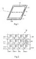
- FIG. 1 is a view of a schematic configuration showing an example of a configuration of a display apparatus according to the present invention.
- description is given taking, as an example, a case wherein the present invention is applied, for example, to a liquid crystal active matrix type display apparatus in which a liquid crystal cell is incorporated as an electro-optical element of each pixel.
- a display area section 12 wherein a large number of pixels each including a liquid crystal cell are disposed in a matrix manner, a pair of upper and lower H drivers (horizontal driving circuits) 13U and 13D and a V driver (vertical driving circuit) 14 as well as a reference voltage generation circuit 15 for generating a plurality of reference voltages and a 1-bit mode control circuit 16 are integrated on a transparent insulation substrate, for example, a glass substrate 11.
- the glass substrate 11 is formed from a first substrate wherein a large number of pixel circuits each including an active device (for example, a transistor) are disposed in a matrix manner and a second substrate disposed in an opposing relationship to the first substrate with a predetermined gap left therebetween.
- a liquid crystal material is enclosed in a space between the first and second substrates.
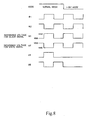
- FIG. 2 An example of a particular configuration of the display area section 12 is shown in FIG. 2.
- a pixel arrangement of three rows (n-1th row to n+1th row) and four columns (m-2th column to m+1th column) is shown as an example.
- vertical scanning lines ⁇ , 21n-1, 21n, 21n+1, ⁇ , and data lines ⁇ , 22m-2, 22m-1, 22m, 22m+1, ⁇ are wired in a matrix manner on the display area section 12, and a unit pixel 23 is disposed at each of intersection points of the vertical scanning lines and the data lines.
- the unit pixel 23 includes a thin film transistor TFT which is a pixel transistor, a liquid crystal cell LC and a storage capacitor Cs.
- the liquid crystal cell LC signifies a capacitor which is produced between a pixel electrode (one electrode) formed from the thin film transistor TFT and a counter-electrode (the other electrode) formed in an opposing relationship to the pixel electrode.
- the gate electrode of the thin film transistor TFT is connected to the vertical scanning lines ⁇ , , 21n-1, 21n, 21n+1, ⁇ , and the source electrode of the thin film transistor TFT is connected to the data lines ⁇ , 22m-2, 22m-1, 22m, 22m+1, ⁇ .
- the pixel electrode of the liquid crystal cell LC is connected to the drain electrode of the thin film transistor TFT and the counter-electrode of the liquid crystal cell LC is connected to a common line 24.
- the storage capacitor Cs is connected between the drain electrode of the thin film transistor TFT and the common line 24.
- a predetermined DC voltage is applied as a common voltage Vcom to the common line 24.
- each of the vertical scanning lines ⁇ , 21n-1, 21n, 21n+1, ⁇ is connected to an output terminal of the V driver 14 shown in FIG. 1 for a corresponding one of the rows.
- the V driver 14 is formed from, for example, a shift register, and successively generates a vertical selection pulse in synchronism with a vertical transfer clock VCK (not shown) and applies it to the vertical scanning lines ⁇ , 21n-1, 21n, 21n+1, ⁇ to perform vertical scanning.
- one terminal of each of the data lines of odd numbers ⁇ , 21n-1, 21n+1, ⁇ is connected to an output terminal of the H driver 13U shown in FIG. 1 for a corresponding one of the columns and each of the other terminals of the data lines of even numbers ⁇ , 22m-2, 22m, ⁇ is connected to an output terminal of the H driver 13D shown in FIG. 1 for a corresponding one of the columns.
- FIG. 3 is a block diagram particularly showing a mutual relationship of different components on the glass substrate 11.
- the H driver 13U on the upper side is shown for simplification of the drawing.
- the H driver 13D on the lower side has a quite similar configuration to that to the H driver 13U.
- the liquid crystal active matrix type display apparatus according to the present example adopts the configuration wherein the H drivers 13U and 13D are disposed above on the upper and lower sides of the display area section 12, the configuration is not limited to this, and it is otherwise possible to adopt another configuration wherein the H drives 13U and 13D are disposed on only one of the upper and lower sides of the display area section 12.
- the H driver 13U includes a shift register 25U, a sampling latch circuit (data signal inputting circuit) 26U, a line sequence latch circuit 27U, and a D/A conversion circuit 28U.
- the shift resister 25U sequentially outputs a shift pulse from each transfer stage thereof in synchronism with a horizontal transfer clock HCK (not shown) to perform horizontal scanning.
- the sampling latch circuit 26U samples and latches, in point sequence, digital image data of predetermined bits inputted in response to the shift pulse supplied thereto from the shift register 25U to latch the digital image data.
- the line sequence latch circuit 27U latches the digital image data latched in point sequence by the sampling latch circuit 26U in a unit of one line again to perform line sequence of the digital image data, and outputs the digital image data for one line at a time.
- the D/A conversion circuit 28U has a configuration of, for example, a circuit of the reference voltage selection type, and converts the digital image data for one line outputted from the line sequence latch circuit 27U into an analog image signal and supplies it to the data lines ⁇ , 22m-2, 22m-1, 22m, 22m+1, ⁇ of the pixel area section 12.
- the reference voltage generation circuit 15 is a circuit attendant on the reference voltage selection type D/A conversion circuit 28U, and generates a number of reference voltages equal to the number of gradations corresponding to the bit number of input image data and applies the reference voltages to the reference voltage selection type D/A conversion circuit 28U.
- the 1-bit mode control circuit 16 performs control of the horizontal driving system (H drivers 13U and 13D) including the reference voltage generation circuit 15 to render only a number of circuit portions equal to the number of gradations (in the present example, 2 gradations) into an active state when a low gradation mode which is one of the power saving modes, for example, a 2-gradation mode (1-bit mode) is designated.
- the reference voltage generation circuit 15 and the 1-bit mode control circuit 16 are formed integrally on the same glass substrate 11 together with the display area section 12, for example, in the case of a liquid crystal active matrix type display apparatus which adopts the configuration wherein the H drivers 13U and 13D are disposed on the upper and lower sides of the display area section 12, preferably the reference voltage generation circuit 15 and the 1-bit mode control circuit 16 are disposed in a frame area (peripheral area of the display area section 12) on a side or sides on which the H drivers 13U and 13D are not incorporated.
- the H drivers 13U and 13D include a great number of components when compared with the V driver 14 as described above and in most cases have a very great circuit area, where they are disposed in the frame area on a side or sides on which the H drivers 13U and 13D are not disposed, the reference voltage generation circuit 15 and the 1-bit mode control circuit 16 can be integrated on the same glass substrate 11 as that of the display area section 12 without deteriorating the effective screen ratio (the area ratio of the display area section 12 to the glass substrate 11).
- the liquid crystal active matrix type display apparatus adopts the configuration wherein, since the V driver 14 is mounted on one side of the frame area on one of the two sides on which the H drivers 13U and 13D are not disposed, the reference voltage generation circuit 15 and the 1-bit mode control circuit 16 are integrated in the frame area on another side on which the H drivers 13U and 13D are not disposed.
- H drivers 13U and 13D, V driver 14, reference voltage generation circuit 15 and 1-bit mode control circuit 16 since a polycrystalline silicon thin film transistor TFT is used for the pixel transistors of the display area section 12, if a polycrystalline silicon thin film transistor is used also for the transistors which form the components mentioned and at least the transistor circuits of the same are produced on the same glass substrate 11 together with the display area section 12, then they can be produced readily and besides can be implemented at a low cost.
- the thin film transistor TFT As things stand, integration has become easy thanks to the augmentation in performance and reduction of the power consumption in recent years. Accordingly, where the H drivers 13U and 13D, V driver 14, reference voltage generation circuit 15 and 1-bit mode control circuit 16, particularly at least transistor circuits of components of them, are formed integrally on the same glass substrate 11 by the same process using a thin film transistor same as that used for the pixel transistors of the display area section 12, reduction of the cost by simplification of the production process and besides reduction in thickness and compaction by integration can be achieved.
- FIG. 4 is a block diagram showing a particular example of a configuration of the sampling latch circuit 26U.
- three AND circuits 31-0, 31-1 and 31-2 are provided corresponding to the transfer stage 25Uk of the kth stage of the shift register 25U and three AND circuits 32-0, 32-1 and 32-2 are provided corresponding to the transfer stage 25Uk+1 of the k+1th stage of the shift register 25U.
- the number of the AND circuits is a number corresponding to the bit number "3" of the digital image data.
- Shift pulses of the transfer stages 25Uk and 25Uk+1 of the shift register 25U are applied as sampling pulses SPk and SPk+1 to input terminals of the AND circuits 31-0, 31-1, 31-2, 32-0, 32-1 and 32-2 on one side.
- a control signal A is applied to the other input terminals of the AND circuits 31-2 and 32-2 from the 1-bit mode control circuit 16 over a control line 33A.
- a control signal B is applied to the other input terminals of the AND circuits 31-0, 31-1, 32-0 and 32-1 from the 1-bit mode control circuit 16 over a control line 33B.
- sampling latch circuit 26U digital image data of, for example, 3 bits is inputted over bit lines 34-0, 34-1 and 34-2.
- Latch circuits 35-0, 35-1 and 35-2 and latch circuits 36-0, 36-1 and 36-2 are provided for latching the digital image data of 3 bits in response to the sampling pulses SPk and SPk+1 outputted successively from the transfer stages 25Uk and 25Uk+1 of the shift register 25U.
- Switches 37-0, 37-1 and 37-2 are connected between the input terminals of the latch circuits 35-0, 35-1 and 35-2 and the bit lines 34-0, 34-1 and 34-2, and switches 38-0, 38-1 and 38-2 are connected between the input terminals of the latch circuits 36-0, 36-1 and 36-2 and the bit lines 34-0, 34-1 and 34-2.
- the switches 37-0, 37-1, 37-2, 38-0, 38-1 and 38-2 are controlled between on (close)/off (open) with outputs of the AND circuits 31-0, 31-1, 31-2, 32-0, 32-1 and 32-2, respectively.
- the control signals A and B both having the "H" level (high level) are outputted from the 1-bit mode control circuit 16. Consequently, the sampling pulses SPk and SPk+1 successively outputted from the transfer stages 25Uk and 25Uk+1 of the shift register 25U are supplied to all of the switches 37-0, 37-1, 37-2, 38-0, 38-1 and 38-2 through the AND circuits 31-0 to 31-2 and 32-0 to 32-2, respectively. As a result, all of the latch circuits 35-0 to 35-2 and 36-0 to 36-2 are placed into an active state, that is, into a state wherein data can be written into (latched by) them.
- the control signal A of the "H” level and the control signal B of the "L” level (low level) are outputted from the 1-bit mode control circuit 16. Consequently, since only the AND circuits 31-2 and 32-2 corresponding to the most significant bit (MSB) are placed into a passage permitting state, the sampling pulses SPk and SPk+1 successively outputted from the transfer stages 25Uk and 25Uk+1 of the shift register 25U are supplied only to the switches 37-2 and 38-2 through the AND circuits 31-2 and 32-2, respectively.
- FIG. 5 is a block diagram showing a particular example of a configuration of the line sequence latch circuit 27U.
- latch circuits 41-0, 41-1, 41-2, 42-0, 42-1 and 42-2 are provided corresponding to the latch circuit 35-0, 35-1, 35-2, 36-0, 36-1 and 36-2 of the sampling latch circuit 26U, respectively, and switches 43-0, 43-1, 43-2, 44-0, 44-1 and 44-2 are connected between the input and output terminals of them, respectively.
- the switches 43-2 and 44-2 of the MSB are controlled between on/off with a latch control pulse C generated by a latch control circuit 45 and supplied thereto over a control line 46A.
- the other latches 43-0, 43-1, 44-0 and 44-1 are controlled between on/off with a latch control pulse D generated by the latch control circuit 45 and supplied thereto over a control line 46B.
- both of the latch control pulses C and D are outputted from the latch control circuit 45. Consequently, all of the switches 43-0 to 43-2 and 44-0 to 44-2 are permitted to be switched on/off in response to the latch control pulses C and D, and all of the latch circuits 41-0 to 41-2 and 42-0 to 42-2 are placed into an active state, that is, in a state wherein data can be written into (latched to) them.
- the latch control pulse C is outputted from the latch control circuit 45 while the latch control pulse D is fixed to the "L" level. Consequently, only the switches 43-2 and 44-2 are permitted to be switched on/off in response to the latch control pulse C, and only the latch circuits 41-2 and 42-2 of the MSB are placed into a state (active state) wherein rewriting of data is permitted while the remaining latch circuits 41-0, 41-1, 42-0 and 42-1 are placed into another state (inactive state) wherein rewriting of data is inhibited.
- FIG. 6 is a circuit diagram showing an example of a configuration of a unit circuit of the reference voltage selection type D/A conversion circuit 28U.
- One such unit circuit is disposed for each of the data lines ⁇ , 22m-2, 22m-1, 22m, 22m+1, ⁇ of the display area section 12.
- the reference voltage selection type D/A conversion circuit 28U of the configuration described above performs, in the normal mode (3-bit mode), such operation that a black level is applied as the reference voltage V0 while a white level is applied as the reference voltage V7 and one of the reference voltages V0 to V7 is selected based on 3-bit (b0, b1, b2) data.
- a black level is applied as the reference voltage V0 while a white level is applied as the reference voltage V4, and of input control lines 39-0, 39-1 and 39-2, only the input control line 39-2 of the MSB is used and a reference voltage is selected only with data of the MSB (b2) to represent the white or the black.
- the potentials to the input control lines 39-0 and 39-1 of the LSB side are compulsorily fixed to the logic "0".
- FIG. 7 is a circuit diagram showing an example of a configuration of the reference voltage generation circuit 15. Here, description is given taking a case wherein eight reference voltages V0 to V7 are generated corresponding to 3-bit digital image data as an example.
- the reference voltage generation circuit 15 includes a switch circuit 41 including switches SW1 and SW2 and another switch circuit 42 including switches SW3 and SW4 which switch a positive power supply voltage VCC and a negative power supply voltage VSS in a fixed period in the opposite phases to each other, and seven dividing resistors R1 to R7 connected in series between output terminals A and B of the switch circuits 41 and 42 with switches SW5 and SW6 interposed therebetween, respectively.
- the reason why the positive power supply voltage VCC and the negative power supply voltage VSS are switched with the opposite phases to each other in a fixed period, for example, in a 1H (H is a horizontal scanning interval) period, is that it is intended to AC drive the liquid crystal in order to prevent deterioration of the liquid crystal.
- the reference voltage V0 for a black signal and the reference voltage V7 for a white signal are both produced by switching the positive power supply voltage VCC and the negative power supply voltage VSS in a fixed period based on control pulses ⁇ 1 and ⁇ 2 by the switch circuits 41 and 42 as shown in a timing chart of FIG. 8.
- the reference voltages V1 to V6 for the intermediate gradations are produced by resistance division by the dividing resistors R1 to R7 of the reference voltage V0 for a block signal and the reference voltage V7 for a white signal.
- the switches SW5 and SW6 are opened (switched off) to stop supply of current to the dividing resistors R1 to R7.
- the switches SW5 and SW6 are opened (switched off) to stop supply of current to the dividing resistors R1 to R7.
- FIG. 9 is a circuit diagram showing another example of a configuration of the reference voltage generation circuit 15.
- like portions to those of FIG. 7 are denoted by like reference characters.
- the reference voltage generation circuit 15 according to the present configuration example corresponds to the reference voltage selection type D/A conversion circuit of FIG. 6.
- the reference voltage generation circuit 15 is configured such that, in order to make it correspond to the reference voltage selection type D/A conversion circuit of FIG. 6, switches SW7 and SW8 are connected between a voltage line 43 which provides the reference voltage V4 and an output terminal A of the switch circuit 41 and a voltage dividing point C of the reference voltage V4, respectively, and are controlled between on/off based on a mode signal of the 1-bit mode.
- the switch SW7 is a switch which is placed into an on (closed) state in the normal mode (3-bit mode)
- the switch SW8 is a switch which is placed into an on state in the 1-bit mode. Consequently, in the 1-bit mode, as apparent from a timing chart of FIG. 10, the switches SW5 and SW6 are placed into an off state so that current does not flow to the dividing resistors R1 to R7 for producing the reference voltages V1 to V6 of the intermediate gradations and simultaneously the reference voltage V7 for a white signal is outputted to the voltage line 43 which provides the reference voltage V4 similarly as in the case of the preceding configuration example.
- the reference voltage selection type D/A conversion circuit 28U can select the reference voltage for white/black using only one input control line as described hereinabove.
- the present invention is not limited to this and can be applied similarly also to other active matrix type display apparatus such as an EL display apparatus wherein an electroluminescence (EL) element is used as an electro-optical element of each pixel.
- EL electroluminescence
- the applicable mode is not limited to this, and use of any gradation mode which uses a smaller number of gradations than the normal mode can achieve corresponding reduction of the power consumption.
- the active matrix type display apparatus is applied as a display unit for OA equipment such as a personal computer or a word processor or for a television receiver or the like, and are used suitably as an output display section for a portable terminal such as a portable telephone set or a PDA for which miniaturization and compaction of an apparatus body are being proceeded.
- OA equipment such as a personal computer or a word processor or for a television receiver or the like
- portable terminal such as a portable telephone set or a PDA for which miniaturization and compaction of an apparatus body are being proceeded.
- FIG. 11 is a view of an appearance showing an outline of a configuration of a portable terminal, for example, a portable telephone set, to which the present invention is applied.
- the portable telephone set according to the present example is configured such that a speaker section 52, a display section 53, an operation section 54 and a microphone section 55 are disposed in order from the upper side on a front face side of an apparatus housing 51.
- a liquid crystal display apparatus is used for the display section 53, and as this liquid crystal display apparatus, a liquid crystal active matrix type display apparatus according to the embodiment described above is used.
- the liquid crystal active matrix type display apparatus described is used as the display section 53, the power consumption of the circuits incorporated in the liquid crystal display apparatus can be reduced with certainty when the liquid crystal display apparatus is in the 1-bit mode which is one of the power saving modes. Consequently, reduction of the power consumption of the display apparatus can be anticipated, and therefore, the power consumption of the terminal body can be reduced.
- an active matrix type display apparatus or a portable terminal which uses the active matrix type display apparatus as a display section thereof only a number of circuit portions equal to the number of gradations in a horizontal driving circuit are placed into an active state when a low gradation mode wherein a smaller number of gradations than that in a normal mode are used is set while the remaining circuit portions are placed into an inactive state and do not consume the power. Consequently, reduction of the power consumption as much can be anticipated.
Landscapes
- Engineering & Computer Science (AREA)
- Physics & Mathematics (AREA)
- General Physics & Mathematics (AREA)
- Computer Hardware Design (AREA)
- Theoretical Computer Science (AREA)
- Crystallography & Structural Chemistry (AREA)
- Chemical & Material Sciences (AREA)
- Nonlinear Science (AREA)
- Mathematical Physics (AREA)
- Optics & Photonics (AREA)
- Control Of Indicators Other Than Cathode Ray Tubes (AREA)
- Liquid Crystal Display Device Control (AREA)
- Control Of El Displays (AREA)
- Liquid Crystal (AREA)
Abstract
Description
Claims (22)
- An active matrix type display apparatus, characterized in that it comprises:a display area section wherein pixels each having an electro-optical device are disposed in a matrix manner;a vertical driving circuit for selecting the pixels of said display area section in a unit of a row;a horizontal driving circuit for receiving digital image data as an input thereto and supplying the digital image data as an analog image signal to the pixels of a row selected by said vertical driving circuit; anda control circuit for selectively assuming a low gradation mode which uses a smaller number of gradations than a normal mode and placing only a number of circuit portions of said horizontal driving circuit equal to the number of gradations into an active state when the low gradation mode is set.
- An active matrix type display apparatus as set forth in claim 1, characterized in that said horizontal driving circuit includes a sampling latch circuit for successively sampling and latching the digital image data, a line sequence latch circuit for line sequence the latch data of said sampling latch circuit, and a D/A conversion circuit for converting the digital image data line sequenced by said line sequence latch circuit into an analog image signal.
- An active matrix type display apparatus as set forth in claim 2, characterized in that, when the low gradation mode is set, said control circuit permits rewriting of data only in a number of circuit portions of said sampling latch circuit equal to the number of gradations but inhibits rewriting of data in the remaining circuit portions.
- An active matrix type display apparatus as set forth in claim 2, characterized in that, when the low gradation mode is set, said control circuit permits rewriting of data only in a number of circuit portions of said line sequence latch circuit equal to the number of gradations but inhibits rewriting of data in the remaining circuit portions.
- An active matrix type display apparatus as set forth in claim 2, characterized in that, when the low gradation mode is set, said control circuits uses only a number of input control lines equal to the number of gradations from among input control lines of said D/A conversion circuit and fixes the potentials at the remaining input control lines to the logic "0" or the logic "1".
- An active matrix type display apparatus as set forth in claim 5, characterized in that said D/A conversion circuit is a reference voltage selection type D/A conversion circuit and the low gradation mode is an n-gradation mode wherein a display is given in n gradations, and said control circuit replaces n reference voltages, which can be selected when the n-gradation mode is set, into corresponding reference voltages.
- An active matrix type display apparatus as set forth in claim 5, characterized in that said D/A conversion circuit is a reference voltage selection type D/A conversion circuit and includes a reference voltage generation circuit for generating a plurality of reference voltages by resistance division, and, when the low gradation mode is set, said control circuit stops supply of current to the dividing resistors of said reference voltage generation circuit.
- An active matrix type display apparatus as set forth in claim 2, characterized in that at least one of said sampling latch circuit, said line sequence latch circuit and said D/A conversion circuit is formed integrally on the same substrate together with said display area.
- An active matrix type display apparatus as set forth in claim 8, characterized in that an active element of each of the pixels of said display area section for driving said electro-optical element is formed from a thin film transistor, and at least one of said sampling latch circuit, said line sequence latch circuit and said D/A conversion circuit is formed using a thin film transistor.
- An active matrix type display apparatus as set forth in claim 1, characterized in that said electro-optical element is a liquid crystal cell.
- An active matrix type display apparatus as set forth in claim 1, characterized in that said electro-optical element is an electroluminescence element.
- A portable terminal, characterized by using, as a display section thereof, an active matrix type display apparatus which includes:a display area section wherein pixels each having an electro-optical device are disposed in a matrix manner;a vertical driving circuit for selecting the pixels of said display area section in a unit of a row;a horizontal driving circuit for receiving digital image data as an input thereto and supplying the digital image data as an analog image signal to the pixels of a row selected by said vertical driving circuit; anda control circuit for selectively assuming a low gradation mode which uses a smaller number of gradations than a normal mode and placing only a number of circuit portions of said horizontal driving circuit equal to the number of gradations into an active state when the low gradation mode is set.
- A portable terminal as set forth in claim 12, characterized in that said horizontal driving circuit includes a sampling latch circuit for successively sampling and latching the digital image data, a line sequence latch circuit for line sequence the latch data of said sampling latch circuit, and a D/A conversion circuit for converting the digital image data line sequenced by said line sequence latch circuit into an analog image signal.
- A portable terminal as set forth in claim 13, characterized in that, when the low gradation mode is set, said control circuit permits rewriting of data only in a number of circuit portions of said sampling latch circuit equal to the number of gradations but inhibits rewriting of data in the remaining circuit portions.
- A portable terminal as set forth in claim 13, characterized in that, when the low gradation mode is set, said control circuit permits rewriting of data only in a number of circuit portions of said line sequence latch circuit equal to the number of gradations but inhibits rewriting of data in the remaining circuit portions.
- A portable terminal as set forth in claim 13, characterized in that, when the low gradation mode is set, said control circuits uses only a number of input control lines equal to the number of gradations from among input control lines of said D/A conversion circuit and fixes the potentials at the remaining input control lines to the logic "0" or the logic "1".
- A portable terminal as set forth in claim 16, characterized in that said D/A conversion circuit is a reference voltage selection type D/A conversion circuit and the low gradation mode is an n-gradation mode wherein a display is given in n gradations, and said control circuit replaces n reference voltages, which can be selected when the n-gradation mode is set, into corresponding reference voltages.
- A portable terminal as set forth in claim 16, characterized in that said D/A conversion circuit is a reference voltage selection type D/A conversion circuit and includes a reference voltage generation circuit for generating a plurality of reference voltages by resistance division, and, when the low gradation mode is set, said control circuit stops supply of current to the dividing resistors of said reference voltage generation circuit.
- A portable terminal as set forth in claim 13, characterized in that at least one of said sampling latch circuit, said line sequence latch circuit and said D/A conversion circuit is formed integrally on the same substrate together with said display area.
- A portable terminal as set forth in claim 19, characterized in that an active element of each of the pixels of said display area section for driving said electro-optical element is formed from a thin film transistor, and at least one of said sampling latch circuit, said line sequence latch circuit and said D/A conversion circuit is formed using a thin film transistor.
- A portable terminal as set forth in claim 12, characterized in that said active matrix type display apparatus is a liquid crystal display apparatus which uses a liquid crystal cell as said electro-optical element.
- A portable terminal as set forth in claim 12, characterized in that said active matrix type display apparatus is a liquid crystal display apparatus which uses an electroluminescence element as said electro-optical element.
Applications Claiming Priority (3)
| Application Number | Priority Date | Filing Date | Title |
|---|---|---|---|
| JP2000371046A JP4062876B2 (en) | 2000-12-06 | 2000-12-06 | Active matrix display device and portable terminal using the same |
| JP2000371046 | 2000-12-06 | ||
| PCT/JP2001/010630 WO2002047060A1 (en) | 2000-12-06 | 2001-12-05 | Active matrix display device and mobile terminal using the device |
Publications (3)
| Publication Number | Publication Date |
|---|---|
| EP1288900A1 true EP1288900A1 (en) | 2003-03-05 |
| EP1288900A4 EP1288900A4 (en) | 2008-07-16 |
| EP1288900B1 EP1288900B1 (en) | 2015-09-30 |
Family
ID=18840829
Family Applications (1)
| Application Number | Title | Priority Date | Filing Date |
|---|---|---|---|
| EP01999935.8A Expired - Lifetime EP1288900B1 (en) | 2000-12-06 | 2001-12-05 | Active matrix display device and mobile terminal using the device |
Country Status (7)
| Country | Link |
|---|---|
| US (1) | US6839043B2 (en) |
| EP (1) | EP1288900B1 (en) |
| JP (1) | JP4062876B2 (en) |
| KR (1) | KR100860632B1 (en) |
| CN (1) | CN1252671C (en) |
| TW (1) | TW533388B (en) |
| WO (1) | WO2002047060A1 (en) |
Cited By (2)
| Publication number | Priority date | Publication date | Assignee | Title |
|---|---|---|---|---|
| EP1411490A4 (en) * | 2001-06-22 | 2007-08-22 | Matsushita Electric Industrial Co Ltd | IMAGE DISPLAY APPARATUS AND ELECTRONIC APPARATUS |
| EP1635325A4 (en) * | 2003-06-06 | 2008-10-15 | Sony Corp | LIQUID CRYSTAL DISPLAY APPARATUS AND MOBILE TERMINAL |
Families Citing this family (36)
| Publication number | Priority date | Publication date | Assignee | Title |
|---|---|---|---|---|
| JP2002175054A (en) * | 2000-12-07 | 2002-06-21 | Matsushita Electric Ind Co Ltd | Liquid crystal display device and driving method thereof |
| JP2003241716A (en) * | 2002-02-14 | 2003-08-29 | Fujitsu Ltd | Liquid crystal display panel drive circuit |
| JP3741079B2 (en) * | 2002-05-31 | 2006-02-01 | ソニー株式会社 | Display device and portable terminal |
| KR100864501B1 (en) * | 2002-11-19 | 2008-10-20 | 삼성전자주식회사 | Liquid crystal display |
| JP4085323B2 (en) * | 2003-01-22 | 2008-05-14 | ソニー株式会社 | Flat display device and portable terminal device |
| JP4100178B2 (en) * | 2003-01-24 | 2008-06-11 | ソニー株式会社 | Display device |
| CN100358003C (en) * | 2003-03-20 | 2007-12-26 | 凌阳科技股份有限公司 | Liquid crystal display device and driving method thereof |
| KR100566605B1 (en) * | 2003-06-23 | 2006-03-31 | 엘지.필립스 엘시디 주식회사 | Data driving circuit of liquid crystal display device and driving method thereof |
| CN1324554C (en) * | 2003-07-04 | 2007-07-04 | 财团法人工业技术研究院 | Single type transistor scan driving circuit |
| JP4337447B2 (en) * | 2003-07-09 | 2009-09-30 | ソニー株式会社 | Flat display device and integrated circuit |
| US7969400B2 (en) * | 2004-02-25 | 2011-06-28 | Hitachi Displays, Ltd. | Liquid crystal display device with decreased power consumption |
| JP4506355B2 (en) * | 2004-08-26 | 2010-07-21 | セイコーエプソン株式会社 | Power supply circuit, drive device, electro-optical device, electronic apparatus, and drive voltage supply method |
| JP4285386B2 (en) * | 2004-10-04 | 2009-06-24 | セイコーエプソン株式会社 | Source driver, electro-optical device and electronic apparatus |
| JP4492334B2 (en) | 2004-12-10 | 2010-06-30 | ソニー株式会社 | Display device and portable terminal |
| KR100700095B1 (en) * | 2004-12-27 | 2007-03-29 | 엘지전자 주식회사 | Mobile communication terminal with dark field mode |
| KR101073204B1 (en) * | 2004-12-31 | 2011-10-12 | 엘지디스플레이 주식회사 | Liquid Crysyal Display And Driving Method Thereof |
| KR100782456B1 (en) * | 2005-04-29 | 2007-12-05 | 삼성에스디아이 주식회사 | Driving method of organic electroluminescent display |
| JP5057694B2 (en) * | 2005-05-02 | 2012-10-24 | 株式会社半導体エネルギー研究所 | Display device, display module, and electronic device |
| CN100573647C (en) * | 2005-05-16 | 2009-12-23 | 统宝香港控股有限公司 | Matrix driving method and circuit, and display device using the same |
| US7675352B2 (en) | 2005-09-07 | 2010-03-09 | Tpo Displays Corp. | Systems and methods for generating reference voltages |
| KR101238721B1 (en) * | 2006-01-07 | 2013-03-06 | 가부시키가이샤 한도오따이 에네루기 켄큐쇼 | Display device and manufacturing method of the same |
| JP2007187980A (en) * | 2006-01-16 | 2007-07-26 | Toshiba Matsushita Display Technology Co Ltd | Display apparatus |
| JP2007193237A (en) | 2006-01-20 | 2007-08-02 | Sony Corp | Display device and portable terminal |
| JP4887799B2 (en) | 2006-01-20 | 2012-02-29 | ソニー株式会社 | Display device and portable terminal |
| JP2007195066A (en) | 2006-01-20 | 2007-08-02 | Sony Corp | Oscillation circuit, power supply circuit, display device, and portable terminal |
| US20070262946A1 (en) * | 2006-05-11 | 2007-11-15 | Toppoly Optoelectronics Corp. | Systems and methods for controlling display device |
| JP4265631B2 (en) | 2006-08-10 | 2009-05-20 | ソニー株式会社 | Power supply circuit, display device, and portable terminal |
| US20100033458A1 (en) * | 2006-11-07 | 2010-02-11 | Sharp Kabushiki Kaisha | Buffer circuit having voltage switching function, and liquid crystal display device |
| TWI336871B (en) | 2007-02-02 | 2011-02-01 | Au Optronics Corp | Source driver circuit and display panel incorporating the same |
| US20080303767A1 (en) * | 2007-06-01 | 2008-12-11 | National Semiconductor Corporation | Video display driver with gamma control |
| JP2009103794A (en) * | 2007-10-22 | 2009-05-14 | Nec Electronics Corp | Driving circuit for display apparatus |
| TWI382222B (en) * | 2008-05-14 | 2013-01-11 | Au Optronics Corp | Time division multiple data driver for use in a liquid crystal display device |
| US20100321361A1 (en) * | 2009-06-19 | 2010-12-23 | Himax Technologies Limited | Source driver |
| JP4859073B2 (en) * | 2009-07-10 | 2012-01-18 | ルネサスエレクトロニクス株式会社 | Liquid crystal drive device |
| JP2017219586A (en) * | 2016-06-03 | 2017-12-14 | 株式会社ジャパンディスプレイ | Signal supply circuit and display device |
| CN114913829B (en) | 2022-05-19 | 2023-04-28 | 惠科股份有限公司 | Data driving circuit, display module and display device |
Family Cites Families (12)
| Publication number | Priority date | Publication date | Assignee | Title |
|---|---|---|---|---|
| US5537650A (en) | 1992-12-14 | 1996-07-16 | International Business Machines Corporation | Method and apparatus for power management in video subsystems |
| KR950007126B1 (en) * | 1993-05-07 | 1995-06-30 | 삼성전자주식회사 | LCD Display Driver |
| JP3487628B2 (en) | 1994-02-16 | 2004-01-19 | 株式会社日立製作所 | Liquid crystal display |
| US5757365A (en) | 1995-06-07 | 1998-05-26 | Seiko Epson Corporation | Power down mode for computer system |
| JP3318666B2 (en) * | 1995-09-22 | 2002-08-26 | シャープ株式会社 | Liquid crystal display |
| JPH10326084A (en) | 1997-05-23 | 1998-12-08 | Sony Corp | Display device |
| JP3644240B2 (en) * | 1998-03-24 | 2005-04-27 | セイコーエプソン株式会社 | Digital driver circuit for electro-optical device and electro-optical device including the same |
| JP3627536B2 (en) * | 1998-10-16 | 2005-03-09 | セイコーエプソン株式会社 | Electro-optical device drive circuit, electro-optical device, and electronic apparatus using the same |
| KR100312344B1 (en) * | 1999-06-03 | 2001-11-03 | 최종선 | TFT-LCD using multi-phase charge sharing and driving method thereof |
| JP4204728B2 (en) * | 1999-12-28 | 2009-01-07 | ティーピーオー ホンコン ホールディング リミテッド | Display device |
| JP2001331153A (en) * | 2000-05-23 | 2001-11-30 | Matsushita Electric Ind Co Ltd | Liquid crystal display |
| JP4183222B2 (en) * | 2000-06-02 | 2008-11-19 | 日本電気株式会社 | Power saving driving method for mobile phone |
-
2000
- 2000-12-06 JP JP2000371046A patent/JP4062876B2/en not_active Expired - Fee Related
-
2001
- 2001-12-04 TW TW090129993A patent/TW533388B/en not_active IP Right Cessation
- 2001-12-05 KR KR1020027009681A patent/KR100860632B1/en not_active Expired - Fee Related
- 2001-12-05 CN CNB018077552A patent/CN1252671C/en not_active Expired - Fee Related
- 2001-12-05 EP EP01999935.8A patent/EP1288900B1/en not_active Expired - Lifetime
- 2001-12-05 WO PCT/JP2001/010630 patent/WO2002047060A1/en not_active Ceased
- 2001-12-05 US US10/182,053 patent/US6839043B2/en not_active Expired - Lifetime
Cited By (2)
| Publication number | Priority date | Publication date | Assignee | Title |
|---|---|---|---|---|
| EP1411490A4 (en) * | 2001-06-22 | 2007-08-22 | Matsushita Electric Industrial Co Ltd | IMAGE DISPLAY APPARATUS AND ELECTRONIC APPARATUS |
| EP1635325A4 (en) * | 2003-06-06 | 2008-10-15 | Sony Corp | LIQUID CRYSTAL DISPLAY APPARATUS AND MOBILE TERMINAL |
Also Published As
| Publication number | Publication date |
|---|---|
| JP4062876B2 (en) | 2008-03-19 |
| EP1288900B1 (en) | 2015-09-30 |
| TW533388B (en) | 2003-05-21 |
| KR100860632B1 (en) | 2008-09-29 |
| CN1422421A (en) | 2003-06-04 |
| EP1288900A4 (en) | 2008-07-16 |
| CN1252671C (en) | 2006-04-19 |
| WO2002047060A1 (en) | 2002-06-13 |
| KR20020093797A (en) | 2002-12-16 |
| US6839043B2 (en) | 2005-01-04 |
| JP2002175033A (en) | 2002-06-21 |
| US20030011548A1 (en) | 2003-01-16 |
Similar Documents
| Publication | Publication Date | Title |
|---|---|---|
| EP1288900B1 (en) | Active matrix display device and mobile terminal using the device | |
| US6791539B2 (en) | Display, method for driving the same, and portable terminal | |
| US7683870B2 (en) | Liquid crystal display device with a pre-charging circuit | |
| JP3807321B2 (en) | Reference voltage generation circuit, display drive circuit, display device, and reference voltage generation method | |
| CN100476942C (en) | Data driver, liquid crystal display and driving method thereof | |
| EP1343134A1 (en) | Timing generating circuit for display and display having the same | |
| US20050088394A1 (en) | Source driver circuits and methods providing reduced power consumption for driving flat panel displays | |
| JP3741199B2 (en) | ELECTRO-OPTICAL DEVICE, ITS DRIVING METHOD, AND ELECTRONIC DEVICE | |
| KR100930162B1 (en) | Display device and mobile terminal | |
| US7573454B2 (en) | Display driver and electro-optical device | |
| KR101236484B1 (en) | Display device and mobile terminal | |
| US7932901B2 (en) | Timing generating circuit, display apparatus, and portable terminal | |
| KR100953786B1 (en) | Data processing circuits, displays and portable terminals | |
| JP2002311902A (en) | Display device | |
| CN100489944C (en) | DA conversion circuit, display using the same, and mobile terminal having the display | |
| US7583246B2 (en) | Display driver, electro-optical device and drive method | |
| JP2004198672A (en) | Display device and mobile terminal | |
| JP2004191536A (en) | Display device, driving method thereof, and mobile terminal | |
| JP2002175021A (en) | Active matrix display device and mobile terminal using the same | |
| JPH08101667A (en) | Method for gradation driving of active matrix liquid crystal panel |
Legal Events
| Date | Code | Title | Description |
|---|---|---|---|
| PUAI | Public reference made under article 153(3) epc to a published international application that has entered the european phase |
Free format text: ORIGINAL CODE: 0009012 |
|
| 17P | Request for examination filed |
Effective date: 20021212 |
|
| AK | Designated contracting states |
Kind code of ref document: A1 Designated state(s): AT BE CH CY DE DK ES FI FR GB GR IE IT LI LU MC NL PT SE TR |
|
| A4 | Supplementary search report drawn up and despatched |
Effective date: 20080612 |
|
| 17Q | First examination report despatched |
Effective date: 20090428 |
|
| RAP1 | Party data changed (applicant data changed or rights of an application transferred) |
Owner name: JAPAN DISPLAY WEST INC. |
|
| REG | Reference to a national code |
Ref country code: DE Ref legal event code: R079 Ref document number: 60149611 Country of ref document: DE Free format text: PREVIOUS MAIN CLASS: G09G0003300000 Ipc: G09G0003200000 |
|
| GRAP | Despatch of communication of intention to grant a patent |
Free format text: ORIGINAL CODE: EPIDOSNIGR1 |
|
| RIC1 | Information provided on ipc code assigned before grant |
Ipc: G09G 3/36 20060101ALI20150206BHEP Ipc: G09G 3/20 20060101AFI20150206BHEP |
|
| INTG | Intention to grant announced |
Effective date: 20150306 |
|
| RIN1 | Information on inventor provided before grant (corrected) |
Inventor name: NAKAJIMA, YOSHIHARU |
|
| GRAS | Grant fee paid |
Free format text: ORIGINAL CODE: EPIDOSNIGR3 |
|
| GRAA | (expected) grant |
Free format text: ORIGINAL CODE: 0009210 |
|
| RAP1 | Party data changed (applicant data changed or rights of an application transferred) |
Owner name: JAPAN DISPLAY INC. |
|
| AK | Designated contracting states |
Kind code of ref document: B1 Designated state(s): AT BE CH CY DE DK ES FI FR GB GR IE IT LI LU MC NL PT SE TR |
|
| REG | Reference to a national code |
Ref country code: CH Ref legal event code: EP Ref country code: GB Ref legal event code: FG4D |
|
| REG | Reference to a national code |
Ref country code: AT Ref legal event code: REF Ref document number: 752834 Country of ref document: AT Kind code of ref document: T Effective date: 20151015 |
|
| REG | Reference to a national code |
Ref country code: IE Ref legal event code: FG4D |
|
| REG | Reference to a national code |
Ref country code: DE Ref legal event code: R096 Ref document number: 60149611 Country of ref document: DE |
|
| REG | Reference to a national code |
Ref country code: FR Ref legal event code: PLFP Year of fee payment: 15 |
|
| PG25 | Lapsed in a contracting state [announced via postgrant information from national office to epo] |
Ref country code: FI Free format text: LAPSE BECAUSE OF FAILURE TO SUBMIT A TRANSLATION OF THE DESCRIPTION OR TO PAY THE FEE WITHIN THE PRESCRIBED TIME-LIMIT Effective date: 20150930 Ref country code: GR Free format text: LAPSE BECAUSE OF FAILURE TO SUBMIT A TRANSLATION OF THE DESCRIPTION OR TO PAY THE FEE WITHIN THE PRESCRIBED TIME-LIMIT Effective date: 20151231 |
|
| REG | Reference to a national code |
Ref country code: NL Ref legal event code: MP Effective date: 20150930 |
|
| REG | Reference to a national code |
Ref country code: AT Ref legal event code: MK05 Ref document number: 752834 Country of ref document: AT Kind code of ref document: T Effective date: 20150930 |
|
| PG25 | Lapsed in a contracting state [announced via postgrant information from national office to epo] |
Ref country code: SE Free format text: LAPSE BECAUSE OF FAILURE TO SUBMIT A TRANSLATION OF THE DESCRIPTION OR TO PAY THE FEE WITHIN THE PRESCRIBED TIME-LIMIT Effective date: 20150930 |
|
| PG25 | Lapsed in a contracting state [announced via postgrant information from national office to epo] |
Ref country code: ES Free format text: LAPSE BECAUSE OF FAILURE TO SUBMIT A TRANSLATION OF THE DESCRIPTION OR TO PAY THE FEE WITHIN THE PRESCRIBED TIME-LIMIT Effective date: 20150930 Ref country code: IT Free format text: LAPSE BECAUSE OF FAILURE TO SUBMIT A TRANSLATION OF THE DESCRIPTION OR TO PAY THE FEE WITHIN THE PRESCRIBED TIME-LIMIT Effective date: 20150930 Ref country code: NL Free format text: LAPSE BECAUSE OF FAILURE TO SUBMIT A TRANSLATION OF THE DESCRIPTION OR TO PAY THE FEE WITHIN THE PRESCRIBED TIME-LIMIT Effective date: 20150930 |
|
| PG25 | Lapsed in a contracting state [announced via postgrant information from national office to epo] |
Ref country code: PT Free format text: LAPSE BECAUSE OF FAILURE TO SUBMIT A TRANSLATION OF THE DESCRIPTION OR TO PAY THE FEE WITHIN THE PRESCRIBED TIME-LIMIT Effective date: 20160201 Ref country code: BE Free format text: LAPSE BECAUSE OF NON-PAYMENT OF DUE FEES Effective date: 20151231 Ref country code: AT Free format text: LAPSE BECAUSE OF FAILURE TO SUBMIT A TRANSLATION OF THE DESCRIPTION OR TO PAY THE FEE WITHIN THE PRESCRIBED TIME-LIMIT Effective date: 20150930 |
|
| REG | Reference to a national code |
Ref country code: DE Ref legal event code: R097 Ref document number: 60149611 Country of ref document: DE |
|
| PG25 | Lapsed in a contracting state [announced via postgrant information from national office to epo] |
Ref country code: LU Free format text: LAPSE BECAUSE OF FAILURE TO SUBMIT A TRANSLATION OF THE DESCRIPTION OR TO PAY THE FEE WITHIN THE PRESCRIBED TIME-LIMIT Effective date: 20151205 Ref country code: MC Free format text: LAPSE BECAUSE OF FAILURE TO SUBMIT A TRANSLATION OF THE DESCRIPTION OR TO PAY THE FEE WITHIN THE PRESCRIBED TIME-LIMIT Effective date: 20150930 |
|
| REG | Reference to a national code |
Ref country code: CH Ref legal event code: PL |
|
| PLBE | No opposition filed within time limit |
Free format text: ORIGINAL CODE: 0009261 |
|
| STAA | Information on the status of an ep patent application or granted ep patent |
Free format text: STATUS: NO OPPOSITION FILED WITHIN TIME LIMIT |
|
| PG25 | Lapsed in a contracting state [announced via postgrant information from national office to epo] |
Ref country code: DK Free format text: LAPSE BECAUSE OF FAILURE TO SUBMIT A TRANSLATION OF THE DESCRIPTION OR TO PAY THE FEE WITHIN THE PRESCRIBED TIME-LIMIT Effective date: 20150930 |
|
| 26N | No opposition filed |
Effective date: 20160701 |
|
| REG | Reference to a national code |
Ref country code: IE Ref legal event code: MM4A |
|
| PG25 | Lapsed in a contracting state [announced via postgrant information from national office to epo] |
Ref country code: CH Free format text: LAPSE BECAUSE OF NON-PAYMENT OF DUE FEES Effective date: 20151231 Ref country code: IE Free format text: LAPSE BECAUSE OF NON-PAYMENT OF DUE FEES Effective date: 20151205 Ref country code: LI Free format text: LAPSE BECAUSE OF NON-PAYMENT OF DUE FEES Effective date: 20151231 |
|
| REG | Reference to a national code |
Ref country code: FR Ref legal event code: PLFP Year of fee payment: 16 |
|
| PG25 | Lapsed in a contracting state [announced via postgrant information from national office to epo] |
Ref country code: BE Free format text: LAPSE BECAUSE OF FAILURE TO SUBMIT A TRANSLATION OF THE DESCRIPTION OR TO PAY THE FEE WITHIN THE PRESCRIBED TIME-LIMIT Effective date: 20150930 |
|
| PGFP | Annual fee paid to national office [announced via postgrant information from national office to epo] |
Ref country code: DE Payment date: 20161213 Year of fee payment: 16 Ref country code: GB Payment date: 20161222 Year of fee payment: 16 |
|
| PGFP | Annual fee paid to national office [announced via postgrant information from national office to epo] |
Ref country code: FR Payment date: 20161222 Year of fee payment: 16 |
|
| PG25 | Lapsed in a contracting state [announced via postgrant information from national office to epo] |
Ref country code: CY Free format text: LAPSE BECAUSE OF FAILURE TO SUBMIT A TRANSLATION OF THE DESCRIPTION OR TO PAY THE FEE WITHIN THE PRESCRIBED TIME-LIMIT Effective date: 20150930 |
|
| PG25 | Lapsed in a contracting state [announced via postgrant information from national office to epo] |
Ref country code: TR Free format text: LAPSE BECAUSE OF FAILURE TO SUBMIT A TRANSLATION OF THE DESCRIPTION OR TO PAY THE FEE WITHIN THE PRESCRIBED TIME-LIMIT Effective date: 20150930 |
|
| REG | Reference to a national code |
Ref country code: DE Ref legal event code: R119 Ref document number: 60149611 Country of ref document: DE |
|
| GBPC | Gb: european patent ceased through non-payment of renewal fee |
Effective date: 20171205 |
|
| REG | Reference to a national code |
Ref country code: FR Ref legal event code: ST Effective date: 20180831 |
|
| PG25 | Lapsed in a contracting state [announced via postgrant information from national office to epo] |
Ref country code: FR Free format text: LAPSE BECAUSE OF NON-PAYMENT OF DUE FEES Effective date: 20180102 Ref country code: DE Free format text: LAPSE BECAUSE OF NON-PAYMENT OF DUE FEES Effective date: 20180703 |
|
| PG25 | Lapsed in a contracting state [announced via postgrant information from national office to epo] |
Ref country code: GB Free format text: LAPSE BECAUSE OF NON-PAYMENT OF DUE FEES Effective date: 20171205 |