EP1288898A2 - Panel driving device - Google Patents
Panel driving device Download PDFInfo
- Publication number
- EP1288898A2 EP1288898A2 EP02254444A EP02254444A EP1288898A2 EP 1288898 A2 EP1288898 A2 EP 1288898A2 EP 02254444 A EP02254444 A EP 02254444A EP 02254444 A EP02254444 A EP 02254444A EP 1288898 A2 EP1288898 A2 EP 1288898A2
- Authority
- EP
- European Patent Office
- Prior art keywords
- address data
- shift register
- read
- clock pulses
- shift
- Prior art date
- Legal status (The legal status is an assumption and is not a legal conclusion. Google has not performed a legal analysis and makes no representation as to the accuracy of the status listed.)
- Granted
Links
Images



Classifications
-
- G—PHYSICS
- G09—EDUCATION; CRYPTOGRAPHY; DISPLAY; ADVERTISING; SEALS
- G09G—ARRANGEMENTS OR CIRCUITS FOR CONTROL OF INDICATING DEVICES USING STATIC MEANS TO PRESENT VARIABLE INFORMATION
- G09G3/00—Control arrangements or circuits, of interest only in connection with visual indicators other than cathode-ray tubes
- G09G3/20—Control arrangements or circuits, of interest only in connection with visual indicators other than cathode-ray tubes for presentation of an assembly of a number of characters, e.g. a page, by composing the assembly by combination of individual elements arranged in a matrix no fixed position being assigned to or needed to be assigned to the individual characters or partial characters
- G09G3/22—Control arrangements or circuits, of interest only in connection with visual indicators other than cathode-ray tubes for presentation of an assembly of a number of characters, e.g. a page, by composing the assembly by combination of individual elements arranged in a matrix no fixed position being assigned to or needed to be assigned to the individual characters or partial characters using controlled light sources
- G09G3/28—Control arrangements or circuits, of interest only in connection with visual indicators other than cathode-ray tubes for presentation of an assembly of a number of characters, e.g. a page, by composing the assembly by combination of individual elements arranged in a matrix no fixed position being assigned to or needed to be assigned to the individual characters or partial characters using controlled light sources using luminous gas-discharge panels, e.g. plasma panels
- G09G3/288—Control arrangements or circuits, of interest only in connection with visual indicators other than cathode-ray tubes for presentation of an assembly of a number of characters, e.g. a page, by composing the assembly by combination of individual elements arranged in a matrix no fixed position being assigned to or needed to be assigned to the individual characters or partial characters using controlled light sources using luminous gas-discharge panels, e.g. plasma panels using AC panels
- G09G3/296—Driving circuits for producing the waveforms applied to the driving electrodes
-
- G—PHYSICS
- G09—EDUCATION; CRYPTOGRAPHY; DISPLAY; ADVERTISING; SEALS
- G09G—ARRANGEMENTS OR CIRCUITS FOR CONTROL OF INDICATING DEVICES USING STATIC MEANS TO PRESENT VARIABLE INFORMATION
- G09G2330/00—Aspects of power supply; Aspects of display protection and defect management
- G09G2330/06—Handling electromagnetic interferences [EMI], covering emitted as well as received electromagnetic radiation
Definitions
- the present invention relates to devices for driving a display panel such as a plasma display panel, and more particularly to a panel driving device capable of displaying correct video images which are in accord with address data.
- a driving device for a plasma display panel 21 is provided with: a shift register 115; an address driver section 118 having a latch circuit 116 and a driver 117; a Y sustain driver 119 that outputs Y sustain pulses; and an X sustain driver 120 that outputs X sustain pulses.
- the output terminals of the driver 117 of the address driver section 118, Y sustain driver 119, and X sustain driver 120 are coupled to predetermined electrodes of the panel 21, respectively.
- address data i.e., data items a to z
- address data for each line are sequentially loaded to the shift register 115 according to respective clock pulses.
- a latch enable signal for activating the latch circuit 116 is risen, so that the address data (data items a to z) for the line are latched and then supplied to the driver 117 simultaneously.
- scan pulses are selectively applied to any one of the electrodes Y1 to Yn of the panel 21, and simultaneously therewith, data pulses DP1 to DPn corresponding to predetermined address data are applied to its column electrodes D1 to Dm, to illuminate certain cells (where wall charges are stored) and leave other cells nonilluminated (where no wall charges are stored).
- sustain pulses are applied through the Y sustain driver 119 and the X sustain driver 120, to selectively allow only the illuminating cells to repetitively emit light.
- the noise causes the latch circuit 116 to latch erroneous data.
- a stream of address data erroneously starts with a data item c to have all the data items latched as shifted, hence producing noise spots in the picture displayed on the screen of the plasma display panel 21.
- An object of the invention is to provide a panel driving device which prevents production of noise spots in the picture displayed on the screen of a display panel even when noise enters small signal circuitry within the device.
- a panel driving device is provided with: a shift register (15) for sequentially storing address data according to shift clock pulses; a latch circuit (16) for latching the address data stored in the shift register (15); a drive circuit (17) for driving a display panel (21) based on the address data output from the latch circuit (16); and a clock interrupting device (12, etc.) for interrupting supply of the shift clock pulses to the shift register (15) after a regular timing for causing the latch circuit (16) to latch predetermined address data stored in the shift register (15).
- this panel driving device supply of the shift clock pulses to the shift register is interrupted after the regular timing for latching predetermined address data.
- the predetermined address data can be latched as correctly as those latched at the regular timing.
- the display panel (21) can provide a display which is in accord with correct address data, without production of noise spots in the displayed picture.
- a storage device (3, 4) for storing the address data to be supplied to the shift register (15), a reading device (8) for reading the address data stored in the storage device (3, 4) to load the read address data to the shift register (15).
- the clock interrupting device (12, etc.) may be provided with a detecting device (12) for detecting an event in which the predetermined address data are not being read by the reading device (8), and while the detecting device (12) detects the event in which the predetermined address data are not being read, supply of the shift clock pulses to the shift register (15) may be interrupted.
- the reading device (8) may output a predetermined signal indicative of the event in which the predetermined address data are not being read, and the detecting device (12) may detect the event in which the predetermined address data are not being read, based on the predetermined signal.
- the clock interrupting device (12, etc.) may include a gate device (12) for selectively triggering passage of another group of clock pulses supplied to the clock interrupting device (12, etc.), as the shift clock pulses, so that the gate device (12) may select passage or nonpassage of the shift clock pulses depending on a result of detection performed by the detecting device (12).
- various logic circuits may be employed as the gate device and the detecting device.
- the clock interrupting device (12, etc.) may include a delay device (13) for adjusting output timing of the shift clock pulses from the gate device (12).
- the shift clock pulses can be supplied to the shift register at proper timings, respectively.
- the display panel may be a plasma display panel (21).
- a plasma display panel driving device which incorporates both large power circuitry and small signal circuitry together can effectively eliminate damage to any displayed picture which would be caused by the entrance of noise from the large power circuitry to the small signal circuitry.
- An address driver (18) for applying data pulses to the plasma display panel (21) may also be provided to select pixels to emit light based on the address data.
- the panel driving device can effectively eliminate damage to any displayed picture which would be caused by the entrance of noise to the small signal circuitry due to application of sustain pulses.
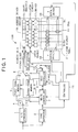
- a panel driving device 100 is provided with: an analog-to-digital (A/D) converter 1 that converts an analog video signal to input video image data; a sync separator 2 that separates a sync signal from the analog video signal and outputs the separated sync signal; first and second frame memories 3 and 4 each of which stores the video image data; a write switch 5 that selects one of the frame memories to which the video image data are to be written; a read switch 6 that selects one of the frame memories from which the video image data are to be read; a write controller 7 that controls the write switch 5; a read controller 8 that controls the read switch 6; a controller 11 that controls various parts of the device; an AND circuit 12 that computes the AND of a first clock pulse from the controller 11 with a signal HA from the read controller 8; and a delay section 13 that adjusts output timing of pulses from the AND circuit 12.
- A/D analog-to-digital
- the panel driving device 100 is further provided with: a shift register 15 that stores address data (pixel data) for each line; an address driver section 18 having a latch circuit 16 and a driver 17; a Y sustain driver 19 that applies Y sustain pulses to sustain electrodes Y1 to Yn simultaneously, and an X sustain driver 20 that applies X sustain pulses to sustain electrodes X1 to Xn simultaneously.
- the latch circuit 16 of the driver section 18 latches, after address data for each line have been loaded to the shift register 15, the address data for the line, and the driver 17 of the driver section 18 generates data pulses corresponding to the latched address data and applies the generated data pulses to column electrodes D1 to Dm simultaneously.
- the panel driving device 100 drives a plasma display panel 21 on a field interval basis.
- a single field interval consists of a plurality of subfields SF1 to SFN.
- each subfield includes an address phase for selecting cells 22 to be illuminated, and a sustain phase for continuously illuminating the selected cells 22. Additionally, a reset phase precedes the first subfield SF1 to completely stop the illumination of the previous field.
- the durations of the sustain phases of the respective subfields are gradually increased in order of the subfields SF1 to SFN, for gray scale display.
- address scanning is performed one line at a time. That is, a scan pulse is applied to the electrode Y1 constituting a first line, and simultaneously therewith, data pulses DP1 corresponding to the address data for cells belonging to the first line are applied to the column electrodes D1 to Dm. Then, a scan pulse is applied to the electrode Y2 constituting a second line, and simultaneously therewith, data pulses DP2 corresponding to the address data for cells belonging to the second line are applied to the column electrodes D1 to Dm.
- Scan and data pulses are similarly applied to the third and subsequent lines, and finally, a scan pulse is applied to the electrode Yn constituting an nth line, and simultaneously therewith, data pulses DPn corresponding to the address data for cells belonging to the nth line are applied to the column electrodes D1 to Dm.
- X sustain pulses and Y sustain pulses are repetitively applied to the electrodes X1 to Xn and electrodes Y1 to Yn at predetermined timings, respectively.
- the address data from the A/D converter 1 are written, field by field, alternately to the first frame memory 3 and the second frame memory 4 as selected by the write switch 5.
- the input video image data in the first and second frame memories 3 and 4 are read alternately from the first and second frame memories 3 and 4 as selected by the read switch 6 one field behind that of their write timing.
- the address data read from the first or second frame memory 3 or 4 are sequentially loaded to the shift register one line at a time according to respective second clock (shift clock) pulses.
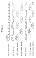
- a latch enable signal to be input to the latch circuit 16 rises upon rise of a second clock pulse for loading the last data item z for each line, and thus the address data for the line (e.g., data items a to z) are latched and then supplied to the driver 17 simultaneously.
- a scan pulse is applied to the corresponding one of the electrodes Y1 to Yn as mentioned above, and at the same time, data pulses DP1 to DPn corresponding to the read line-based address data are applied to the corresponding column electrodes D1 to Dm.
- the signal HA is output from the read controller 8 while the address data are read one line at a time from the first or second frame memory 3 or 4.
- both the signal HA and each first clock pulse from the controller 11 are fed to the AND circuit 12 to trigger passage of the first clock pulse so that each of second clock pulses is output only while the signal HA is being output (the level of the signal HA is high). That is, while the address data are not read from the first or second frame memory 3 or 4, no second clock pulses are output.
- Each second clock pulse passes through the delay section 13 to have its timing adjusted before output to the shift register 15.
- the panel driving device of the invention supply of shift clock pulses to the shift register is interrupted after each regular latch timing for reading predetermined address data.
- the device keeps latching correct address data.
- the display panel provides a display which is in accord with the correct address data on its screen, with no noise marks present in the picture displayed on its screen.
Landscapes
- Engineering & Computer Science (AREA)
- Physics & Mathematics (AREA)
- Power Engineering (AREA)
- Plasma & Fusion (AREA)
- Computer Hardware Design (AREA)
- General Physics & Mathematics (AREA)
- Theoretical Computer Science (AREA)
- Control Of Indicators Other Than Cathode Ray Tubes (AREA)
- Control Of Gas Discharge Display Tubes (AREA)
- Liquid Crystal Display Device Control (AREA)
- Control Of El Displays (AREA)
Abstract
Description
Claims (7)
- A panel driving device characterized by:a shift register (15) for sequentially storing address data according to shift clock pulses;a latch circuit (16) for latching the address data stored in the shift register;a drive circuit (17) for driving a display panel (21) based on the address data output from the latch circuit; anda clock interrupting device (12) for interrupting supply of the shift clock pulses to the shift register after a regular timing for causing the latch circuit to latch predetermined address data stored in the shift register.
- The panel driving device according to claim 1, wherein the device further comprises:wherein the clock interrupting device (12) includes a detecting device (12) for detecting an event in which the predetermined address data are not being read by the reading device, and interrupts supply of the shift clock pulses to the shift register while the detecting device detects the event in which the predetermined address data are not being read.a storage device (3, 4) for storing the address data to be supplied to the shift register; anda reading device (8) for reading the address data stored in the storage device to load the read address data to the shift register,
- The panel driving device according to claim 2, wherein the reading device (8) outputs a predetermined signal indicative of the event in which the predetermined address data are not being read, and the detecting device detects the event in which the predetermined address data are not being read, based on the predetermined signal.
- The panel drive device according to claim 2 or 3, wherein the clock interrupting device (12) includes a gate device (12) for selectively triggering passage of another group of clock pulses supplied to the clock interrupting device, as the shift clock pulses, so that the gate device selects passage or nonpassage of the shift clock pulses depending on a result of detection performed by the detecting device (12).
- The panel driving device according to claim 4, wherein the clock interrupting device (12) includes a delay device (13) for adjusting output timing of the shift clock pulses from the gate device.
- The panel driving device according to any one of claims 1 to 5, wherein the display panel is a plasma display panel (21).
- The panel driving device according to claim 6, further comprising a light emission maintenance device for applying sustain pulses to the plasma display panel to cause selected pixels to continuously emit light, the pixels being selected based on the address data.
Applications Claiming Priority (2)
| Application Number | Priority Date | Filing Date | Title |
|---|---|---|---|
| JP2001190331A JP2003005703A (en) | 2001-06-22 | 2001-06-22 | Panel driving device |
| JP2001190331 | 2001-06-22 |
Publications (4)
| Publication Number | Publication Date |
|---|---|
| EP1288898A2 true EP1288898A2 (en) | 2003-03-05 |
| EP1288898A3 EP1288898A3 (en) | 2003-09-03 |
| EP1288898B1 EP1288898B1 (en) | 2007-08-15 |
| EP1288898B9 EP1288898B9 (en) | 2008-03-05 |
Family
ID=19029117
Family Applications (1)
| Application Number | Title | Priority Date | Filing Date |
|---|---|---|---|
| EP02254444A Expired - Lifetime EP1288898B9 (en) | 2001-06-22 | 2002-06-24 | Panel driving device |
Country Status (4)
| Country | Link |
|---|---|
| US (1) | US6914591B2 (en) |
| EP (1) | EP1288898B9 (en) |
| JP (1) | JP2003005703A (en) |
| DE (1) | DE60221759T2 (en) |
Families Citing this family (10)
| Publication number | Priority date | Publication date | Assignee | Title |
|---|---|---|---|---|
| JP2004252017A (en) * | 2003-02-19 | 2004-09-09 | Pioneer Electronic Corp | Display panel driving device |
| EP1667095B1 (en) | 2003-08-07 | 2009-10-14 | Panasonic Corporation | Display device |
| JP2005208413A (en) * | 2004-01-23 | 2005-08-04 | Ricoh Co Ltd | Image processing apparatus and image display apparatus |
| US7046227B2 (en) * | 2004-08-17 | 2006-05-16 | Seiko Epson Corporation | System and method for continuously tracing transfer rectangles for image data transfers |
| CA2586574A1 (en) * | 2004-11-30 | 2007-06-08 | Telefonaktiebolaget Lm Ericsson (Publ) | Method for smm capability distribution |
| JP2007310245A (en) * | 2006-05-19 | 2007-11-29 | Eastman Kodak Co | Driver circuit |
| KR20090081627A (en) * | 2008-01-24 | 2009-07-29 | 삼성에스디아이 주식회사 | Plasma display device, driving method thereof and driving device |
| JP5346520B2 (en) | 2008-08-13 | 2013-11-20 | 株式会社ジャパンディスプレイ | Image display device |
| JP2010145709A (en) * | 2008-12-18 | 2010-07-01 | Hitachi Displays Ltd | Image display device |
| KR101807246B1 (en) * | 2011-01-11 | 2017-12-11 | 삼성디스플레이 주식회사 | Display device |
Family Cites Families (12)
| Publication number | Priority date | Publication date | Assignee | Title |
|---|---|---|---|---|
| US3942149A (en) * | 1974-08-19 | 1976-03-02 | Texas Instruments Incorporated | Solid state depth sounder |
| JPS5771063A (en) * | 1980-10-22 | 1982-05-01 | Toshiba Corp | Conversion and storage system for picture information |
| US4844590A (en) * | 1985-05-25 | 1989-07-04 | Canon Kabushiki Kaisha | Method and apparatus for driving ferroelectric liquid crystal device |
| US5227790A (en) * | 1991-01-31 | 1993-07-13 | Oki Electric Industry Co., Ltd. | Cascaded drive units having low power consumption |
| JP3582082B2 (en) * | 1992-07-07 | 2004-10-27 | セイコーエプソン株式会社 | Matrix display device, matrix display control device, and matrix display drive device |
| JP2822911B2 (en) * | 1995-03-23 | 1998-11-11 | 日本電気株式会社 | Drive circuit |
| JP3593448B2 (en) * | 1997-02-07 | 2004-11-24 | 株式会社 日立ディスプレイズ | Liquid crystal display device and data signal line driver |
| TW373115B (en) * | 1997-02-07 | 1999-11-01 | Hitachi Ltd | Liquid crystal display device |
| KR100217279B1 (en) * | 1997-06-20 | 1999-09-01 | 전주범 | Main clock separation application method for gray scale processing of PDP-TV system. |
| JP4163787B2 (en) * | 1997-06-20 | 2008-10-08 | 株式会社大宇エレクトロニクス | Apparatus and method for timing control of AC plasma display flat plate apparatus |
| US6492973B1 (en) * | 1998-09-28 | 2002-12-10 | Sharp Kabushiki Kaisha | Method of driving a flat display capable of wireless connection and device for driving the same |
| JP2001159877A (en) | 1999-09-20 | 2001-06-12 | Sharp Corp | Matrix type image display device |
-
2001
- 2001-06-22 JP JP2001190331A patent/JP2003005703A/en active Pending
-
2002
- 2002-06-21 US US10/176,406 patent/US6914591B2/en not_active Expired - Fee Related
- 2002-06-24 DE DE60221759T patent/DE60221759T2/en not_active Expired - Fee Related
- 2002-06-24 EP EP02254444A patent/EP1288898B9/en not_active Expired - Lifetime
Also Published As
| Publication number | Publication date |
|---|---|
| DE60221759D1 (en) | 2007-09-27 |
| EP1288898B9 (en) | 2008-03-05 |
| EP1288898A3 (en) | 2003-09-03 |
| US6914591B2 (en) | 2005-07-05 |
| DE60221759T2 (en) | 2008-05-15 |
| US20020196225A1 (en) | 2002-12-26 |
| EP1288898B1 (en) | 2007-08-15 |
| JP2003005703A (en) | 2003-01-08 |
Similar Documents
| Publication | Publication Date | Title |
|---|---|---|
| US20010005202A1 (en) | Plasma display with improved reactivation characteristic, driving method for plasma display, wave generating circuit with reduced memory capacity, and planar matrix type display using wave generating circuit | |
| CN100487765C (en) | Display control device of display panel | |
| JP4010983B2 (en) | Plasma display panel address data automatic power control method and apparatus, and plasma display panel apparatus having the apparatus | |
| US6914591B2 (en) | Panel driving device | |
| US6967646B2 (en) | Display controller and display apparatus | |
| US6473061B1 (en) | Plasma display panel drive method and apparatus | |
| JPH10207427A (en) | Driving method for plasma display panel display device and driving control device | |
| KR100929749B1 (en) | Video display device, driver for video display device and video display method | |
| US20050057448A1 (en) | Method for controlling address power on plasma display panel and apparatus thereof | |
| KR20000003326A (en) | Control apparatus of sustain purse for pdp | |
| US8125410B2 (en) | Plasma display having latch failure detecting function | |
| KR100922353B1 (en) | Plasma display device and driving method thereof | |
| JP2000261739A (en) | Driving device for plasma display | |
| EP1463024B1 (en) | Apparatus and method for driving plasma display panel | |
| JP2002140031A (en) | Display device driving device and display device | |
| JP3382451B2 (en) | Information input device and display device | |
| KR20060103231A (en) | Driving Method of Plasma Display Panel and Plasma Display Device | |
| JPH10274957A (en) | Drive circuit for plasma display | |
| KR100237204B1 (en) | Plasma display device for computer monitor and its driving method | |
| KR100257484B1 (en) | Plasma display panel and its control method | |
| KR100522799B1 (en) | Diagnosis apparatus for plasma display panel | |
| JPS62206589A (en) | Display unit driving system | |
| KR100489277B1 (en) | Method and apparatus for driving plasma display panel | |
| JPH10274954A (en) | Drive circuit for plasma display panel | |
| KR100531096B1 (en) | Device for driving plasma display panel and method thereof |
Legal Events
| Date | Code | Title | Description |
|---|---|---|---|
| PUAI | Public reference made under article 153(3) epc to a published international application that has entered the european phase |
Free format text: ORIGINAL CODE: 0009012 |
|
| AK | Designated contracting states |
Kind code of ref document: A2 Designated state(s): AT BE CH CY DE DK ES FI FR GB GR IE IT LI LU MC NL PT SE TR Designated state(s): AT BE CH CY DE DK ES FI FR GB GR IE IT LI LU MC NL PT SE TR |
|
| AX | Request for extension of the european patent |
Extension state: AL LT LV MK RO SI |
|
| PUAL | Search report despatched |
Free format text: ORIGINAL CODE: 0009013 |
|
| RAP1 | Party data changed (applicant data changed or rights of an application transferred) |
Owner name: PIONEER DISPLAY PRODUCTS CORPORATION Owner name: PIONEER CORPORATION |
|
| AK | Designated contracting states |
Kind code of ref document: A3 Designated state(s): AT BE CH CY DE DK ES FI FR GB GR IE IT LI LU MC NL PT SE TR |
|
| AX | Request for extension of the european patent |
Extension state: AL LT LV MK RO SI |
|
| 17P | Request for examination filed |
Effective date: 20030915 |
|
| AKX | Designation fees paid |
Designated state(s): DE FR GB |
|
| 17Q | First examination report despatched |
Effective date: 20040806 |
|
| GRAP | Despatch of communication of intention to grant a patent |
Free format text: ORIGINAL CODE: EPIDOSNIGR1 |
|
| GRAS | Grant fee paid |
Free format text: ORIGINAL CODE: EPIDOSNIGR3 |
|
| GRAA | (expected) grant |
Free format text: ORIGINAL CODE: 0009210 |
|
| AK | Designated contracting states |
Kind code of ref document: B1 Designated state(s): DE FR GB |
|
| REG | Reference to a national code |
Ref country code: GB Ref legal event code: FG4D |
|
| REF | Corresponds to: |
Ref document number: 60221759 Country of ref document: DE Date of ref document: 20070927 Kind code of ref document: P |
|
| ET | Fr: translation filed | ||
| PLBE | No opposition filed within time limit |
Free format text: ORIGINAL CODE: 0009261 |
|
| STAA | Information on the status of an ep patent application or granted ep patent |
Free format text: STATUS: NO OPPOSITION FILED WITHIN TIME LIMIT |
|
| 26N | No opposition filed |
Effective date: 20080516 |
|
| GBPC | Gb: european patent ceased through non-payment of renewal fee |
Effective date: 20080624 |
|
| REG | Reference to a national code |
Ref country code: FR Ref legal event code: ST Effective date: 20090228 |
|
| PG25 | Lapsed in a contracting state [announced via postgrant information from national office to epo] |
Ref country code: DE Free format text: LAPSE BECAUSE OF NON-PAYMENT OF DUE FEES Effective date: 20090101 |
|
| PG25 | Lapsed in a contracting state [announced via postgrant information from national office to epo] |
Ref country code: GB Free format text: LAPSE BECAUSE OF NON-PAYMENT OF DUE FEES Effective date: 20080624 |
|
| PG25 | Lapsed in a contracting state [announced via postgrant information from national office to epo] |
Ref country code: FR Free format text: LAPSE BECAUSE OF NON-PAYMENT OF DUE FEES Effective date: 20080630 |