EP1288668A2 - System and method for testing electronic device interconnections - Google Patents
System and method for testing electronic device interconnections Download PDFInfo
- Publication number
- EP1288668A2 EP1288668A2 EP02255349A EP02255349A EP1288668A2 EP 1288668 A2 EP1288668 A2 EP 1288668A2 EP 02255349 A EP02255349 A EP 02255349A EP 02255349 A EP02255349 A EP 02255349A EP 1288668 A2 EP1288668 A2 EP 1288668A2
- Authority
- EP
- European Patent Office
- Prior art keywords
- pressure
- interconnections
- electronic device
- sensitive film
- interconnection
- Prior art date
- Legal status (The legal status is an assumption and is not a legal conclusion. Google has not performed a legal analysis and makes no representation as to the accuracy of the status listed.)
- Withdrawn
Links
Images


Classifications
-
- G—PHYSICS
- G01—MEASURING; TESTING
- G01R—MEASURING ELECTRIC VARIABLES; MEASURING MAGNETIC VARIABLES
- G01R31/00—Arrangements for testing electric properties; Arrangements for locating electric faults; Arrangements for electrical testing characterised by what is being tested not provided for elsewhere
- G01R31/50—Testing of electric apparatus, lines, cables or components for short-circuits, continuity, leakage current or incorrect line connections
- G01R31/66—Testing of connections, e.g. of plugs or non-disconnectable joints
- G01R31/70—Testing of connections between components and printed circuit boards
Definitions
- PGAs pin grid arrays
- BGAs ball grid arrays
- CSPs chip scale packages
- standard leaded components regularly employ well over one hundred interconnections, each of which is critical to the proper performance of the device.
- probes for testing printed circuit boards, electronic components such as integrated circuits (ICs), and IC wafers must also be tested for quality prior to being employed in the test environment. Such probes may number in the thousands, further exacerbating the problems of testing such interconnections. As manual visual inspection of such interconnections and probes is necessarily slow and error-prone, automated systems have been devised to perform such inspection.
- structured light may be used to illuminate a single interconnection or a row of interconnections at an oblique angle, creating shadows of the interconnections.
- an expected shadow size and shape can be determined and compared to the actual shadow cast by the interconnection to determine the quality of the interconnection.
- laser light can be projected substantially from the side of the connections so that opposing light detectors, by virtue of the laser light received, may be employed to determine if any interconnections are missing or are too short to be effective.
- such systems generally require rather complex and expensive optics.
- Embodiments of the invention provide a system and method for testing the quality of electronic device interconnections by way of a pressure-sensitive medium, such as, for example, a pressure-sensitive film.
- a pressure-sensitive medium such as, for example, a pressure-sensitive film.
- the interconnections of an electronic device are placed in contact with the pressure-sensitive medium, possibly by way of a robotic actuator.
- a mechanical force is then applied to the electronic device so that each interconnection of the electronic device exerts substantially identical pressure on the pressure-sensing medium, assuming no defects in the interconnections exist.
- the pressure-sensitive means produces an indication of the pressure exerted by each interconnection. That indication is then analyzed, possibly by way of a camera and associated computer, to determine the quality of the interconnections.
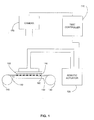
- FIG. 1 A system of testing the quality of interconnections of an electronic device according to an embodiment of the invention is shown in FIG. 1.
- An electronic device 100 has a plurality of interconnections 105 that extend from the main body of electronic device 100.
- electronic device 100 is a ball grid array (BGA) package holding an integrated circuit (IC) (not visible).
- BGA ball grid array
- IC integrated circuit
- CSPs chip-scale packages
- PGA pin grid array
- interconnections for larger electronic devices such as bed-of-nails testers for printed circuit boards, ICs, various electronic components, and IC wafers, may also be tested using such a system.
- electronic device 100 is placed so that interconnections 105 make contact with a pressure-sensitive film 130. Furthermore, the embodiment utilizes a substantially flat surface 150 against which film 130 is pressed by interconnections 105.
- Film 130 versions of which are manufactured by companies such as Fuji Photo Film and Sensor Products, Inc., displays a predetermined color in areas where pressure has been applied, thus displaying a visual image on the film representing areas on which a particular amount of pressure on the film has been exceeded.
- the color generated is initially contained in microcapsules within the film that burst when an imposed external pressure is exceeded. The visual image, as will be shown later, thus provides an indication of the quality of interconnections 105.
- At least three different types of pressure-sensitive film 130 are contemplated by the invention.
- a binary type of film all of the microcapsules burst at the same pressure level, thus indicating the areas where the pressure imposed met or exceeded a particular predetermined pressure level.
- a gray-scale type of film integrates microcapsules that burst at varying pressure levels.
- the color density in a particular area is associated with the amount of pressure applied to that area.
- Gray-scale films are the most common type currently being manufactured in the pressure-sensitive film industry.
- embodiments of the present invention contemplate the use of color pressure-sensitive film, whereby different pressures are indicated by varying colors on the film, providing comparable pressure resolution to gray-scale films, resulting in more accurate test results than binary films.
- a mechanical force is applied to electronic device 100 by a robotic actuator 120, which is normally controlled by a test controller 110.
- Test controller 110 may be any algorithmic controller, such as a general-purpose computer or a microcontroller-based embedded controller.
- Robotic actuator 120 is capable of accurately applying a predetermined amount of force to electronic device 100 that is appropriate for electronic device 100 and the type of film 130 involved. Such force is applied evenly to electronic device 100 so that all interconnections 105 exert substantially identical pressure on film 130, assuming that all interconnections 105 are of acceptable quality.
- robotic actuator 120 could be capable of placing electronic device 100 in contact with film 130 prior to the testing of device 100, as well as removing device 100 from film 130 after the test has been completed. Alternately, electronic device 100 may be placed onto and removed from film 130 manually, or a separate robotic actuator (not shown) may be used for that purpose.
- film 130 Due to the permanent nature of the visual image on pressure-sensitive film 130 after pressure has been applied, a new portion of film 130 is required for each electronic device 100 tested. Replacement of film 130 for each new device may be performed manually. To automate the film replacement process, film 130 could be fashioned as a long strip loaded onto a pair of motor-driven spools 140, as shown in FIG. 1. Such a mechanism would allow film 130 to be advanced a sufficient amount so that a previously unused portion of film 130 would be available for each electronic device 100 to be tested.
- Camera 170 in some embodiments, is a typical area array camera. Alternately, camera 170 could be a line scan camera, which typically results in the generation of a higher-resolution electronically recorded image. Such additional resolution may be required or desired, depending on the type of electronic device 100 being tested and the type of film 130 being employed.
- a second embodiment of the invention allows camera 170 to generate the electronically recorded image while electronic device 100 is still in contact with film 130.
- camera 170 is situated on the opposing side of film 130 from electronic device 100.
- a transparent platen 200 is utilized as a more specific type of flat surface 150 (from FIG. 1) so that camera 170 may have direct line of sight to film 130 prior to the removal of electronic device 100 from film 130.
- a benefit of this embodiment is that several electronically recorded images of the visual image on film 130 may be generated at increasing levels of force applied on electronic device 100. The additional information gathered from multiple electronically recorded images at different applied pressures could further aid in determining the quality of interconnections 105.
- FIG. 3 displays an example binary visual image 300 on film 130 produced by interconnections 105 of electronic device 100, which, in this case, is a 256-interconnection BGA. Since film 130 is binary in this particular case, no gray levels are depicted. Therefore, the quality of interconnections 105 is determined by the presence, location, and size of the dark areas of image 300. For example, a missing spot 310, in a location where a BGA solder ball would be expected, indicates a poor or nonexistent interconnection. Other problems, such as coplanarity, may also be detected. For instance, a warped BGA package, which is one example of a coplanarity problem, may result in small spots 320 being smaller when compared to others generated by interconnection 105 of the BGA package. Such small spots 320 would thus indicate that less pressure is being applied by the associated interconnection at that comer of the package, possibly resulting in poor connectivity when the package is installed in the electronic system for which it was intended.
- a warped BGA package which is one example of a co
- a related visual image 400 is shown in FIG. 4 using the same BGA package.
- Image 400 is either gray-scale or color in nature, derived from either a gray-scale or color pressure-sensitive film.
- each spot of a high quality interconnection would be indicated by a set of concentric rings of a single color with varying intensity, or concentric rings of varying color, thus indicating the spherical nature of the solder balls.
- a missing or short ball would still be indicated by a missing spot 410, as was the case with binary image 300.
- the coplanarity problem of the BGA package would also be detected in image 400, with smaller, lighter spots 420 indicating that those solder balls were not residing in the same plane as the majority of those attached to the package.
- a light spot 430 may be seen, indicating that the associated solder ball is probably flatter than others on the package, therefore possibly causing an interconnection problem.
- gray-scale or color pressure-sensitive film would also enhance the testing of spring-loaded interconnection pins of bed-of-nails testers commonly used for PCBs, ICs, and IC wafers.
- the pressure of such pins is normally critical to the ability of the tester to accurately detect errors in the devices under test, as pins that exert too little pressure may not make proper contact with the device, while those that exert too much pressure may prevent surrounding pins from making proper contact with the device.
- an indication of how much spring pressure is associated with each interconnection pin aids in detecting testability problems before the bed-of-nails tester is placed into service.
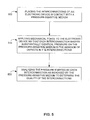
- the present invention is also embodied as a method of testing the quality of electronic device interconnections by way of mechanical pressure measurements.
- a pressure-sensitive medium such as, for example, pressure-sensitive film
- a mechanical force is then applied to the electronic device so that each interconnection exerts substantially identical pressure on the pressure-sensitive medium, assuming that no defects exist in the interconnections (step 510).
- an indication of the pressure exerted by each of the interconnections is produced on the pressure-sensitive medium.
- the indication of the pressures on the medium is analyzed to determine the quality of each of the connections on the electronic device (step 520).
- the embodiments of the invention have been shown to provide an effective electronic device interconnection quality testing system and method that utilizes mechanical pressure to discover defects in the device interconnections. As each interconnection of an electronic device is tested simultaneously, testing time is limited. Also, since special lighting is not required, the expense of special optics, and the difficulties inherent in using structured light for testing such interconnections, is eliminated. Other specific systems and methods embodying the invention are also possible. Therefore, the present invention is not to be limited to the specific forms so described and illustrated; the invention is limited only by the claims.
Landscapes
- Physics & Mathematics (AREA)
- General Physics & Mathematics (AREA)
- Testing Of Individual Semiconductor Devices (AREA)
- Force Measurement Appropriate To Specific Purposes (AREA)
- Testing Or Measuring Of Semiconductors Or The Like (AREA)
Abstract
Description
Claims (10)
- A system for testing the quality of interconnections of electronic devices, comprising:means for sensing mechanical pressure;means for placing the interconnections (105) of an electronic device (100) in contact with the pressure-sensing means;means for applying a mechanical force to the electronic device (100) so that each interconnection (105) of the electronic device (100) exerts substantially identical pressure on the pressure-sensing means in the absence of defects in the interconnections (105), the pressure-sensing means producing an indication of the pressure exerted by each interconnection (105); andmeans for analyzing the pressure exerted by each interconnection (105) of the electronic device (100) as indicated by the pressure-sensing means to determine the quality of the interconnections (105).
- A system as claimed in claim 1, wherein:said means for sensing comprises a pressure-sensitive film (130);said means for placing comprises a flat surface (150);said means for applying comprises a robotic actuator (120) that places the interconnections (105) of an electronic device (100) in contact with the pressure-sensitive film (130), the robotic actuator (120) also applying a mechanical force to the electronic device (100) so that each interconnection (105) of the electronic device (100) exerts substantially identical pressure on the pressure-sensitive film (130) in the absence of defects in the interconnections (105), the pressure-sensitive film (130) being pressed between the interconnections (105) and the flat surface (150), the pressure-sensitive film (130) producing an indication of the pressure exerted by each interconnection (105) by way of a visual image (160) on the film;
and said means for analysing comprises a camera (170) that generates an electronically recorded image based on the visual image (160) indicated on the pressure-sensitive film (130); and
a test controller (110) that interprets the electronically recorded image from the camera (170) to determine the quality of the interconnections (105). - A system as claimed in claim 2, wherein the pressure-sensitive film (130) is a binary pressure-sensitive film.
- A system as claimed in claim 2, wherein the pressure-sensitive film (130) is a gray-scale pressure-sensitive film that indicates different contact pressures by different intensities of a single color.
- A system as claimed in claim 2, wherein the pressure-sensitive film (130) is a color pressure-sensitive film that indicates different contact pressures by different colors.
- A system as claimed in any of claims 2 to 5, further comprising a pair of motor-driven spools (140) upon which a roll of the pressure-sensitive film (130) resides so that subsequent electronic devices (100) may be tested using a previously unused portion of the pressure-sensitive film (130) by advancing the motor-driven spools (140).
- A system as claimed in any of claims 2 to 6, wherein the camera (170) is an area array camera.
- A system as claimed in any of claims 2 to 6, wherein the camera (170) is a line scan camera.
- A system as claimed in any of claims 2 to 8, wherein the robotic actuator (120) is capable of applying several different magnitudes of force on the electronic device (100) so that the quality of the interconnections (105) of the electronic device (100) may be analyzed at multiple magnitudes of force by the test controller (110).
- A method for testing the quality of interconnections of electronic devices, comprising the steps of:placing (500) the interconnections of an electronic device in contact with a pressure-sensitive medium;applying (510) a mechanical force to the electronic device so that each interconnection of the electronic device exerts substantially identical pressure on the pressure-sensitive medium in the absence of defects in the interconnections, the pressure-sensitive medium producing an indication of the pressure exerted by each interconnection; andanalyzing (520) the pressure exerted by each interconnection of the electronic device as indicated by the pressure-sensitive medium to determine the quality of the interconnections.
Applications Claiming Priority (2)
| Application Number | Priority Date | Filing Date | Title |
|---|---|---|---|
| US09/919,256 US6512387B1 (en) | 2001-07-31 | 2001-07-31 | Pressure-sensitive system and method of testing electronic device interconnections |
| US919256 | 2001-07-31 |
Publications (2)
| Publication Number | Publication Date |
|---|---|
| EP1288668A2 true EP1288668A2 (en) | 2003-03-05 |
| EP1288668A3 EP1288668A3 (en) | 2003-12-17 |
Family
ID=25441784
Family Applications (1)
| Application Number | Title | Priority Date | Filing Date |
|---|---|---|---|
| EP02255349A Withdrawn EP1288668A3 (en) | 2001-07-31 | 2002-07-31 | System and method for testing electronic device interconnections |
Country Status (4)
| Country | Link |
|---|---|
| US (1) | US6512387B1 (en) |
| EP (1) | EP1288668A3 (en) |
| SG (1) | SG114526A1 (en) |
| TW (1) | TWI225156B (en) |
Families Citing this family (18)
| Publication number | Priority date | Publication date | Assignee | Title |
|---|---|---|---|---|
| US7190440B2 (en) * | 2002-09-17 | 2007-03-13 | Seagate Technology, Llc | Controlling compressive force using pressure sensitive film |
| TWI221531B (en) * | 2002-10-25 | 2004-10-01 | Hwan-Chia Chang | Method for testing soldering reliability |
| TWI339737B (en) | 2005-04-27 | 2011-04-01 | Aehr Test Systems | Contactor assembly, cartridge, and apparatus and method for testing integrated circuit of device |
| US20080124528A1 (en) * | 2006-11-29 | 2008-05-29 | Motorola, Inc. | Printed electronic device and methods of determining the electrical value thereof |
| US7800382B2 (en) | 2007-12-19 | 2010-09-21 | AEHR Test Ststems | System for testing an integrated circuit of a device and its method of use |
| US8030957B2 (en) | 2009-03-25 | 2011-10-04 | Aehr Test Systems | System for testing an integrated circuit of a device and its method of use |
| US9703623B2 (en) * | 2014-11-11 | 2017-07-11 | Lenovo Enterprise Solutions (Singapore) Pte. Ltd. | Adjusting the use of a chip/socket having a damaged pin |
| KR102842851B1 (en) | 2016-01-08 | 2025-08-05 | 에어 테스트 시스템즈 | Method and system for thermal control of devices in an electronics tester |
| JP2017129395A (en) * | 2016-01-19 | 2017-07-27 | 三菱電機株式会社 | Semiconductor device inspection apparatus and semiconductor device inspection method |
| WO2018013727A1 (en) | 2016-07-12 | 2018-01-18 | Deka Products Limited Partnership | System and method for applying force to a device |
| US11299705B2 (en) | 2016-11-07 | 2022-04-12 | Deka Products Limited Partnership | System and method for creating tissue |
| KR20250126857A (en) * | 2017-03-03 | 2025-08-25 | 에어 테스트 시스템즈 | Cartridge, test piece and method of testing one or more electronic devices |
| US11126195B2 (en) * | 2017-06-12 | 2021-09-21 | Faraday & Future Inc. | System and method for detecting occluded objects based on image processing |
| JP7667260B2 (en) | 2020-10-07 | 2025-04-22 | エイアー テスト システムズ | Electronic Test Equipment |
| CN112964399B (en) * | 2021-04-05 | 2022-07-29 | 西北工业大学 | Full-automatic tester and testing method for contact pressure of metal wire/spring piece of electronic device |
| US12326376B1 (en) * | 2022-12-21 | 2025-06-10 | Hrl Laboratories, Llc | Spike arrays for small displacement force measurement |
| CN121114724A (en) | 2022-12-30 | 2025-12-12 | 雅赫测试系统公司 | Electronic tester |
| TW202524092A (en) * | 2023-11-30 | 2025-06-16 | 聯華電子股份有限公司 | Automatic calibration method and automatic calibration equipment for testing probe set used in semiconductor process |
Family Cites Families (3)
| Publication number | Priority date | Publication date | Assignee | Title |
|---|---|---|---|---|
| GB2263980B (en) * | 1992-02-07 | 1996-04-10 | Marconi Gec Ltd | Apparatus and method for testing bare dies |
| JP3787185B2 (en) * | 1995-04-28 | 2006-06-21 | アヴェンティス・リサーチ・ウント・テクノロジーズ・ゲーエムベーハー・ウント・コー・カーゲー | Device for detecting wiring defects on wiring boards |
| US5894161A (en) * | 1997-02-24 | 1999-04-13 | Micron Technology, Inc. | Interconnect with pressure sensing mechanism for testing semiconductor wafers |
-
2001
- 2001-07-31 US US09/919,256 patent/US6512387B1/en not_active Expired - Fee Related
-
2002
- 2002-01-30 SG SG200200586A patent/SG114526A1/en unknown
- 2002-01-31 TW TW091101680A patent/TWI225156B/en active
- 2002-07-31 EP EP02255349A patent/EP1288668A3/en not_active Withdrawn
Also Published As
| Publication number | Publication date |
|---|---|
| EP1288668A3 (en) | 2003-12-17 |
| SG114526A1 (en) | 2005-09-28 |
| US20030025494A1 (en) | 2003-02-06 |
| TWI225156B (en) | 2004-12-11 |
| US6512387B1 (en) | 2003-01-28 |
Similar Documents
| Publication | Publication Date | Title |
|---|---|---|
| US6512387B1 (en) | Pressure-sensitive system and method of testing electronic device interconnections | |
| US5862973A (en) | Method for inspecting solder paste in printed circuit board manufacture | |
| EP0160781B1 (en) | Measuring and detecting printed circuit wiring defects | |
| US5828449A (en) | Ring illumination reflective elements on a generally planar surface | |
| US6201892B1 (en) | System and method for arithmetic operations for electronic package inspection | |
| WO2000010115A1 (en) | System and method for image subtraction for ball and bumped grid array inspection | |
| US20070164763A1 (en) | Method for detecting abnormality of probe card | |
| JP2002515123A (en) | Inspection methods | |
| US7062080B2 (en) | Method of inspecting curved surface and device for inspecting printed circuit board | |
| JPH04158238A (en) | Inspecting method of liquid crystal panel | |
| EP1314974B1 (en) | Method of inspecting curved surface and device for inspecting printed circuit board | |
| JP2010091361A (en) | Method and device for inspecting image | |
| US6950549B2 (en) | Visual inspection method and visual inspection apparatus | |
| KR102883473B1 (en) | Deep Learning Based Image Sensor Wafer Test System | |
| WO2007102834A2 (en) | Optically enhanced probe alignment | |
| JPH09203765A (en) | Visual combination type board inspection device | |
| JP2007103860A (en) | Method of detecting probe contact trace, and prober | |
| JPH0611321A (en) | Solder print inspection method | |
| US7747066B2 (en) | Z-axis optical detection of mechanical feature height | |
| JP2013539012A (en) | Method for measuring particles adhering to an object | |
| JP2839411B2 (en) | Inspection device for defective IC | |
| JP2005134204A (en) | Characteristic inspection device, characteristic inspection method, and characteristic inspection program | |
| JPH08122273A (en) | Semiconductor device inspection method | |
| KR100485261B1 (en) | Bga socket test system | |
| JP2000088524A (en) | Mounting parts confirmation device |
Legal Events
| Date | Code | Title | Description |
|---|---|---|---|
| PUAI | Public reference made under article 153(3) epc to a published international application that has entered the european phase |
Free format text: ORIGINAL CODE: 0009012 |
|
| AK | Designated contracting states |
Kind code of ref document: A2 Designated state(s): AT BE BG CH CY CZ DE DK EE ES FI FR GB GR IE IT LI LU MC NL PT SE SK TR Designated state(s): AT BE BG CH CY CZ DE DK EE ES FI FR GB GR IE IT LI LU MC NL PT SE SK TR |
|
| AX | Request for extension of the european patent |
Extension state: AL LT LV MK RO SI |
|
| PUAL | Search report despatched |
Free format text: ORIGINAL CODE: 0009013 |
|
| AK | Designated contracting states |
Kind code of ref document: A3 Designated state(s): AT BE BG CH CY CZ DE DK EE ES FI FR GB GR IE IT LI LU MC NL PT SE SK TR |
|
| AX | Request for extension of the european patent |
Extension state: AL LT LV MK RO SI |
|
| RIC1 | Information provided on ipc code assigned before grant |
Ipc: 7G 01R 31/316 B Ipc: 7G 01R 31/30 A |
|
| 17P | Request for examination filed |
Effective date: 20040524 |
|
| AKX | Designation fees paid |
Designated state(s): DE GB IE |
|
| RAP1 | Party data changed (applicant data changed or rights of an application transferred) |
Owner name: AGILENT TECHNOLOGIES, INC. |
|
| GRAP | Despatch of communication of intention to grant a patent |
Free format text: ORIGINAL CODE: EPIDOSNIGR1 |
|
| RIC1 | Information provided on ipc code assigned before grant |
Ipc: G01R 31/04 20060101AFI20070213BHEP |
|
| STAA | Information on the status of an ep patent application or granted ep patent |
Free format text: STATUS: THE APPLICATION IS DEEMED TO BE WITHDRAWN |
|
| 18D | Application deemed to be withdrawn |
Effective date: 20070712 |