EP1286190A1 - Optical connection component - Google Patents
Optical connection component Download PDFInfo
- Publication number
- EP1286190A1 EP1286190A1 EP01925945A EP01925945A EP1286190A1 EP 1286190 A1 EP1286190 A1 EP 1286190A1 EP 01925945 A EP01925945 A EP 01925945A EP 01925945 A EP01925945 A EP 01925945A EP 1286190 A1 EP1286190 A1 EP 1286190A1
- Authority
- EP
- European Patent Office
- Prior art keywords
- optical
- protective resin
- silicone
- resin layer
- interconnection apparatus
- Prior art date
- Legal status (The legal status is an assumption and is not a legal conclusion. Google has not performed a legal analysis and makes no representation as to the accuracy of the status listed.)
- Withdrawn
Links
Images


Classifications
-
- G—PHYSICS
- G02—OPTICS
- G02B—OPTICAL ELEMENTS, SYSTEMS OR APPARATUS
- G02B6/00—Light guides; Structural details of arrangements comprising light guides and other optical elements, e.g. couplings
-
- G—PHYSICS
- G02—OPTICS
- G02B—OPTICAL ELEMENTS, SYSTEMS OR APPARATUS
- G02B6/00—Light guides; Structural details of arrangements comprising light guides and other optical elements, e.g. couplings
- G02B6/24—Coupling light guides
- G02B6/36—Mechanical coupling means
- G02B6/3608—Fibre wiring boards, i.e. where fibres are embedded or attached in a pattern on or to a substrate, e.g. flexible sheets
-
- G—PHYSICS
- G02—OPTICS
- G02B—OPTICAL ELEMENTS, SYSTEMS OR APPARATUS
- G02B6/00—Light guides; Structural details of arrangements comprising light guides and other optical elements, e.g. couplings
- G02B6/24—Coupling light guides
- G02B6/42—Coupling light guides with opto-electronic elements
- G02B6/43—Arrangements comprising a plurality of opto-electronic elements and associated optical interconnections
-
- G—PHYSICS
- G02—OPTICS
- G02B—OPTICAL ELEMENTS, SYSTEMS OR APPARATUS
- G02B6/00—Light guides; Structural details of arrangements comprising light guides and other optical elements, e.g. couplings
- G02B6/24—Coupling light guides
- G02B6/36—Mechanical coupling means
- G02B6/38—Mechanical coupling means having fibre to fibre mating means
- G02B6/3807—Dismountable connectors, i.e. comprising plugs
- G02B6/3887—Anchoring optical cables to connector housings, e.g. strain relief features
- G02B6/38875—Protection from bending or twisting
-
- G—PHYSICS
- G02—OPTICS
- G02B—OPTICAL ELEMENTS, SYSTEMS OR APPARATUS
- G02B6/00—Light guides; Structural details of arrangements comprising light guides and other optical elements, e.g. couplings
- G02B6/24—Coupling light guides
- G02B6/42—Coupling light guides with opto-electronic elements
- G02B6/4201—Packages, e.g. shape, construction, internal or external details
- G02B6/4219—Mechanical fixtures for holding or positioning the elements relative to each other in the couplings; Alignment methods for the elements, e.g. measuring or observing methods especially used therefor
- G02B6/4236—Fixing or mounting methods of the aligned elements
- G02B6/4239—Adhesive bonding; Encapsulation with polymer material
Definitions
- This invention relates to optical interconnection apparatus (optical circuit board connectors) for mutually connecting optical component, parts and/or devices used in optical communications or optical information processing, such as optical elements, optical circuit packs and optical circuit devices.
- optical components, optical circuit packs and optical circuit devices are provided at terminals thereof with optical connectors to interconnect them together via optical fibers.
- optical fibers have to be arranged with slacks in this case, it is a current practice that, on an optical circuit pack or inside and/or on a back side of an optical circuit devices, intricately routed lines of the optical fibers extend overlapping one another in the form of a bird's nest and hence occupy a large space.
- the optical interconnection apparatus disclosed in JP 2,574,611 B is obtained in such a way that upon its fabrication, optical fibers are located by a pressure-sensitive adhesive on a substrate (base layer) or on fiber jackets, to form a routing pattern and the routing pattern is then covered with the same material as the material used for the substrate, whereby a protective layer is formed.
- This process is however accompanied by problems in that as optical fibers so located increase in number and the optical fibers increase more overlapped portions (cross-over routing) in the routing pattern so formed, the resulting routing layer of the optical fibers becomes thicker and, because the tacky surface with which the optical fibers are in contact becomes smaller at the overlapped portions of the optical fibers, the protective layer cannot be arranged evenly.
- the surface of the formed protective resin layer composed of a silicone based rubber-like or gel-like material is easily broken and damaged, there is a problem of surface scratches when the optical interconnection apparatus is installed in a very narrow space such as in a rack or a board.
- an object of the present invention is to provide an optical interconnection apparatus free from attaching, fixing or adhering when came into contact with each other or with another material, and easy to handle.
- Another object of the present invention is to provide an optical interconnection apparatus having high flexibility and being easy to handle which makes it possible to readily interconnect optical components such as optical elements, optical circuit packs, optical circuit devices, etc.
- a first aspect of the optical interconnection apparatus which has a substrate, comprises a substrate, a protective resin layer composed of a silicone based rubber-like or gel-like material on one side or both sides of said substrate, and plural optical fibers which are two-dimensionally routed on the substrate so as to form a routing pattern having at least a crossing part, a curved part or a fiber pitch changing part and provided at ends thereof with end portions adapted to permit optical interconnections, and said optical fibers being held in place by said protective resin layer, wherein a non-tacky surface layer having a kinetic friction coefficient of 3 or less is provided on the surface of said protective resin layer.
- it is possible to prepare an optical interconnection apparatus having plural substrates by laminating a protective resin layer formed on a substrate with another protective resin layer formed on another substrate via an adhesive layer.
- a second aspect of the optical interconnection apparatus which has no substrate, comprises at least two protective resin layers composed of a silicone based rubber-like or gel-like material and plural optical fibers which are two-dimensionally routed so as to form a routing pattern having at least a crossing part, a curved part or a fiber pitch changing part and provided at ends thereof with end portions adapted to permit optical interconnections, and said optical fibers being held in place by at least one of said protective resin layers, wherein a non-tacky surface layer having a kinetic friction coefficient of 3 or less is provided on the surface of each of said protective resin layers.
- each of said protective resin layers may be laminated via an adhesive layer, too.
- the non-tacky surface layer is preferred to be composed of a silicone based material.
- a protective resin layer can be prepared by arranging an edge-dam member along or in a vicinity of a peripheral edge of a substrate, a release film or another protective resin layer, filling the inside of the edge-dam member with a silicone rubber-like or gel-like material, and solidifying it.
- 1 is a substrate
- 2 and 2a each is a protective resin layer
- 3 and 3a each is an adhesive layer
- 4 is an optical fiber
- 5 is an end portion
- 6 is an optical component
- 7 is an edge-dams
- 8 and 8a each is a non-tacky surface layer.
- plural optical fibers 4 are routed on a substrate 1 which has a two-dimensional plane via an adhesive layer 3. These optical fibers 4 are held in place and protected by a protective resin layer 2 having flexibility composed of a silicone based rubber-like or gel-like material. A non-tacky surface layer 8 is provided on the protective resin layer 2. Opposite ends of the optical fibers 4 are formed into end portions 5 adapted to permit optical interconnections. Optical components 6, for example, optical connectors are interconnected to the end portions. The end portions 5 may be formed in a body with the optical components 6. 7 is an edge-dam which is arranged for forming the protective resin layer.
- a protective resin layer 2a is provided on the back of the substrate 1, and a non-tacky surface layer 8a is formed on the surface of the protective resin layer 2a.
- plural optical fibers 4 are routed on a protective resin layer 2a having flexibility via an adhesive layer 3, and they are covered with a protective resin layer 2 having flexibility. Further, non-tacky surface layers 8 and 8a are formed on these protective resin layers 2 and 2a, respectively.
- FIG.5 an optical interconnection apparatus having four protective resin layers and two optical fiber layers is shown, which is produced using two parts before forming the non-tacky surface layers 8 and 8a in production of the optical interconnection apparatus of FIG. 4, stacking these two parts so as to face the protective resin layers 2a and 2a via an adhesive layer 3a, and forming then non-tacky surface layers 8 and 8 on each of the protective resin layers 2 and 2, respectively.
- the substrate having a two-dimensional plane for supporting the routed optical fibers thereon is usable insofar as it is employed in general electronic parts or electrical parts, such as glass-epoxy resin composite substrates, polyester films, polyimide films, and gel-like, rubber-like or porous organic materials such as silicone or polyurethane, etc., which may be of any shape.
- the substrate is not required to have flexibility but is stiff depending on its application purpose, though it is preferred to have a certain degree of flexibility. It is accordingly possible to use a stiff polymer substrate, a ceramic substrate or the like.
- Optical fibers to be routed in the present invention can be suitably selected and used depending on the application purpose of the optical interconnection apparatus.
- silica- or plastic-made single-mode optical fibers,multiple-mode optical fibers or the like can be used preferably.
- Carbon-coated optical fibers can also be suitably used as the optical fibers.
- optical fibers in the present invention As a routing method for optical fibers in the present invention, it is most convenient to route them by providing an adhesive layer on a film substrate. Nonetheless, a suitable method may be selected for the routing of optical fibers depending on the application purpose. It is only necessary to route optical fibers such that they are provided at both ends thereof with end portions adapted to permit interconnections. For example, it is possible to route optical fibers by arranging projecting members, recessed members or the like on a film substrate or by providing outer surfaces of the optical fibers with adhesive layers.
- any adhesive can be used insofar as it has adhesiveness sufficient to retain the pattern of the optical fibers in response to tensions which may be produced when the routed optical fibers are bent.
- Usable examples can include various pressure-sensitive adhesives (adhesives), thermoplastic adhesives and thermosetting adhesives, such as urethane-base adhesives, acrylic adhesives, epoxy-adhesives, nylon-base adhesives, phenol-base adhesives, polyimide-base adhesives, vinyl adhesives, silicone-base adhesives, rubber-base adhesives, fluorinated epoxy adhesives and fluorinated acrylic adhesives. From the standpoint of easiness in routing optical fibers, pressure-sensitive adhesives and thermoplastic adhesives are used preferably.
- silicone based gel-like or rubber-like materials excellent in reliability, stress relaxation, heat resistance, cold resistance, moisture resistance, chemical resistance, electric insulation and flexibility, which have been practically used as sealing materials for semiconductor devices can be used as the resins for composing the protective resin layers having flexibility.
- the protective resin layers are produced using a silicone-based material which hardens to be in a gel-like or rubber-like state. More specifically, addition reaction type silicone gel, condensation reaction room temperature vulcanizing type silicone rubber, addition reaction type thermosetting silicone rubber, addition reaction room temperature vulcanizing type silicone rubber, UV curing type silicone rubber, etc. can be used.
- any material can be used insofar as it adheres to the silicone based rubber-like or gel-like material of the protective resin layer and forms a film which reduces tackiness, adhesion, sticking tendency of the silicone based rubber-like or gel-like material by drying or curing at room temperature or with heat.
- the non-tacky surface layer is preferred to be formed of a silicone-based material.
- the non-tacky surface layer may contain a filler.
- non-tacky surface layer does not contain a filler in the present invention
- silicone resin, fluorine contained resin, urethane resin, olefin resin, polystyrene resin, acrylic resin, etc. can be used for composing the non-tacky surface layer.
- resins may be suitably selected to use as a composite material.
- a curable silicone resin composition is the most suitably used.
- a silicone resin having reactive groups which cause a condensation reaction in the molecule can be used as the silicone resin in the curable silicone resin composition.
- the condensation reaction group include hydroxyl group (silanol group), alkoxy group such as methoxy group and ethoxy group, and oxime group, which attached to the silicon atom.
- silicone resin examples include those which are composed of at least a siloxane unit represented by the formula RSiO 3 / 2 and a siloxane unit represented by the formula R 2 SiO 2 / 2 and have the above-mentioned reactive groups attached to the silicon atom.
- each R which is the same or different each other, represents a C 1 -C 10 monovalent hydrocarbon group such as alkyl group, for example, methyl, ethyl, propyl, etc., alkenyl group, such as vinyl, allyl-butenyl, etc., aryl group such as phenyl, tolyl, etc., and halogenated alkyl group such as 3,3,3-trifluoropropyl, etc.
- silicone resins include methylsilicone resin, methylphenylsilicone resin, methylvinylsilicone resin, etc. Of these, methylphenylsilicone resin is the most suitable because of its excellent film strength of the non-tacky surface layer.
- the curable silicone resin composition may contain a cross-linking agent and a cross-linking accelerator in addition to the above-mentioned silicone resin. It may also contain an adhesion promoter for improve adhesive strength to the protective resin layer.
- silanes can be used as a mixture of two or more thereof.
- silanes such as ⁇ -glycidoxypropyltrimethoxysilane, ⁇ -methacryloxypropyltrimethoxysilane, ⁇ -aminopropyltriethoxysilane, etc. and partially hydrolysis products of them. These compounds may be added by suitably choosing depending on the application purpose.
- the non-tacky surface layer in the present invention may have a composition containing a filler in the base component.
- the base component in such a case include resin materials and rubber materials, such as silicone type, fluorine-contained type, urethane type, epoxy type, modified silicone type, acrylic type and olefin type resin or rubber.
- silicone type or modified silicone type resin or rubber it is desirable to use a silicone type or modified silicone type resin or rubber in the viewpoint of adhesion to the protective resin layer.
- preferable base component in the present invention include a curable silicone resin composition and a silicone rubber composition.
- the curable silicone resin composition the above-mentioned materials are usable.
- the silicone rubber composition it is capable of using, for example, an addition reaction type curable silicone rubber composition which comprises alkenyl group contained organopolysiloxane, organohydrogen polysiloxane and a platinum type catalyst as indispensable ingredients and which causes cross-linking at room temperature by addition reactions to produce a silicone rubber; a condensation reaction type curable silicone rubber composition which comprises silanol, or silane or siloxane having hydrolytic groups attached to the Si atom thereof, and a catalyst for accelerating the condensation reaction, such as organotin compound or organotitanium compound, etc.
- an organic peroxide type curable silicone rubber composition which comprises alkenyl group contained organopolysiloxane and an organic peroxide as indispensable ingredients and which causes cross-linking by radical reactions to produce a silicone rubber.
- the addition reaction type curable silicone rubber composition and the condensation reaction type curable silicone rubber composition are particularly preferred to use in viewpoint of their cure rate.
- the filler incorporated in the above-mentioned base component include resin powders such as polycarbonate, polyethylene, nylon, polyfluoroethylene, polyacetal, polymethyl silsesquioxane, etc., and inorganic powders such as silica,zirconia., alumina, mica, calcium carbonate, magnesium carbonate, etc.
- resin powders such as polycarbonate, polyethylene, nylon, polyfluoroethylene, polyacetal, polymethyl silsesquioxane, etc.
- inorganic powders such as silica,zirconia., alumina, mica, calcium carbonate, magnesium carbonate, etc.
- polycarbonate powder is the most preferred to use.
- These fillers may be used solely or as a mixture of two or more thereof.
- the particle size of the fillers can be suitably set in a range capable of attaining the object of the present invention, it is generally in a range of 100 ⁇ m or less, preferably 50 ⁇ m or less, and more preferably 10 ⁇ m
- the filler is generally added in an amount of 200 parts by weight or less, preferably 100 parts or less and more preferably 1 - 50 parts by weight based on 100 parts by weight of the base component. If the amount of it is more than 200 parts by weight, a surface layer having good strength cannot be formed because of separation of the filler. If it is less than 1 part by weight, the effect by addition of the filler does not arise and slipping property is sometimes insufficient.
- the non-tacky surface layer can be formed by applying the above-mentioned material in the state as it is or by diluting the above-mentioned material with an organic solvent for the purpose of controlling the viscosity so that it is easily applied.
- organic solvent which is used as a diluent in the latter case examples include n-hexane, n-heptane-cyclohexane, gasoline for industrial use, petroleum naphtha,iso-paraffin, benzene, toluene, xylene, isopropyl alcohol, buthyl alcohol, cyclohexanone, methyl ethyl ketone, etc., which may be used solely or as a mixture of two or more thereof.
- toluene, isopropyl alcohol, methyl ethyl ketone, and mixtures of two or more of them are used especially suitably.
- the optical fibers extend out from desired positions (ports) on opposite end faces of the optical interconnection apparatus so that end portions are formed.
- Optical connectors are attached on the end portions, or the end portions are arc-fusion-spliced with optical fibers interconnected to optical connectors.
- No particular limitation is imposed on the optical connectors interconnected to the optical interconnection apparatus according to the present invention, but optical single-fiber or multiple-fiber small connectors can be chosen suitably. Examples can include MPO optical connectors, MT optical connectors, MU optical connectors, FPC optical connectors [NTT R&D, Vol. 45, No. 6, page 589].
- the optical interconnection apparatus of the first embodiment according to the present invention can be fabricated as will be described next.
- an adhesive sheet is firstly produced by forming the above-mentioned adhesive layer on one side of a flexible film substrate having a two-dimensional plane.
- Optical fibers are then routed in a desired pattern by the above-described adhesive layer.
- the opposite ends of the optical fibers are located extending out from the film substrate such that they can be adapted as end portions for permitting optical interconnections with optical connectors or the like.
- the adhesive layer is arranged by coating an adhesive, either as it is or in the form of a coating material dissolved in a solvent, on the film substrate by a method such as roll coating, bar coating, blade coating, casting, dispenser coating, spray coating or screen coating, or a process in which an adhesive sheet with the adhesive layer formed in advance on a release film is laminated on the film substrate and the release film is then removed.
- a suitable thickness can be chosen and used depending on the diameter of optical fibers to be routed. Its thickness is set generally in a range of from 1 ⁇ m to 1mm, preferably from 5 to 500 ⁇ m, more preferably from 10 to 300 ⁇ m.
- the protective resin layer is formed on the optical fibers routed as described above using a silicone based rubber-like or gel-like material. Specifically, it can be formed by arranging an edge-dam along or in the vicinity of the peripheral edges of the substrate, filling a silicone-based material inside the thus-formed edge-dam and then curing it there.
- Examples of the process for filling the silicone based material inside the edge-dam include a process in which a silicone-based material is formed into a coating material by dissolving it in a suitable solvent and the coating material is then added dropwise and dried or cured by heating, and a process in which a silicone based material in a liquid form is added dropwise and is solidified by curing with heat or at room temperature or curing by applying moisture or by irradiating ultraviolet rays.
- edge-dam is arranged along or in the vicinity of the peripheral edges of a substrate.
- optical components such as optical connectors, optical modulators, optical devices or the like are mounted in the vicinity of the peripheral edge of the film substrate, these optical components may be able to play the role of an edge-dam. In such a case, it is no longer necessary to arrange an edge-dam at the areas where the optical components are mounted.
- the material for forming the edge-dam is not limited to any specific one, and preferably, can be selected suitably depending on the application purpose of the optical interconnection apparatus.
- a nonwoven fabric made of organic fibers such as polyethylene, polypropylene or nylon fibers, a nonwoven fabric of glass fibers, or a sealing compound (sealer) of a silicone-base, epoxy-base, urethane-base or acrylic resin can be used suitably.
- No limitation is imposed on the size and shape of the edge-dam . in so far as it can prevent the resin material, which is to be filled inside the edge-dam, from flowing out.
- a suitable thickness may be chosen for the protective resin layer so that the optical fibers can be protected and held in place. In general, a thickness of (the diameter of optical fibers) x (the number of overlapped fibers) or greater is needed.
- a protective resin layer can be formed on the back of the substrate.
- a thickness of the protective resin layer of such an extent as reducing the stiffness of the film substrate may be chosen suitably depending on the application purpose of the optical interconnection apparatus. In general, the thickness is set within a range of from about 1 ⁇ m to several centimeters, preferably from 10 ⁇ m to 10mm, and more preferably from 30 ⁇ m to 1mm.
- the optical interconnection apparatus of the present invention can be fabricated by providing an adhesive layer on the back of a substrate by the same manner as described above, routing optical fibers on the adhesive layer in a desired pattern, and forming then on the routed optical fibers a resin protective layer composed of a silicone-based rubber-like or gel-like material which is the same as or different from that of the above-mentioned protective resin layer.
- a non-tacky surface layer is formed on the protective resin layer formed as described above to produce an optical interconnection apparatus according to the present invention.
- Formation of the non-tacky surface layer on the protective resin layer can be carried out by a process which comprises preparing a coating material by dissolving materials for forming the non-tacky surface layer in a solvent, applying it on the protective resin layer, and drying or curing with heat, or by a process which comprises applying materials for forming the non-tacky surface layer, which are in a liquid state, on the protective resin layer, and drying or curing with heat.
- spray coating, dip coating, brush coating, roll coating, etc. are usable.
- the non-tacky surface layer is made to have a thickness capable of giving suitable non-tackiness according to the purpose of use.
- the thickness of it is preferred to be set up so that a kinetic friction coefficient is 3 or less, preferably 2 or less, and more preferably 1 or less, in order to make handling easy without causing attaching, fixing or adhering, when the non-tacky surface is come in contact with each other or with other materials.
- a kinetic friction coefficient exceeds 3
- tackiness cannot be improved. Therefore, when the optical interconnection apparatus is come in contact mutually or with other material, handling becomes difficult because of causing attaching, fixing or adhering. Thus, workability becomes remarkably bad when installing the optical interconnection apparatus in a very narrow space such as in a rack or board.
- the non-tacky surface layer becomes to have a thickness of from 0.1 ⁇ m to 0.5mm.
- Measurement of a kinetic friction coefficient can be performed by the following methods.
- a sample is produced by forming a layer of silicone based rubber-like or gel-like material having a thickness of 1mm on a side of a 100 ⁇ m thick PET film, and forming then a non-tacky surface layer using a material which gives non-tackiness, on the surface of the formed layer.
- the above-mentioned sample is then cut in the size of 15cm x 3cm to prepare three or more test strips composed of the silicone sheet.
- a tensile testing machine and a jig which is capable of pulling in the tensile testing machine at 90° are prepared for testing.
- a board (16cm x 4cm) of SUS304 is placed on the jig, and the test strip is then placed on the SUS board so that a non-tacky surface layer may touch the SUS board.
- An end of the test strip is fixed by an upper grip of the tensile testing machine, and a weight of 200g (diameter: 2.54cm) is placed on nearly center at 5cm from the other end. Then, it is pulled 10cm distance at a rate of 100mm/min, and kinetic friction force is calculated by averaging values of the measured friction force of the level part (about 7cm) after the maximum value.
- a kinetic friction coefficient is obtained as follows.
- the values of kinetic force measured as described above are divided by the number of test strips measured, and an average value thereof is calculated. The resulted value is divided by 200g of the weight to obtain a kinetic friction coefficient.
- the optical interconnection apparatus of the second embodiment according to the present invention can be fabricated as will be described next.
- An adhesive sheet is first prepared by forming an adhesive layer on a release film, and optical fibers are routed in a desired pattern on the adhesive layer. Then, a protective resin layer is formed on the routed optical fibers.
- the first'protective resin layer is formed by arranging an edge-dam along or in the vicinity of the peripheral edges of the release film, and using a silicone-based rubber-like or gel-like material for producing an flexible protective resin layer. The release film on the back side is then removed.
- a second protective layer is thereafter formed on the exposed the first protective resin layer by arranging an edge-dam along or in the vicinity of the peripheral edges, and using a silicone-based material which is the same as or different from that of the first protective resin layer.
- a non-tacky surface layer that is the same as described above is formed respectively, whereby the optical interconnection apparatus according to the present invention is fabricated.
- optical interconnection apparatus having a stacked structure of optical fiber layers can be fabricated.
- an optical interconnection apparatus can also be produced by a process which comprises fabricating plural optical interconnection apparatus without providing a non-tacky surface layer in advance by the above-described process, forming directly an adhesive layer on the surface of the protective resin layer or forming an adhesive layer by laminating it onto the surface of the protective resin layer from an adhesive sheet on which the adhesive layer has been arranged in advance, adhering these optical interconnection apparatus each other to form a stacked structure having a multi-layer structure, and then forming a non-tacky surface layer on the protective resin layer of both sides of the resultant a stacked structure.
- an optical interconnection apparatus composed of a stacked structure having a greater multi-layered structure can also be fabricated.
- optical components such as optical connectors or optical modules are interconnected to the outwardly-extended end portions of the optical fibers.
- the end portions of the optical fibers are interconnected to the optical connectors, or endfaces of the optical fibers fixed to optical connectors and endfaces of respective optical fibers located extending out from the optical interconnection apparatus are arc-fusion-spliced to each other.
- Silicone rubbers (TSE399 and TSE3033, manufactured by Toshiba Silicone Co.) were added dropwise respectively on a side of a 100 ⁇ m thick polyethylene terephthalate (PET) film so as to have a thickness of 1mm after curing. After the silicone rubbers were cured (conditions: at 25°C for 24 hours in the case of TSE399, and at 150°C for 30 minutes in the case of TSE3033), the surface of the silicone rubber layer was coated with a material for giving non-stickiness shown in Table 1 by spray coating to prepare samples whose a coating amount after drying was as shown in Table 1. The resultant samples composed of a silicone rubber sheet was then cut in the size of 15cm x 3cm to prepare 6 test strips.
- PTT polyethylene terephthalate
- kinetic friction coefficient of the above-mentioned three test strips was calculated by measuring by means of a tensile testing machine according to the above-mentioned method.
- samples prepared by piling up a SUS304 board on a non-tacky surface of the above-mentioned test strip, and samples prepared by piling up the above-mentioned test strips so as to face a non-tacky surfaces thereof were prepared. After these samples were allowed to leave for 30 minutes, the degree of the fixing and adhesion of them was evaluated.
- the kinetic friction coefficient of the non-tacky surface layer was preferred to be in a range of 3.0 or less, more preferably 2.0 or less and particularly 1.0 or less, in order to make handling easy without causing attaching, fixing and adhering when it is come in contact with each other or with other materials.
- An acrylic adhesive was applied to a side of a polyimide film of 125 ⁇ m in thickness so as to be a thickness of 100 ⁇ m to prepare a film substrate (size: 120mm ⁇ 100mm).
- optical fibers product of The Furukawa Electric Co., Ltd., 250 ⁇ m in diameter
- 4 optical fibers were arranged in parallel with each other at pitches of 250 ⁇ m per port, and 4 ports (each port was formed of 4 optical fibers) were formed at pitches of 30mm on each of opposite sides, i.e., longer sides of the polyimide film.
- Each optical fiber was routed extending from one of the longer sides of the polyimide film to the other longer side.
- the routing to the individual ports on the opposite sides was designed such a manner that each of the optical fibers intersected in the central part of the sheet and the maximum overlapped number of optical fibers was 4 fibers.
- an edge-dam of 1.5mm in width and 1.2mm in height was then formed with a silicone-base sealing compound (product of KONISHI CO., LTD., "BATH BOND”).
- a silicone gel coating material product of Dow Corning Toray Silicone Co., Ltd., "SE 1880" was thereafter added dropwise to the inside of the edge-dam, and the silicone gel was cured under conditions of 120°C and 1 hour, whereby optical fibers were held by a silicone-based protective resin layer.
- MU connectors were then attached on the outwardly-extended ends of the optical fibers to obtain an optical circuit board as a final product.
- the fabricated optical circuit board was pliable and flexible, since the protective resin layer was composed of a silicone gel and a non-tacky surface layer composed of silicone-based material was formed on the surface of the silicone gel. Furthermore, in the fabricated optical circuit board, the adhesion of the protective resin layer composed of silicone gel to the non-tacky surface layer composed of silicone-based material was excellent but the optical circuit board did not adhere or fix to a surface of other materials such as metal, high polymer (plastic), glass, etc. Therefore, even if it contacted with a surface of other materials, the non-tacky surface layer was not damaged.
- the optical circuit board could be easily placed in a predetermined position without gaining injury. Furthermore, interconnection of it to the connectors that were attached to optical fibers extending out from other optical components could be easily carried out.
- a loss of all the interconnected optical fibers was measured. It was found to be 0.3dB or less including losses due to the insertion to the optical connectors.
- the optical circuit board so fabricated there were conducted a damp heat test (the board was left over for 5,000 hours at 75°C and 90%RH) and a heat cyclic test (-40°C to 75°C, 500 cycles). Variations and fluctuations in optical loss were both 0.3dB or less.
- the optical circuit boards were therefore found to be satisfactorily usable as optical interconnection apparatus.
- a first protective resin layer was formed on the routed optical fibers in a similar manner as in Example 1 except that a silicone rubber coating material (product of Toshiba Silicone Co.; TSE 399) was added dropwise and cured at 25°C for 24 hours, instead of using the silicone gel coating material in Example 1.
- a silicone rubber coating material product of Toshiba Silicone Co.; TSE 399
- An edge-dam of 1.0mm in width and 0.5mm in height was then formed around the back of the polyimide film with a silicone-base sealing compound (product of KONISHI CO., LTD., "BATH BOND”).
- a silicone rubber coating material product of Toshiba Silicone Co. Ltd.; "TSE 399" was thereafter added dropwise to the inside of the edge-dam, and the silicone rubber was cured under conditions of 25°C and 24 hours, whereby a second protective resin layer was formed.
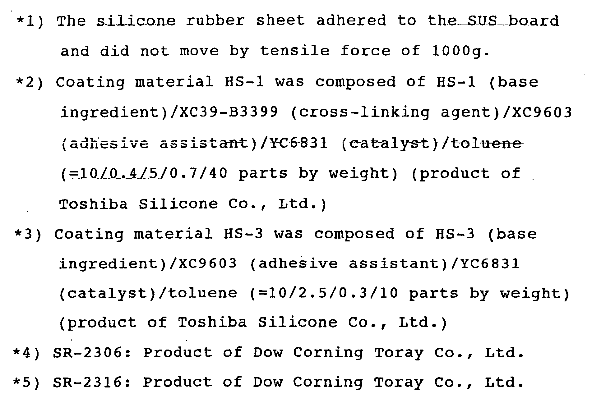
- a composition consisting of HS-3 (base ingredient) /XC9603 (adhesive assistant)/YC6831 (catalyst)/toluene ( 10/2.5/0.3/10 parts by weight) (all of them: products of Toshiba Silicone Co. Ltd.), which was a coating material for forming a non-tacky surface layer, was then applied to each of the formed protective resin layers by spray coating so as to be a coating amount of 2.0g/m 2 to form a non-tacky surface layer on each of the first and the second protective resin layers, whereby an optical circuit board of 1.9mm in thickness was fabricated.
- MU connectors were then attached on the outwardly-extended ends of the optical fibers to obtain an optical circuit board as a final product.
- the fabricated optical circuit board was pliable and flexible, since the protective resin layers were composed of a silicone rubber and a non-tacky surface layer composed of silicone-based material was formed on the surface of the silicone rubber. Furthermore, in the fabricated optical circuit board, the adhesion of the protective resin layer composed of silicone rubber to the non-tacky surface layer composed of silicone-based material was excellent but the optical circuit board did not adhere or fix to a surface of other materials such as metal, high polymer (plastic), glass, etc. Therefore, even if it contacted with a surface of other materials, the non-tacky surface layers were not damaged.
- the optical circuit board could be easily placed in a predetermined position without gaining injury. Furthermore, interconnection of it to the connectors that were attached to optical fibers extending out from other optical components could be easily carried out.
- a loss of all the interconnected optical fibers was measured. It was found to be 0.4dB or less including losses due to the insertions to the optical connectors.
- the optical circuit board so fabricated there were conducted a damp heat test (the board was left over for 5,000 hours at 75°C and 90%RH) and a heat cyclic test (-40°C to 75°C, 500 cycles). Variations and fluctuations in optical loss were both 0.5dB or less. The optical circuit boards were therefore found to be satisfactorily usable as optical interconnection apparatus.
- Optical fibers were routed on an adhesive sheet and a first protective resin layer was the formed thereof in a similar manner as in Example 1, except that a 75 ⁇ m thick release film was used instead of the PET film, and a silicone rubber coating material (product of Toshiba Silicone Co.; TSE 3033) was added dropwise and cured at 150°C for 30 minutes to form a protective resin layer, instead of using the silicone gel coating material in Example 1.
- a silicone rubber coating material product of Toshiba Silicone Co.; TSE 3033
- a second protective resin layer was formed on the back of the adhesive layer exposed. Namely, around the back of the adhesive layer, an edge-dam of 1.0mm in width and 0.5mm in height was formed with a silicone-base sealing compound (product of KONISHI CO., LTD., "BATH BOND”). A silicone rubber coating material (product of Toshiba Silicone Co. Ltd.; “TSE 3033”) was thereafter added dropwise to the inside of the edge-dam, and the silicone rubber was cured under conditions of 150°C and 30 minutes, whereby a second protective resin layer was formed.
- a silicone-base sealing compound product of KONISHI CO., LTD., "BATH BOND”
- a silicone rubber coating material product of Toshiba Silicone Co. Ltd.; "TSE 3033
- a non-tacky surface layer was then formed on each of the first and the second-protective resin layers.
- a silicone-based coating material for giving non-tackiness product of Dow Corning Toray Silicone Co., Ltd., SR2306
- SR2306 silicone-based coating material for giving non-tackiness
- MU connectors were then attached on the outwardly-extended ends of the optical fibers to obtain an optical circuit board as a final product.
- the fabricated optical circuit board was pliable and flexible, since there was no substrate and the protective resin layers were composed of a silicone rubber and a non-tacky surface layer composed of silicone-based material was formed on the surface of the silicone rubber. Furthermore, in the fabricated optical circuit board, the adhesion of the protective resin layer composed of silicone rubber to the non-tacky surface layer composed of silicone-based material was excellent but the optical circuit board did not adhere or fix to a surface of other materials such as metal, high polymer (plastic), glass, etc. Therefore, even if it contacted with a surface of other materials, the non-tacky surface layers were not damaged.
- the optical circuit board could be easily placed in a predetermined position without gaining injury. Furthermore, interconnection of it to the connectors that were attached to optical fibers extending out from other optical components could be easily carried out.
- a loss of all the interconnected optical fibers was measured. It was found to be 0.5dB or less including losses due to the insertion to the optical connectors.
- the optical circuit board so fabricated there were conducted a damp heat test (the board was left over for 5,000 hours at 75°C and 90%RH) and a heat cyclic test (-40°C to 75°C, 500 cycles). Variations and fluctuations in optical loss were both 0.4dB or less. The optical circuit boards were therefore found to be satisfactorily usable as optical interconnection apparatus.
- Example 3 Two optical circuit boards before formation of the non-tacky surface layers in Example 3 (optical circuit boards after formation of the second protective resin layer) were prepared in a similar manner as in Example 3.
- a silicone-based adhesive coating material product of Dow Corning Toray Silicone Co., Ltd., SD4592/BY24-741/SRX212
- a silicone-based adhesive coating material product of Dow Corning Toray Silicone Co., Ltd., SD4592/BY24-741/SRX212
- a non-tacky surface layer was formed respectively in a similar manner as in Example 3 to produce an optical circuit board composed of a stacked structure of 3.7mm in thickness.
- MU connectors were then attached on outwardly-extended ends of the optical fibers to obtain an optical circuit board as a final product.
- the fabricated optical circuit board was pliable and flexible, since there is no base film and the protective resin layers were composed of a silicone rubber and a non-tacky surface layer composed of silicone-based material was formed on the surface of the silicone rubber. Furthermore, in the fabricated optical circuit board, the adhesion of the protective resin layer composed of silicone rubber to the non-tacky surface layer composed of silicone-based material was excellent but the optical circuit board did not adhere or fix to a surface of other materials such as metal, high polymer (plastic), glass, etc. Therefore, even if it contacted with a surface of other materials, the non-tacky surface layers were not damaged.
- the optical circuit board could be easily placed in a predetermined position without gaining injury. Furthermore, interconnection of it to the connectors that were attached to optical fibers extending out from other optical components could be easily carried out.
- a loss of all the interconnected optical fibers was measured. It was found to be 0.5dB or less including losses due to the insertion to the optical connectors.
- the optical circuit board so fabricated there were conducted a damp heat test (the board was left over for 5,000 hours at 75°C and 90%RH) and a heat cyclic test (-40°C to 75°C, 500 cycles). Variations and fluctuations in optical loss were both 0.5dB or less.
- the optical circuit boards were therefore found to be satisfactorily usable as optical interconnection apparatus.
- the optical interconnection apparatus does not adhere or fix to the surface of other materials such as metal, high polymer (plastic), glass, etc. even if it is come into contact with them.
- a kinetic friction coefficient of the non-tacky surface layer is 3.0 or less, the effect of the present invention is remarkably exhibited.
- adhesion to the protective resin layer composed of a silicone-based material becomes more improved.
- the optical interconnection apparatus since surface strength increases as compared with the silicone-based rubber-like or gel-like material, the optical interconnection apparatus itself becomes to have an improved strength, by which the surface is not injured. Furthermore, since workability such as handling of the optical interconnection apparatus becomes easy, interconnection to other optical components is easily carried out in a limited very narrow space.
Landscapes
- Physics & Mathematics (AREA)
- General Physics & Mathematics (AREA)
- Optics & Photonics (AREA)
- Light Guides In General And Applications Therefor (AREA)
- Mechanical Coupling Of Light Guides (AREA)
Abstract
Description

Claims (11)
- (Amended) An optical interconnection apparatus which comprises a substrate, a protective resin layer composed of a silicone based rubber-like or gel-like material on one side or both sides of said substrate, and plural optical fibers which are two-dimensionally routed on the substrate so as to form a routing pattern having at least a crossing part, a curved part or a fiber pitch changing part and provided at ends thereof with end portions adapted to permit optical interconnections, and said optical fibers being held in place by said protective resin layer, wherein a non-tacky surface layer having a kinetic friction coefficient of 3 or less is provided on the surface of said protective resin layer.
- An optical interconnection apparatus according to Claim 1, wherein the non-tacky surface layer is composed of a silicone-based material.
- An optical interconnection apparatus according to Claim 2, wherein the non-tacky surface layer contains a filler.
- An optical interconnection apparatus according to Claim 1, wherein the protective resin layer is formed by filling a silicone rubber-like and/or gel-like material inside an edge-dam arranged along or in a vicinity of a peripheral edge of a substrate, a release film or another protective resin layer.
- (Deleted)
- (Amended) An optical interconnection apparatus which comprises at least two protective resin layers composed of a Silicone based rubber-like or gel-like material and plural optical fibers which are two-dimensionally routed so as to form a routing pattern having at least a crossing part, a curved part or a fiber pitch changing part and provided at ends thereof with end portions adapted to permit optical interconnections, and said optical fibers being held in place by at least one of said protective resin layers, wherein a non-tacky surface layer having a kinetic friction coefficient of 3 or less is provided on the surface of each of said protective resin layers.
- An optical interconnection apparatus according to Claim 6, wherein two or more protective resin layer are laminated via an adhesive.
- An optical interconnection apparatus according to Claim 6, wherein the non-tacky surface layer is composed of a silicone-based material.
- An optical interconnection apparatus according to Claim 8, wherein the non-tacky surface layer contains a filler.
- An optical interconnection apparatus according to Claim 6, wherein the protective resin layer is formed by filling a silicone rubber-like and/or gel-like material inside an edge-dam arranged along or in a vicinity of a peripheral edge of a substrate, a release film or another protective resin layer.
- (Deleted)
Applications Claiming Priority (3)
| Application Number | Priority Date | Filing Date | Title |
|---|---|---|---|
| JP2000126802 | 2000-04-27 | ||
| JP2000126802 | 2000-04-27 | ||
| PCT/JP2001/003612 WO2001084194A1 (en) | 2000-04-27 | 2001-04-26 | Optical connection component |
Publications (2)
| Publication Number | Publication Date |
|---|---|
| EP1286190A1 true EP1286190A1 (en) | 2003-02-26 |
| EP1286190A4 EP1286190A4 (en) | 2005-04-13 |
Family
ID=18636503
Family Applications (1)
| Application Number | Title | Priority Date | Filing Date |
|---|---|---|---|
| EP01925945A Withdrawn EP1286190A4 (en) | 2000-04-27 | 2001-04-26 | Optical connection component |
Country Status (5)
| Country | Link |
|---|---|
| US (1) | US6839475B2 (en) |
| EP (1) | EP1286190A4 (en) |
| JP (1) | JP3872984B2 (en) |
| KR (1) | KR100447673B1 (en) |
| WO (1) | WO2001084194A1 (en) |
Families Citing this family (19)
| Publication number | Priority date | Publication date | Assignee | Title |
|---|---|---|---|---|
| JP4334211B2 (en) * | 2002-12-25 | 2009-09-30 | スリーエム イノベイティブ プロパティズ カンパニー | Optical wiring sheet |
| JPWO2005088369A1 (en) * | 2004-03-16 | 2008-01-31 | 住友電気工業株式会社 | Irradiation light transmission optical fiber and light irradiation apparatus including the same |
| US7139456B2 (en) * | 2004-10-27 | 2006-11-21 | Tomoegawa Paper Co., Ltd. | Optical fiber wiring sheet and method of manufacturing same |
| US7509009B2 (en) * | 2005-03-23 | 2009-03-24 | Tomoegawa Paper Co., Ltd | Optical fiber structure and method of manufacturing same |
| US8764664B2 (en) * | 2005-11-28 | 2014-07-01 | Vizyontech Imaging, Inc. | Methods and apparatus for conformable medical data acquisition pad and configurable imaging system |
| JP4915243B2 (en) * | 2007-01-15 | 2012-04-11 | 日立電線株式会社 | Optical connector |
| US7689079B2 (en) * | 2008-01-11 | 2010-03-30 | Corning Cable Systems Llc | Optical fiber interconnection devices and systems using same |
| WO2009139292A1 (en) * | 2008-05-12 | 2009-11-19 | 財団法人山形県産業技術振興機構 | Organic el light emitting device and process for producing the organic el light emitting device |
| CA2751722A1 (en) * | 2009-02-17 | 2010-08-26 | Dow Corning Corporation | Silicone gel seal and method for its preparation and use |
| JP5174092B2 (en) * | 2009-08-31 | 2013-04-03 | 日東電工株式会社 | Adhesive film with dicing sheet and method for producing the same |
| CN103097932B (en) * | 2010-09-14 | 2015-04-15 | Fci公司 | Optical coupling device, optical system and assembly method |
| US9417418B2 (en) | 2011-09-12 | 2016-08-16 | Commscope Technologies Llc | Flexible lensed optical interconnect device for signal distribution |
| US9488788B2 (en) | 2012-09-28 | 2016-11-08 | Commscope Technologies Llc | Fiber optic cassette |
| EP2901191A4 (en) | 2012-09-28 | 2016-10-26 | Tyco Electronics Ltd Uk | MANUFACTURING AND TESTING OF CASSETTE FOR OPTICAL FIBER |
| US9223094B2 (en) | 2012-10-05 | 2015-12-29 | Tyco Electronics Nederland Bv | Flexible optical circuit, cassettes, and methods |
| WO2015161204A1 (en) * | 2014-04-17 | 2015-10-22 | Molex Incorporated | Multi-layer flexible optical circuit |
| KR102412612B1 (en) * | 2015-08-28 | 2022-06-23 | 삼성전자주식회사 | board for package and prepreg |
| MX2020002878A (en) * | 2017-10-02 | 2020-07-22 | Commscope Technologies Llc | Fiber optic circuit and preparation method. |
| US12339511B2 (en) | 2020-03-31 | 2025-06-24 | Commscope Technologies Llc | Fiber optic cable management systems and methods |
Family Cites Families (27)
| Publication number | Priority date | Publication date | Assignee | Title |
|---|---|---|---|---|
| US3715232A (en) * | 1971-07-01 | 1973-02-06 | Gte Sylvania Inc | Shatter-resistant incandescent lamp |
| US4360384A (en) * | 1975-04-09 | 1982-11-23 | Occidental Chemical Corporation | Composition for corrosion protection using metal silicides or alloys of silicon and metals |
| JPS54119691A (en) * | 1978-03-08 | 1979-09-17 | Hitachi Cable Ltd | Jumper wire |
| US4355865A (en) * | 1980-03-21 | 1982-10-26 | Amp Incorporated | Laminated optical fiber cable |
| US4770490A (en) * | 1986-08-07 | 1988-09-13 | Minnesota Mining And Manufacturing Company | Filament reinforced tape |
| US4874454A (en) * | 1987-04-24 | 1989-10-17 | Roger Laudy | Decal transfer device |
| US4936649A (en) * | 1989-01-25 | 1990-06-26 | Lymer John D | Damage evaluation system and method using optical fibers |
| US5364547A (en) * | 1989-06-09 | 1994-11-15 | The Dow Chemical Company | Lubricants containing perfluorocyclobutane rings |
| US5204925A (en) | 1991-09-11 | 1993-04-20 | At&T Bell Laboratories | Optical interconnection of circuit packs |
| US5292390A (en) * | 1992-09-30 | 1994-03-08 | At&T Bell Laboratories | Optical fiber encapsulating techniques |
| US5394504A (en) * | 1994-02-24 | 1995-02-28 | At&T Corp. | Optical fiber encapsulation techniques |
| JPH08118600A (en) * | 1994-10-26 | 1996-05-14 | Riso Kagaku Corp | Print image post-processing device |
| JP3280224B2 (en) * | 1996-02-06 | 2002-04-30 | 東レ・ダウコーニング・シリコーン株式会社 | Thermal conductive silicone gel sheet and method for producing the same |
| JPH09244536A (en) * | 1996-03-14 | 1997-09-19 | Matsushita Electric Ind Co Ltd | label |
| JPH09265019A (en) * | 1996-03-27 | 1997-10-07 | Mitsubishi Gas Chem Co Inc | Optical signal distribution device |
| DE19626514B4 (en) * | 1996-07-02 | 2007-01-18 | W.L. Gore & Associates Gmbh | Optical device with compressible laminate |
| JPH1068849A (en) * | 1996-08-29 | 1998-03-10 | Tokin Corp | Fiber optic cable |
| US6195495B1 (en) | 1997-01-17 | 2001-02-27 | Ngk Insulators, Ltd. | Optical transmitting member-holding structure |
| JP3087676B2 (en) * | 1997-02-13 | 2000-09-11 | 日本電気株式会社 | Optical coupling system and mounting structure using gel resin |
| JP3485145B2 (en) * | 1997-02-21 | 2004-01-13 | 株式会社東京パックス | Easy peeling adhesive tape |
| CA2323481C (en) * | 1998-03-12 | 2005-01-11 | Tomoegawa Paper Co., Ltd. | Optical connection component and method of producing the same |
| DE19964228B4 (en) * | 1998-09-08 | 2008-11-13 | Fujitsu Ltd., Kawasaki | Process for producing a reflection film and production of optical devices using a reflection film |
| EP1113303B1 (en) * | 1998-09-09 | 2004-07-21 | Sumitomo Electric Industries, Ltd. | Optical switch, optical fiber arrangement member, their manufacturing method, and optical fiber arranging method |
| US6350397B1 (en) * | 1999-03-10 | 2002-02-26 | Aspen Research Corporation | Optical member with layer having a coating geometry and composition that enhance cleaning properties |
| JP3794539B2 (en) * | 1999-11-30 | 2006-07-05 | 日本電信電話株式会社 | Optical fiber tape making device |
| US6547445B2 (en) * | 2001-02-06 | 2003-04-15 | Teradyne, Inc. | High-density fiber optic backplane |
| JP3699363B2 (en) * | 2001-05-15 | 2005-09-28 | Tdk株式会社 | Optical waveguide module mounting components |
-
2001
- 2001-04-26 WO PCT/JP2001/003612 patent/WO2001084194A1/en not_active Ceased
- 2001-04-26 JP JP2001581162A patent/JP3872984B2/en not_active Expired - Fee Related
- 2001-04-26 US US10/258,438 patent/US6839475B2/en not_active Expired - Fee Related
- 2001-04-26 EP EP01925945A patent/EP1286190A4/en not_active Withdrawn
- 2001-04-26 KR KR10-2002-7014382A patent/KR100447673B1/en not_active Expired - Fee Related
Also Published As
| Publication number | Publication date |
|---|---|
| US6839475B2 (en) | 2005-01-04 |
| US20030138187A1 (en) | 2003-07-24 |
| EP1286190A4 (en) | 2005-04-13 |
| KR100447673B1 (en) | 2004-09-08 |
| JP3872984B2 (en) | 2007-01-24 |
| KR20020093082A (en) | 2002-12-12 |
| WO2001084194A1 (en) | 2001-11-08 |
Similar Documents
| Publication | Publication Date | Title |
|---|---|---|
| US6839475B2 (en) | Optical connection component | |
| JPWO2001084194A1 (en) | Optical Connection Parts | |
| JP3702134B2 (en) | Manufacturing method of optical connecting parts | |
| US6567603B1 (en) | Optical interconnection apparatus and process for fabrication of the same | |
| JP3792174B2 (en) | Optical connection parts | |
| EP1182471B1 (en) | Device for optical connection | |
| WO2012134032A1 (en) | Composite sheet, and substrate for a display element using same | |
| KR100389457B1 (en) | Optical connecting component | |
| JP3356678B2 (en) | Optical connection component and method of manufacturing the same | |
| JP3326401B2 (en) | Optical connection parts | |
| JP3769165B2 (en) | Optical connecting component and method for manufacturing the same | |
| JP3326402B2 (en) | Optical connection parts | |
| JP3326397B2 (en) | Optical connection parts | |
| JP3713170B2 (en) | Optical connection parts | |
| KR20200126088A (en) | Silicone based adhesive protective film and optical member comprising the same | |
| JP2000121879A (en) | Optical connection component and method of manufacturing the same |
Legal Events
| Date | Code | Title | Description |
|---|---|---|---|
| PUAI | Public reference made under article 153(3) epc to a published international application that has entered the european phase |
Free format text: ORIGINAL CODE: 0009012 |
|
| 17P | Request for examination filed |
Effective date: 20021028 |
|
| AK | Designated contracting states |
Designated state(s): AT BE CH CY DE DK ES FI FR GB GR IE IT LI LU MC NL PT SE TR Kind code of ref document: A1 Designated state(s): AT BE CH CY DE DK ES FI FR GB GR IE IT LI LU MC NL PT SE TR |
|
| RBV | Designated contracting states (corrected) |
Designated state(s): AT BE CH DE FR GB LI |
|
| A4 | Supplementary search report drawn up and despatched |
Effective date: 20050228 |
|
| RIC1 | Information provided on ipc code assigned before grant |
Ipc: 7G 02B 6/43 B Ipc: 7G 02B 6/36 B Ipc: 7G 02B 6/00 A |
|
| 17Q | First examination report despatched |
Effective date: 20050610 |
|
| 17Q | First examination report despatched |
Effective date: 20050610 |
|
| STAA | Information on the status of an ep patent application or granted ep patent |
Free format text: STATUS: THE APPLICATION HAS BEEN WITHDRAWN |
|
| 18W | Application withdrawn |
Effective date: 20090507 |