EP1285879B1 - Verfahren um Strukturen an gegenseitigen Teilen eines Wafers zu justieren - Google Patents
Verfahren um Strukturen an gegenseitigen Teilen eines Wafers zu justieren Download PDFInfo
- Publication number
- EP1285879B1 EP1285879B1 EP02102078A EP02102078A EP1285879B1 EP 1285879 B1 EP1285879 B1 EP 1285879B1 EP 02102078 A EP02102078 A EP 02102078A EP 02102078 A EP02102078 A EP 02102078A EP 1285879 B1 EP1285879 B1 EP 1285879B1
- Authority
- EP
- European Patent Office
- Prior art keywords
- wafer
- alignment
- mask
- alignment structure
- transparent
- Prior art date
- Legal status (The legal status is an assumption and is not a legal conclusion. Google has not performed a legal analysis and makes no representation as to the accuracy of the status listed.)
- Expired - Lifetime
Links
- 238000000034 method Methods 0.000 title claims description 40
- 229910052710 silicon Inorganic materials 0.000 claims description 76
- 239000010703 silicon Substances 0.000 claims description 76
- XUIMIQQOPSSXEZ-UHFFFAOYSA-N Silicon Chemical compound [Si] XUIMIQQOPSSXEZ-UHFFFAOYSA-N 0.000 claims description 70
- WGTYBPLFGIVFAS-UHFFFAOYSA-M tetramethylammonium hydroxide Chemical compound [OH-].C[N+](C)(C)C WGTYBPLFGIVFAS-UHFFFAOYSA-M 0.000 claims description 56
- 238000007254 oxidation reaction Methods 0.000 claims description 10
- VYPSYNLAJGMNEJ-UHFFFAOYSA-N Silicium dioxide Chemical compound O=[Si]=O VYPSYNLAJGMNEJ-UHFFFAOYSA-N 0.000 claims description 9
- 239000013078 crystal Substances 0.000 claims description 9
- 230000003647 oxidation Effects 0.000 claims description 9
- 229910021420 polycrystalline silicon Inorganic materials 0.000 claims description 8
- 229920005591 polysilicon Polymers 0.000 claims description 8
- 229910052581 Si3N4 Inorganic materials 0.000 claims description 4
- 239000000377 silicon dioxide Substances 0.000 claims description 4
- 235000012239 silicon dioxide Nutrition 0.000 claims description 4
- HQVNEWCFYHHQES-UHFFFAOYSA-N silicon nitride Chemical compound N12[Si]34N5[Si]62N3[Si]51N64 HQVNEWCFYHHQES-UHFFFAOYSA-N 0.000 claims description 4
- 230000002596 correlated effect Effects 0.000 claims 1
- 230000000875 corresponding effect Effects 0.000 claims 1
- 238000000151 deposition Methods 0.000 claims 1
- 230000008021 deposition Effects 0.000 claims 1
- 230000007062 hydrolysis Effects 0.000 claims 1
- 238000006460 hydrolysis reaction Methods 0.000 claims 1
- 238000004518 low pressure chemical vapour deposition Methods 0.000 claims 1
- 238000002488 metal-organic chemical vapour deposition Methods 0.000 claims 1
- 238000000623 plasma-assisted chemical vapour deposition Methods 0.000 claims 1
- 238000004544 sputter deposition Methods 0.000 claims 1
- 235000012431 wafers Nutrition 0.000 description 132
- 229920002120 photoresistant polymer Polymers 0.000 description 30
- XLYOFNOQVPJJNP-UHFFFAOYSA-N water Substances O XLYOFNOQVPJJNP-UHFFFAOYSA-N 0.000 description 17
- 238000005530 etching Methods 0.000 description 12
- 238000004519 manufacturing process Methods 0.000 description 10
- OAKJQQAXSVQMHS-UHFFFAOYSA-N Hydrazine Chemical compound NN OAKJQQAXSVQMHS-UHFFFAOYSA-N 0.000 description 8
- KFZMGEQAYNKOFK-UHFFFAOYSA-N Isopropanol Chemical compound CC(C)O KFZMGEQAYNKOFK-UHFFFAOYSA-N 0.000 description 8
- 230000005540 biological transmission Effects 0.000 description 4
- 239000000463 material Substances 0.000 description 4
- 230000003287 optical effect Effects 0.000 description 4
- MHAJPDPJQMAIIY-UHFFFAOYSA-N Hydrogen peroxide Chemical compound OO MHAJPDPJQMAIIY-UHFFFAOYSA-N 0.000 description 3
- KWYUFKZDYYNOTN-UHFFFAOYSA-M Potassium hydroxide Chemical compound [OH-].[K+] KWYUFKZDYYNOTN-UHFFFAOYSA-M 0.000 description 3
- HEMHJVSKTPXQMS-UHFFFAOYSA-M Sodium hydroxide Chemical compound [OH-].[Na+] HEMHJVSKTPXQMS-UHFFFAOYSA-M 0.000 description 3
- 230000015572 biosynthetic process Effects 0.000 description 3
- 238000003754 machining Methods 0.000 description 3
- 239000004065 semiconductor Substances 0.000 description 3
- 239000000126 substance Substances 0.000 description 3
- VHUUQVKOLVNVRT-UHFFFAOYSA-N Ammonium hydroxide Chemical compound [NH4+].[OH-] VHUUQVKOLVNVRT-UHFFFAOYSA-N 0.000 description 2
- WMFOQBRAJBCJND-UHFFFAOYSA-M Lithium hydroxide Chemical compound [Li+].[OH-] WMFOQBRAJBCJND-UHFFFAOYSA-M 0.000 description 2
- 239000000908 ammonium hydroxide Substances 0.000 description 2
- HUCVOHYBFXVBRW-UHFFFAOYSA-M caesium hydroxide Chemical compound [OH-].[Cs+] HUCVOHYBFXVBRW-UHFFFAOYSA-M 0.000 description 2
- YCIMNLLNPGFGHC-UHFFFAOYSA-N catechol Chemical compound OC1=CC=CC=C1O YCIMNLLNPGFGHC-UHFFFAOYSA-N 0.000 description 2
- 230000004438 eyesight Effects 0.000 description 2
- 238000002955 isolation Methods 0.000 description 2
- 238000000059 patterning Methods 0.000 description 2
- CPRMKOQKXYSDML-UHFFFAOYSA-M rubidium hydroxide Chemical compound [OH-].[Rb+] CPRMKOQKXYSDML-UHFFFAOYSA-M 0.000 description 2
- 229910000838 Al alloy Inorganic materials 0.000 description 1
- QGZKDVFQNNGYKY-UHFFFAOYSA-N Ammonia Chemical compound N QGZKDVFQNNGYKY-UHFFFAOYSA-N 0.000 description 1
- RYGMFSIKBFXOCR-UHFFFAOYSA-N Copper Chemical compound [Cu] RYGMFSIKBFXOCR-UHFFFAOYSA-N 0.000 description 1
- 238000000018 DNA microarray Methods 0.000 description 1
- PIICEJLVQHRZGT-UHFFFAOYSA-N Ethylenediamine Chemical compound NCCN PIICEJLVQHRZGT-UHFFFAOYSA-N 0.000 description 1
- UFHFLCQGNIYNRP-UHFFFAOYSA-N Hydrogen Chemical compound [H][H] UFHFLCQGNIYNRP-UHFFFAOYSA-N 0.000 description 1
- ZOKXTWBITQBERF-UHFFFAOYSA-N Molybdenum Chemical compound [Mo] ZOKXTWBITQBERF-UHFFFAOYSA-N 0.000 description 1
- NRTOMJZYCJJWKI-UHFFFAOYSA-N Titanium nitride Chemical compound [Ti]#N NRTOMJZYCJJWKI-UHFFFAOYSA-N 0.000 description 1
- 150000008044 alkali metal hydroxides Chemical class 0.000 description 1
- 150000001412 amines Chemical class 0.000 description 1
- 238000004458 analytical method Methods 0.000 description 1
- QVGXLLKOCUKJST-UHFFFAOYSA-N atomic oxygen Chemical compound [O] QVGXLLKOCUKJST-UHFFFAOYSA-N 0.000 description 1
- 238000004364 calculation method Methods 0.000 description 1
- 230000000295 complement effect Effects 0.000 description 1
- 239000002872 contrast media Substances 0.000 description 1
- 229910052802 copper Inorganic materials 0.000 description 1
- 239000010949 copper Substances 0.000 description 1
- 230000000694 effects Effects 0.000 description 1
- 230000003628 erosive effect Effects 0.000 description 1
- 239000001257 hydrogen Substances 0.000 description 1
- 229910052739 hydrogen Inorganic materials 0.000 description 1
- 238000003331 infrared imaging Methods 0.000 description 1
- 239000007791 liquid phase Substances 0.000 description 1
- 230000005226 mechanical processes and functions Effects 0.000 description 1
- QSHDDOUJBYECFT-UHFFFAOYSA-N mercury Chemical compound [Hg] QSHDDOUJBYECFT-UHFFFAOYSA-N 0.000 description 1
- 229910052753 mercury Inorganic materials 0.000 description 1
- 239000007769 metal material Substances 0.000 description 1
- 229910044991 metal oxide Inorganic materials 0.000 description 1
- 150000004706 metal oxides Chemical class 0.000 description 1
- 229910052750 molybdenum Inorganic materials 0.000 description 1
- 239000011733 molybdenum Substances 0.000 description 1
- 229910021421 monocrystalline silicon Inorganic materials 0.000 description 1
- 231100000252 nontoxic Toxicity 0.000 description 1
- 230000003000 nontoxic effect Effects 0.000 description 1
- 239000001301 oxygen Substances 0.000 description 1
- 229910052760 oxygen Inorganic materials 0.000 description 1
- 229910021332 silicide Inorganic materials 0.000 description 1
- 150000003376 silicon Chemical class 0.000 description 1
- 229910052814 silicon oxide Inorganic materials 0.000 description 1
- 229940073455 tetraethylammonium hydroxide Drugs 0.000 description 1
- LRGJRHZIDJQFCL-UHFFFAOYSA-M tetraethylazanium;hydroxide Chemical compound [OH-].CC[N+](CC)(CC)CC LRGJRHZIDJQFCL-UHFFFAOYSA-M 0.000 description 1
- MAKDTFFYCIMFQP-UHFFFAOYSA-N titanium tungsten Chemical compound [Ti].[W] MAKDTFFYCIMFQP-UHFFFAOYSA-N 0.000 description 1
- WFKWXMTUELFFGS-UHFFFAOYSA-N tungsten Chemical compound [W] WFKWXMTUELFFGS-UHFFFAOYSA-N 0.000 description 1
- 229910052721 tungsten Inorganic materials 0.000 description 1
- 239000010937 tungsten Substances 0.000 description 1
Images




Classifications
-
- B—PERFORMING OPERATIONS; TRANSPORTING
- B81—MICROSTRUCTURAL TECHNOLOGY
- B81C—PROCESSES OR APPARATUS SPECIALLY ADAPTED FOR THE MANUFACTURE OR TREATMENT OF MICROSTRUCTURAL DEVICES OR SYSTEMS
- B81C99/00—Subject matter not provided for in other groups of this subclass
- B81C99/0055—Manufacturing logistics
- B81C99/007—Marking
-
- B—PERFORMING OPERATIONS; TRANSPORTING
- B81—MICROSTRUCTURAL TECHNOLOGY
- B81C—PROCESSES OR APPARATUS SPECIALLY ADAPTED FOR THE MANUFACTURE OR TREATMENT OF MICROSTRUCTURAL DEVICES OR SYSTEMS
- B81C1/00—Manufacture or treatment of devices or systems in or on a substrate
- B81C1/00388—Etch mask forming
- B81C1/00396—Mask characterised by its composition, e.g. multilayer masks
-
- B—PERFORMING OPERATIONS; TRANSPORTING
- B81—MICROSTRUCTURAL TECHNOLOGY
- B81C—PROCESSES OR APPARATUS SPECIALLY ADAPTED FOR THE MANUFACTURE OR TREATMENT OF MICROSTRUCTURAL DEVICES OR SYSTEMS
- B81C1/00—Manufacture or treatment of devices or systems in or on a substrate
- B81C1/00388—Etch mask forming
- B81C1/00404—Mask characterised by its size, orientation or shape
-
- Y—GENERAL TAGGING OF NEW TECHNOLOGICAL DEVELOPMENTS; GENERAL TAGGING OF CROSS-SECTIONAL TECHNOLOGIES SPANNING OVER SEVERAL SECTIONS OF THE IPC; TECHNICAL SUBJECTS COVERED BY FORMER USPC CROSS-REFERENCE ART COLLECTIONS [XRACs] AND DIGESTS
- Y10—TECHNICAL SUBJECTS COVERED BY FORMER USPC
- Y10S—TECHNICAL SUBJECTS COVERED BY FORMER USPC CROSS-REFERENCE ART COLLECTIONS [XRACs] AND DIGESTS
- Y10S438/00—Semiconductor device manufacturing: process
- Y10S438/975—Substrate or mask aligning feature
Definitions
- This invention relates to the field of micro structure fabrication, and in particular to a method of aligning microstructures on opposite sides of a wafer.
- MEMS Micro-Electro-Mechanical Systems
- Special alignment systems capable of back side alignment are used to perform the alignment of structures located on the front side of a silicon wafer to structures located on the back side of the same silicon wafer as to ensure proper machining of MEMS.
- These special systems use split field optics and/ or through-the-silicon-wafer infrared imaging to perform 1X direct contact alignment or 1X proximity contact alignment of the structures on both sides of the silicon wafer.
- One example of a prior art alignment system is the MA1006 contact aligner manufactured by K&W Gmbh. This system is capable of handling 1X masks of sizes of up to 7"x7" and silicon wafers of up to 6" diameter.
- the transfer of a 1X mask located on the back side of the silicon wafer into the photoresist also located on the back side of this silicon wafer while aligning this transferred 1X photoresist pattern to the structures already located on the front side of the same silicon wafer is carried out by first illuminating the 1X mask located on the back side of the silicon wafer with an intense infrared light not absorbed by the photoresist also located on the back side of the silicon wafer.
- the dynamic alignment of the 1X mask closely positioned against the photoresist coated back side of the silicon wafer and the structures located on the front side of the same silicon wafer is observed using the image transmitted through a 5X-35X zooming microscope objective and captured from the Charge-Coupled-Device (CCD) infrared sensor of a Hamamatsu alignment camera a resulting infrared imaged magnified by 150X - 1000X zoom on a Sony 14" Monitor.
- the 1X mask and the photoresist coated back side of the silicon wafer are contacted with more or less pressure (0.03 N/ cm 2 - 0.16 N/ cm 2 ) when proper alignment is achieved.
- the photoresist coated on the back side of the silicon wafer is exposed with ultra-violet light of 240 nm - 450 nm wavelength to transfer the pattern of the 1X mask into the photoresist.
- the resulting alignment of the already existing pattern located on the front side and of the newly transferred 1X pattern into the photoresist of the back side of the wafer is claimed to be of the order of 1 ⁇ m.
- the MA6 contact aligner manufactured by the company Karl Suss, also of Germany.
- This system is also capable of handling 1X masks of sizes of up to 7"x7" and silicon wafers of up to 6" diameter.
- the 1X mask on the back side of the silicon wafer is first illuminated with infrared light.
- the alignment of the 1X mask near the back side and the structures of the front side of the silicon wafer are observed using the image transmitted through a 10X microscope objective.
- the 1X mask and the photoresist coated back side of the silicon wafer are contacted with more or less pressure when proper alignment is achieved.
- the photoresist coated on the back side of the silicon wafer is exposed with ultra-violet light as to transfer the pattern of the 1X mask into the photoresist.
- optical resolution of the transferred pattern into the photoresist is claimed to be of the order of 1 ⁇ m when using vacuum contact between the 1X mask and the photoresist.
- the contact aligner also manufactured by Karl Suss. Unlike the MA6 aligner, which is capable of aligning wafers of up to 6" in diameter, the MJB 3 UV400 IR 6 contact aligner is only capable of handling 1X masks of sizes of up to 4"x4" and silicon wafers of up to 3".
- the 1X mask on the back side of the silicon wafer is first illuminated with infrared light. Using a splitfield Vidicon video camera and through infrared transmission, the alignment of the 1X mask near the back side and the structures of the front side of the silicon wafer is observed using the image transmitted through a 10X microscope objective. The 1X mask and the photoresist coated back side of the silicon wafer are contacted with more or less pressure when proper alignment is achieved. Finally, the photoresist coated on the back side of the silicon wafer is exposed with ultra-violet light as to transfer the pattern of the 1X mask into the photoresist.
- optical resolution of the transferred pattern into the photoresist is also claimed to be of the order of 1 ⁇ m when using vacuum contact between the 1X mask and the photoresist.
- the EV620 contact aligner manufactured by the company Electronic Visions is also capable of handling 1X masks of sizes of up to 7"x7" and silicon wafers of up to 6" diameter.
- the 1X mask on the back side of the silicon wafer is first illuminated.
- the alignment of the 1X mask near the back side and the structures of the front side of the silicon wafer is observed using the image transmitted through a 3.6X, 4X, 5X, 10X or 20X objective equipped with digital Zoom.
- the 1X mask and the photoresist coated back side of the silicon wafer are contacted with more or less pressure (0.5 N to 40N) when proper alignment is achieved.
- the photoresist coated on the back side of the silicon wafer is exposed with ultra-violet light to transfer the pattern of the 1X mask into the photoresist.
- the alignment accuracy between the transferred patterns into the photoresist of the back side and the patterns of the front side is claimed to be better then about 1 ⁇ m.
- the OAI 5000 contact aligner manufactured by the company Optics Automation Instrumentation is capable of handling 1X masks of sizes of up to 9"x9" and silicon wafers of up to 8" diameter.
- the 1X mask on the back side of the silicon wafer is illuminated with infrared light.
- the alignment of the 1X mask near the back side and the structures of the front side of the silicon wafer is observed using the image transmitted through a 6X or 32X objective.
- the 1X mask and the photoresist coated back side of the silicon wafer are contacted with more or less vacuum (2 to 15 inch of mercury) when proper alignment is achieved.
- the photoresist coated on the back side of the silicon wafer is exposed with ultraviolet light to transfer the pattern of the 1X mask into the photoresist.
- optical resolution of the transferred pattern into the photoresist is claimed to be 0.73 ⁇ m when using 365nm i-line exposure of the 1X mask into suitable photoresist.
- a method of aligning structures on front and rear sides of a silicon wafer for a MEMS device wherein an alignment structure is formed on the front side of the wafer, an anisotropic etch is performed on the rear side of the wafer to form a window opening through which the alignment structure is visible, and precise alignment is carried out on the alignment structure, characterized in that part of the bulk of the wafer is converted on the front side of the wafer to form at least one transparent island of silicon dioxide at an alignment location, the transparent island having an exposed front side and a rear side embedded in the wafer, the anisotropic etch substantially reaches the rear side of the transparent island, the alignment structure (18') is provided on the exposed front side of the transparent island (16), and the precise alignment is carried out on the alignment structure through the transparent island.
- the invention may employ a special manufacturing technique which uses the crystal properties of the silicon wafer to permit the fabrication of thin transparent oxide islands on its front side over which opaque alignment structures are positioned in such a way to be visible through openings which are wet-etched through the surface of the back side and up to the bottom surface of this transparent oxide island.
- the alignment of the pattern-to-be-transferred on the back side of the facing down silicon wafer can be carried out using standard 5X Canon wafer stepper by aligning the alignment structures of the mask of the pattern-to-be-transferred to the alignment structures already located on the upper surface of the transparent oxide island.
- alignment marks There can be one large island with several alignment marks, but more usually several smaller islands will be formed, each bearing one or more alignment marks.
- the openings on the rear side of the wafer should normally reach the transparent islands, although the invention will still work so long as they extend sufficiently far to permit the alignment structures to be visible through the openings from the rear side of the wafer.
- the transparent islands are preferably made using a local oxidation of silicon (LOCOS) sequence in a MEMS process as to allow the fabrication of oxide islands on the front side of the wafer. These can then act as an etch stop layer during etching of the openings, which form observation windows, from the rear side of the wafer at a later step of the process.
- LOC local oxidation of silicon
- the alignment structures can be patterned over these oxide islands using a standard Canon 5X wafer stepper so as to be visible from the rear side of the wafer through the underlying oxide islands and through the observation windows which can be etched from the rear side of the wafer at a later step of the process.
- a chemical solution is used to transfer a first poorly aligned thermal oxide hard mask using the major flat and the edges of the silicon wafer as the positioning reference.
- This hard mask is used to open coarsely aligned observation windows with this chemical solution which performs an anisotropic etching along some crystallographic planes from the back side and all the way through the 625 ⁇ m thick silicon wafer as to reach the oxide islands. These observation windows allow the observation of the alignment structures of the front side of the wafer from the back side of the wafer.
- the alignment structures of the mask to be aligned on the back side of the wafer can then be properly aligned through these coarsely aligned observation windows with their corresponding alignment structures located over the grown oxide island on the front side of the wafer using a standard 5X Canon wafer stepper.
- the transferred patterns on the back side of the wafer can also include other alignment marks which can allow shot-by-shot alignment of the remaining masks to be transferred to the back side of the wafer.
- Single crystal silicon wafers have the face-centered cubic crystal structure shown in Figure 1 .
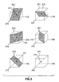
- Face-centered cubic crystals are characterized by a series of Six ⁇ 100 ⁇ orientation planes shown in Figure 2 ; six ⁇ 110 ⁇ orientation planes, as shown in Figure 3 ; and four ⁇ 111 ⁇ orientation planes shown in Figure 4 .
- the etch rate ratio is used to quantify the anisotropic behavior of these solutions.
- the etch rate ratio is defined as (Etch rate of ⁇ 100 ⁇ planes)/ (Etch rate of ⁇ 111 ⁇ planes).
- Tetramethylammonium hydroxide (TMAOH) solution in water is a suitable substance because it is non-toxic, can be handled easily, is compatible with Complementary Metal Oxide Semiconductor, CMOS, processes, and because TMAOH and water solutions do not decompose below 130°C.
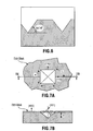
- Figures 7a and 7b show that the anisotropic etching of ⁇ 100 ⁇ oriented silicon wafers in a TMAOH solution using a ⁇ 110 ⁇ oriented square mask of size (a x a) results in an inverted square pyramid defined by four ⁇ 111 ⁇ planes oriented at 54.74° with respect to the wafer surface.
- the inverted pyramid typically has a depth of about 0.5 x a ⁇ 2 into the silicon.
- Figures 8a and 8b show that an anisotropic etch performed all the way through ⁇ 100 ⁇ oriented silicon wafers of thickness c in a TMAOH solution using a ⁇ 110 ⁇ oriented rectangular mask of size (a x b) results in an inverted and sloped rectangular via hole of bottom size ( d x e ) defined by four ⁇ 111 ⁇ planes oriented at 54.74° with respect to the wafer surface.
- Figures 9a and 9b show that the anisotropic etch performed all the way through ⁇ 100 ⁇ oriented silicon wafers of thickness c in a TMAOH solution using an arbitrary shaped mask of external size ( a x b ) as measured using ⁇ 110 ⁇ directions also results in an inverted and sloped rectangular via hole of bottom size ( d x e ) defined by four ⁇ 111 ⁇ planes oriented at 54.74° with respect to the wafer surface.
- the relationships between the ( a x b ) size of the mask, the c thickness of the wafer, and the ( d x e ) bottom size of the sloped rectangular via hole remain the same as above.
- FIG 10 shows the LOCal Oxydation of Silicon (LOCOS) process resulting in the fabrication of oxide islands on the front side of the wafer.
- LOCOS isolation process uses oxygen at high temperature to locally convert the silicon which is unprotected by silicon nitride to silicon oxide.
- the LOCOS process sequence is integrated in the complete MEMS process and allows the local growth of thermal oxide at unprotected locations of the front side of the wafer.
- the oxide islands are used as an etch stop layer which stops the etching action of TMAOH at a later step in the process.
- a silicon nitride layer 12 is deposited on the (100) face partially processed wafer 10.
- the mask 12 is patterned to form openings 14 exposing the underlying silicon.
- a thermal oxidation step of the underlying silicon is then carried out to form transparent silicon dioxide islands 16. This step is followed by removal of the silicon nitride mask to leave the transparent oxide islands 16.
- Thermal oxidation temperatures are typically between 900 and 1200°C.
- Figure 11 shows the process resulting in the patterning of alignment structures wafer using a standard 5X Canon wafer stepper over the oxide islands of the front side of the wafer.
- These high resolution alignment structures are made of an opaque material such as polysilicon which will be used as a contrast material when observed from the back side of the wafer through the underlying oxide island and through an observation window which will be etched from the back side of the wafer using TMAOH.
- a polysilicon layer 18 is deposited over the oxide islands 16.
- a photoresist 20 is applied and patterned to leave exposed polysilicon 18. This is subsequently etched away and the residual photoresist 20 removed to leave the alignment structures 18' formed of the residual polysilicon.
- Figure 12 is an example showing three high resolution alignment structures to be patterned over the oxide islands on the front side of the wafer using a standard 5X Canon wafer stepper.
- Each one of the three alignment structures of the triplet of alignment structures is located on an independent oxide island to maximize their spacing, thus maximizing the alignment accuracy, and to minimize the total area of the observation windows to be opened from the back side of the wafer so as to minimize the risk of oxide island perforation under the action of the vaccum chuck holding the wafer in position during alignment.
- Figure 13 is an example showing the position of triplets of alignment structures on a ⁇ 100 ⁇ silicon wafer using a standard 5X Canon wafer stepper.
- This figure shows that the boundaries of the oxide islands are outside and farther away from the rectangular boundaries of the alignment structures with a minimum overlap in each directions of about 100 ⁇ m.
- This minimum overlap is about 100 ⁇ m because the blind positioning of the back side mask which allows the opening of the various observation windows has a tolerance of about ⁇ 60 ⁇ m in all directions when the major flat and the edge of the wafer are used for reference.
- This overlap ensures that the top of the TMAOH etched observation windows will not reach a point outside their respective oxide islands.
- High performance back side alignment is then possible using the transparent oxide islands and the visible-from-the-back-side alignment structures through the observation window.
- Figure 14 shows the process resulting in the patterning of the observation windows from the back side of a ⁇ 100 ⁇ silicon wafer using a standard 5X Canon wafer stepper.
- the results show that a thermal oxide hard mask is etched at about 3.5 nm/ hour with the described TMAOH solution. Since the etching of the 625 ⁇ m thick and ⁇ 100 ⁇ oriented silicon wafer at a rate of about 27.7 ⁇ m/ hour will be completed in about 22.6 hours, the hard mask etch rate ratio of about 8000:1 reduces the hard mask consumption to about 80nm.
- the hard mask used to pattern the observation window has to be properly sized to compensate for the 54.74° slope shown in Figure 8 over a complete wafer thickness of about 625 ⁇ m.
- Figure 15 shows an example of two alignment structures present on the mask to be aligned on the back side of the wafer a standard 5X Canon wafer stepper.
- Each one of the two alignment structures of the doublet of alignment structures is to be aligned on the back side of the wafer through its corresponding grown oxide island to its corresponding alignment structure of the triplet present on the other side of its corresponding grown oxide island present on the front side of the wafer.
- Figure 16 is an example showing the alignment of doublets of the mask aligned on the back side of a ⁇ 100 ⁇ silicon wafer to the visible-from-the-back-side triplets observed through the oxide of misaligned observation windows a standard 5X Canon wafer stepper.
- This Figure shows that even if the blind positioning of the back side mask that allowed the opening of the various observation windows resulted in a misalignment of the observation windows by up to about ⁇ 60 ⁇ m in all directions when simply using the major flat and the edge of the wafer for alignment, proper back side alignment is possible because the doublets can be aligned through the oxide island and the observation window to the visible-from-the-back-side triplets.
- the sequence for back side alignment is as follows: First, a standard 5X Canon wafer stepper finds the optimum alignment of the first doublet. It looks for the first pre-alignment cross (structure 2), then aligns the right pair of chevrons of the front side (structure 3) to the right chevron of the 5X mask (structure 5) and the left pair of chevrons of the front side (structure 1) and the left chevron of the 5X mask (structure 4) and then records the relative position of the 5X mask and of the wafer.
- the 5X Canon wafer stepper finds the optimum alignment of the second , third and fourth doublets using the same procedure and again records the relative position of the mask and of the wafer for these three other locations.
- the 5X Canon wafer stepper then calculates the best relative position using the four relative positions and prints the pattern to be transferred, shot-by-shot and in the focal plane of the back side of the wafer so as to cover the whole wafer surface with the patterns to be transferred to the back side of the wafer.
- the transferred patterns on the back side of the wafer can include other alignment marks which can be used to align shot-by-shots the remaining masks to be transferred to the back side of the wafer.
- the 25wt% TMAOH in water solution could have a different concentration ranging from 0.5wt% TMAOH in water to 50wt% in water.
- the temperature of the TMAOH/water solutions could be different than 80°C ranging from 60°C to 130°C.
- Isopropyl alcohol (IPA) could be added to the TMAOH/water solutions up to 20 vol% as to modify the anisotropic etch properties of the solution and improve the etching characteristics of P-Type silicon.
- (CH 3 ) 4 NOH could be added to the TMAOH/water solutions up to 30 vol% so as to modify the anisotropic etch properties of the solution and the selectivity to the hard masks.
- Hydrogen peroxide H 2 O 2
- H 2 O 2 could be added to the TMAOH/water solutions up to 10vol% as to prevent the formation of hillocks and to use its oxidation potential to prevent the formation of hydrogen bubbles during etching.
- Silicon could be added to the TMAOH/water solutions to dope it.
- TMAOH could be replaced in the upper solutions by tetraethylammonium hydroxide, TEAOH; an alkali metal hydroxide, such as: KOH, NaOH, LiOH, RbOH or CsOH; by ammonium hydroxide, thus forming and ammonium hydroxide and water (AHW) solution; or by various hydrazine solutions such as hydrazine/water, hydrazine/polycatechol, hydrazine/isopropanol/water; by Ethylenediamine/ pyrocatechol/water solutions or amine gallates solutions.
- TEAOH tetraethylammonium hydroxide
- an alkali metal hydroxide such as: KOH, NaOH, LiOH, RbOH or CsOH
- ammonium hydroxide thus forming and ammonium hydroxide and water (AHW) solution
- AHW ammonium hydroxide and water
- various hydrazine solutions such as
- the size of the various alignment structures of a given alignment mark is small enough, or if the oxide island is strong enough, it is possible to group the alignment structures of the alignment mark on a single island and to have only one observation window to reach this alignment mark from the back side of the wafer.
- the described process uses a standard 5X Canon wafer stepper.
- This equipment may be replaced, for example, by a 20X wafer stepper; a 10X wafer stepper; a 1X proximity aligner; or a 1X contact aligner.
- the Canon equipment could be replaced by other exposure equipment manufactured by another manufacturer, such as Nikon, ASML; Ultratech; Perkin Elmer; Silicon Valley Group; Karl Suss; Electronic Vision; K&W Gmbh; Optics Automation Instrumentation.
- the number of alignment marks (Left chevron structure, pre-alignment structure and right chevron structure) can be different then the proposed four.
- the minimum number is about two and the maximum number is about 1000.
- the position of the alignment marks can be different then the examples.
- the alignment marks can be different than the proposed set of left chevron, pre-alignment and right chevron.
- the alignment equipment type, the equipment manufacturer or the user's requirements will dictate the design of the alignment marks.
- the proposed polysilicon material can be replaced by another opaque material such as other semiconductor materials such as doped polysilicon, silicides or polycides; and metallic materials such as aluminum alloys, copper, molybdenum, tungsten, titanium-tungsten, titanium nitride.
- the simultaneous alignment of all alignment marks indicates optimum alignment and there is no need to record the relative position of the mask and of the wafer and to perform a calculation of the optimum position.
- the boundaries of the oxide islands are outside and farther away from the rectangular boundaries of the alignment structures with a proposed minimum overlap in each directions of about 100 ⁇ m. If the blind alignment of the back of the wafer using the major flat or the edges of the wafer or other means provides a better tolerance then the mentioned ⁇ 60 ⁇ m in all directions, it would be possible to reduce the proposed overlap of 100 ⁇ m to a lower value and still prevent the top of the TMAOH etched observation windows to not reach a point outside their respective oxide islands.
- the thickness of the hard mask can be very different from the proposed 80nm so as to prevent the total erosion of hard mask during the etching of the observation windows.
- the main application of the invention is in the manufacturing of Micro-Electro-Mechanical Systems (MEMS), thus integrating electronics functions and mechanical functions. Optics functions can also be integrated so as to achieve the fabrication of Micro -Opto- Electro-Mechanical Systems (MOEMS). Biological or medical functions can also be integrated as to achieve microfluidics devices such as biochips, laboratopry-on-a-chip (LOAC) or micro-total analysis systems ( ⁇ -TAS).
- MEMS Micro-Electro-Mechanical Systems
- Optics functions can also be integrated so as to achieve the fabrication of Micro -Opto- Electro-Mechanical Systems (MOEMS).
- Biological or medical functions can also be integrated as to achieve microfluidics devices such as biochips, laboratopry-on-a-chip (LOAC) or micro-total analysis systems ( ⁇ -TAS).
- LOAC laboratopry-on-a-chip
- ⁇ -TAS micro-total analysis systems
- This described process provides a special manufacturing technique which prevents the use of these special alignment systems and which allows the use of standard high performance steppers capable of better resolutions with 5X masks.
Landscapes
- Engineering & Computer Science (AREA)
- Manufacturing & Machinery (AREA)
- Microelectronics & Electronic Packaging (AREA)
- Exposure And Positioning Against Photoresist Photosensitive Materials (AREA)
- Container, Conveyance, Adherence, Positioning, Of Wafer (AREA)
Claims (17)
- Verfahren zum Ausrichten von Strukturen an der Vorder- und Hinterseite eines Siliciumwafers für ein MEMS-Element, wobei eine Ausrichtungsstruktur (18') an der Vorderseite des Wafers (10) gebildet wird, wobei ein anisotropisches Ätzen an der Hinterseite des Wafers (10) durchgeführt wird, um eine Fensteröffnung zu bilden, durch die die Ausrichtungsstruktur (18') sichtbar ist, und wobei eine genaue Ausrichtung bei der Ausrichtungsstruktur (18') vorgenommen wird, dadurch gekennzeichnet, dass ein Teil des Grundmaterials des Wafers (10) an der Vorderseite des Wafers umgewandelt wird, um mindestens eine transparente Insel (16) aus Siliciumdioxid an einer Ausrichtungsstelle zu bilden, wobei die transparente Insel (16) eine freigelegte Vorderseite und eine Hinterseite aufweist, eingebettet im Wafer (10), wobei das anisotropische Ätzen im Wesentlichen die Hinterseite der transparenten Insel (16) erreicht, wobei die Ausrichtungsstruktur (18') an der freigelegten Vorderseite der transparenten Insel (16) bereitgestellt wird, und wobei die genaue Ausrichtung bei der Ausrichtungsstruktur (18') durch die transparente Insel (16) vorgenommen wird.
- Verfahren nach Anspruch 1, bei dem die mindestens eine transparente Insel (16) als ein Ätzstopp wirkt.
- Verfahren nach Anspruch 1 oder 2, bei dem der Wafer (10) eine kubisch-flächenzentrierte Kristallstruktur aufweist.
- Verfahren nach Anspruch 1 oder 2, bei dem der Wafer (10) in einer {100} Ebene ausgerichtet ist, und bei dem das anisotropische Ätzen durch eine {110} ausgerichtete Maske durchgeführt wird, um eine umgekehrte pyramidenförmige Öffnung zu bilden, die durch vier {111} Ebenen definiert wird.
- Verfahren nach einem der vorhergehenden Ansprüche, bei dem das anisotropische Ätzen mit einer Lösung von Tetramethylammoniumhydroxid durchgeführt wird.
- Verfahren nach einem der vorhergehenden Ansprüche, bei dem das Siliciumdioxid durch lokale Oxidation des Siliciumwafers (10) gebildet wird.
- Verfahren nach Anspruch 6, bei dem die lokale Oxidation mittels thermischer Oxidation durchgeführt wird.
- Verfahren nach Anspruch 7, bei dem die thermische Oxidation durch eine Siliciumnitrid-Maske (12) durchgeführt wird.
- Verfahren nach einem der vorhergehenden Ansprüche, bei dem die mindestens transparente Insel (16) mittels eines Verfahrens hergestellt wird, das aus der Gruppe ausgewählt wird, die besteht aus: PECVD, LPCVD, MOCVD, Elektronenzyklotronresonanzabscheidung, Hochfrequenzsputtering und Flammenhydrolyse.
- Verfahren nach einem der vorhergehenden Ansprüche, das eine Vielzahl der transparenten Inseln (16) aufweist, wobei eine jede mindestens eine Ausrichtungsstruktur (18') trägt.
- Verfahren nach Anspruch 10, das ein einzelnes transparentes Fenster aufweist, das eine Vielzahl von Ausrichtungsstrukturen (18') trägt.
- Verfahren nach einem der vorhergehenden Ansprüche, bei dem die Ausrichtungsstruktur (18') durch Ausbilden einer undurchsichtigen Ausrichtungsmarkierung auf der mindestens einen transparenten Insel (16) gebildet wird.
- Verfahren nach einem der vorhergehenden Ansprüche, bei dem die mindestens eine Ausrichtungsstruktur (18') aus der Gruppe ausgewählt wird, die aus einem Kreuz und Winkeln besteht.
- Verfahren nach einem der vorhergehenden Ansprüche, bei dem die mindestens eine Ausrichtungsstruktur (18') aus Polysilicium besteht.
- Verfahren nach einem der vorhergehenden Ansprüche, bei dem eine harte Maske auf der Hinterseite des Wafers (10) gebildet wird, wobei die harte Maske eine entsprechende Öffnung aufweist, die der oder einer jeden transparenten Insel (16) entspricht, und wobei die oder eine jede Öffnung im Wesentlichen gebildet wird, indem ein anisotropisches Ätzen durch die harte Maske durchgeführt wird.
- Verfahren nach Anspruch 15, bei dem die harte Maske aus thermischem Oxid hergestellt wird.
- Verfahren nach einem der vorhergehenden Ansprüche, bei dem nach dem Schritt des Durchführens der genauen Ausrichtung bei der Ausrichtungsstruktur (18') auf der Vorderseite des Wafers (10) durch die transparente Insel (16) mindestens eine zweite Ausrichtungsstruktur, die mit der mindestens einen Ausrichtungsstruktur (18') auf der Vorderseite des Wafers (10) in Wechselbeziehung steht, auf der Hinterseite des Wafers (10) für eine Verwendung bei der anschließenden Verarbeitung auf der Hinterseite des Wafers (10) gebildet wird.
Applications Claiming Priority (2)
| Application Number | Priority Date | Filing Date | Title |
|---|---|---|---|
| US923367 | 2001-08-08 | ||
| US09/923,367 US6555441B2 (en) | 2001-08-08 | 2001-08-08 | Method of aligning structures on opposite sides of a wafer |
Publications (3)
| Publication Number | Publication Date |
|---|---|
| EP1285879A2 EP1285879A2 (de) | 2003-02-26 |
| EP1285879A3 EP1285879A3 (de) | 2005-02-09 |
| EP1285879B1 true EP1285879B1 (de) | 2009-10-28 |
Family
ID=25448565
Family Applications (1)
| Application Number | Title | Priority Date | Filing Date |
|---|---|---|---|
| EP02102078A Expired - Lifetime EP1285879B1 (de) | 2001-08-08 | 2002-07-31 | Verfahren um Strukturen an gegenseitigen Teilen eines Wafers zu justieren |
Country Status (3)
| Country | Link |
|---|---|
| US (1) | US6555441B2 (de) |
| EP (1) | EP1285879B1 (de) |
| DE (1) | DE60234148D1 (de) |
Families Citing this family (14)
| Publication number | Priority date | Publication date | Assignee | Title |
|---|---|---|---|---|
| US7113258B2 (en) * | 2001-01-15 | 2006-09-26 | Asml Netherlands B.V. | Lithographic apparatus |
| US6768539B2 (en) * | 2001-01-15 | 2004-07-27 | Asml Netherlands B.V. | Lithographic apparatus |
| JP2002289507A (ja) * | 2001-03-28 | 2002-10-04 | Sanyo Electric Co Ltd | 半導体装置の製造方法 |
| JP2005064068A (ja) * | 2003-08-19 | 2005-03-10 | Renesas Technology Corp | 半導体装置及びその製造方法 |
| US20070073448A1 (en) * | 2003-08-19 | 2007-03-29 | Renesas Technology Corp. | Semiconductor device having a hole or a step of normal mesa shape as viewed from any cross-section and manufacturing method of the same |
| US6917093B2 (en) * | 2003-09-19 | 2005-07-12 | Texas Instruments Incorporated | Method to form shallow trench isolation with rounded upper corner for advanced semiconductor circuits |
| US20060138681A1 (en) * | 2004-12-27 | 2006-06-29 | Asml Netherlands B.V. | Substrate and lithography process using the same |
| US8389099B1 (en) | 2007-06-01 | 2013-03-05 | Rubicon Technology, Inc. | Asymmetrical wafer configurations and method for creating the same |
| US20090224328A1 (en) * | 2008-03-04 | 2009-09-10 | Shyh-Fann Ting | Semiconductor device |
| US8947664B2 (en) * | 2009-12-23 | 2015-02-03 | Infineon Technologies Ag | Apparatus and method for aligning a wafer's backside to a wafer's frontside |
| US8354678B1 (en) | 2011-07-11 | 2013-01-15 | International Business Machines Corporation | Structure and method for forming a light detecting diode and a light emitting diode on a silicon-on-insulator wafer backside |
| US8617935B2 (en) | 2011-08-30 | 2013-12-31 | Freescale Semiconductor, Inc. | Back side alignment structure and manufacturing method for three-dimensional semiconductor device packages |
| US12057332B2 (en) * | 2016-07-12 | 2024-08-06 | Ayar Labs, Inc. | Wafer-level etching methods for planar photonics circuits and devices |
| US11101617B2 (en) | 2018-07-16 | 2021-08-24 | Ayar Labs, Inc. | Wafer-level handle replacement |
Family Cites Families (7)
| Publication number | Priority date | Publication date | Assignee | Title |
|---|---|---|---|---|
| US4737033A (en) * | 1986-10-07 | 1988-04-12 | General Electric Co. | Alignment key and method of making the same |
| US5952247A (en) * | 1994-11-23 | 1999-09-14 | Intel Corporation | Method of accessing the circuitry on a semiconductor substrate from the bottom of the semiconductor substrate |
| US5821549A (en) * | 1997-03-03 | 1998-10-13 | Schlumberger Technologies, Inc. | Through-the-substrate investigation of flip-chip IC's |
| KR100310541B1 (ko) * | 1998-09-21 | 2001-11-15 | 박종섭 | 스텐실 마스크 |
| US6300670B1 (en) * | 1999-07-26 | 2001-10-09 | Stmicroelectronics, Inc. | Backside bus vias |
| KR20010094004A (ko) * | 2000-04-03 | 2001-10-31 | 박종섭 | 스텐실 마스크의 제조방법 |
| US6398348B1 (en) * | 2000-09-05 | 2002-06-04 | Hewlett-Packard Company | Printing structure with insulator layer |
-
2001
- 2001-08-08 US US09/923,367 patent/US6555441B2/en not_active Expired - Lifetime
-
2002
- 2002-07-31 DE DE60234148T patent/DE60234148D1/de not_active Expired - Lifetime
- 2002-07-31 EP EP02102078A patent/EP1285879B1/de not_active Expired - Lifetime
Non-Patent Citations (1)
| Title |
|---|
| BAER W.G.; NAJAFI K.; WISE K.D.; TOTH R.S.: "A 32-element micromachined thermal imager with on-chip multiplexing", SENSORS AND ACTUATORS A, vol. 48, 1995, SWITZERLAND, pages 47 - 54, XP004303571 * |
Also Published As
| Publication number | Publication date |
|---|---|
| EP1285879A2 (de) | 2003-02-26 |
| DE60234148D1 (de) | 2009-12-10 |
| US20030032299A1 (en) | 2003-02-13 |
| EP1285879A3 (de) | 2005-02-09 |
| US6555441B2 (en) | 2003-04-29 |
Similar Documents
| Publication | Publication Date | Title |
|---|---|---|
| US6555441B2 (en) | Method of aligning structures on opposite sides of a wafer | |
| EP2306498A1 (de) | Verfahren zur herstellung eines mehrstufen-substrats | |
| US20080248600A1 (en) | Method and device for wafer backside alignment overlay accuracy | |
| DE102011084020B4 (de) | Sensorelement | |
| US9412620B2 (en) | Three-dimensional integrated circuit device fabrication including wafer scale membrane | |
| EP1049143A3 (de) | Verfahren zum Ätzen | |
| US6703675B1 (en) | Particle filter for partially enclosed microelectromechanical systems | |
| JP3813128B2 (ja) | 微細構造の製造方法 | |
| CN104217983B (zh) | 用于处理载体的方法和载体 | |
| US6875257B2 (en) | Particle filter for microelectromechanical systems | |
| US7611960B2 (en) | Method and system for wafer backside alignment | |
| JP2005005547A (ja) | 薄膜部材の製造方法 | |
| US6905615B2 (en) | Method of manufacturing a micromechanical component | |
| JP4924135B2 (ja) | 荷電粒子線露光用マスクの製造方法および荷電粒子線露光用マスク | |
| GB2274201A (en) | A Method of alignment of semi-conductor plates relative to one another | |
| EP1340126B1 (de) | Verfahren zur ausrichtung einer fotolithographischen maske auf eine kristallebene | |
| US6979407B2 (en) | Process for producing an SPM sensor | |
| CN119173470A (zh) | 用于制造半导体器件的方法和载体基底 | |
| KR100609805B1 (ko) | 마이크로 렌즈의 제조 방법, 고체 촬상 소자의 제조 방법및 고체 촬상 소자 | |
| EP2897169A1 (de) | CMOS-integriertes Verfahren zur Abgabe von Thermosäulenpixeln auf einem Substrat mittels anisotroper und isotroper Ätzung | |
| EP1857407A2 (de) | Verfahren zum Ausrichten von Maskenschichten mit eingegrabenen Merkmalen | |
| US7029830B2 (en) | Precision and apertures for lithographic systems | |
| JPH08116069A (ja) | 半導体ダイヤフラム構造および半導体ダイヤフラム製造方法 | |
| Tang et al. | An approach of shadow mask for deep-holes patterning | |
| CN117374132A (zh) | 光电传感器的制造方法及双层金属结构的形成方法 |
Legal Events
| Date | Code | Title | Description |
|---|---|---|---|
| PUAI | Public reference made under article 153(3) epc to a published international application that has entered the european phase |
Free format text: ORIGINAL CODE: 0009012 |
|
| AK | Designated contracting states |
Kind code of ref document: A2 Designated state(s): AT BE BG CH CY CZ DE DK EE ES FI FR GB GR IE IT LI LU MC NL PT SE SK TR |
|
| AX | Request for extension of the european patent |
Extension state: AL LT LV MK RO SI |
|
| PUAL | Search report despatched |
Free format text: ORIGINAL CODE: 0009013 |
|
| AK | Designated contracting states |
Kind code of ref document: A3 Designated state(s): AT BE BG CH CY CZ DE DK EE ES FI FR GB GR IE IT LI LU MC NL PT SE SK TR |
|
| AX | Request for extension of the european patent |
Extension state: AL LT LV MK RO SI |
|
| RIC1 | Information provided on ipc code assigned before grant |
Ipc: 7H 01L 23/544 B Ipc: 7B 81C 1/00 A Ipc: 7G 03F 9/00 B |
|
| 17P | Request for examination filed |
Effective date: 20050414 |
|
| 17Q | First examination report despatched |
Effective date: 20050513 |
|
| AKX | Designation fees paid |
Designated state(s): AT BE BG |
|
| RBV | Designated contracting states (corrected) |
Designated state(s): DE FR GB |
|
| REG | Reference to a national code |
Ref country code: DE Ref legal event code: 8566 |
|
| 17Q | First examination report despatched |
Effective date: 20050513 |
|
| APBN | Date of receipt of notice of appeal recorded |
Free format text: ORIGINAL CODE: EPIDOSNNOA2E |
|
| APBR | Date of receipt of statement of grounds of appeal recorded |
Free format text: ORIGINAL CODE: EPIDOSNNOA3E |
|
| APAF | Appeal reference modified |
Free format text: ORIGINAL CODE: EPIDOSCREFNE |
|
| APBT | Appeal procedure closed |
Free format text: ORIGINAL CODE: EPIDOSNNOA9E |
|
| GRAP | Despatch of communication of intention to grant a patent |
Free format text: ORIGINAL CODE: EPIDOSNIGR1 |
|
| GRAS | Grant fee paid |
Free format text: ORIGINAL CODE: EPIDOSNIGR3 |
|
| GRAA | (expected) grant |
Free format text: ORIGINAL CODE: 0009210 |
|
| AK | Designated contracting states |
Kind code of ref document: B1 Designated state(s): DE FR GB |
|
| REG | Reference to a national code |
Ref country code: GB Ref legal event code: FG4D |
|
| REF | Corresponds to: |
Ref document number: 60234148 Country of ref document: DE Date of ref document: 20091210 Kind code of ref document: P |
|
| PLBE | No opposition filed within time limit |
Free format text: ORIGINAL CODE: 0009261 |
|
| STAA | Information on the status of an ep patent application or granted ep patent |
Free format text: STATUS: NO OPPOSITION FILED WITHIN TIME LIMIT |
|
| 26N | No opposition filed |
Effective date: 20100729 |
|
| REG | Reference to a national code |
Ref country code: DE Ref legal event code: R082 Ref document number: 60234148 Country of ref document: DE Representative=s name: MARKS & CLERK (LUXEMBOURG) LLP, LU |
|
| REG | Reference to a national code |
Ref country code: DE Ref legal event code: R081 Ref document number: 60234148 Country of ref document: DE Owner name: TELEDYNE DALSA SEMICONDUCTOR INC., CA Free format text: FORMER OWNER: DALSA SEMICONDUCTOR INC., BROMONT, CA Effective date: 20140425 Ref country code: DE Ref legal event code: R082 Ref document number: 60234148 Country of ref document: DE Representative=s name: MARKS & CLERK (LUXEMBOURG) LLP, LU Effective date: 20140425 Ref country code: DE Ref legal event code: R081 Ref document number: 60234148 Country of ref document: DE Owner name: TELEDYNE DALSA SEMICONDUCTOR INC., CA Free format text: FORMER OWNER: DALSA SEMICONDUCTOR INC., BROMONT, QUEBEC, CA Effective date: 20140425 Ref country code: DE Ref legal event code: R081 Ref document number: 60234148 Country of ref document: DE Owner name: TELEDYNE DALSA SEMICONDUCTOR INC., WATERLOO, CA Free format text: FORMER OWNER: DALSA SEMICONDUCTOR INC., BROMONT, QUEBEC, CA Effective date: 20140425 |
|
| REG | Reference to a national code |
Ref country code: FR Ref legal event code: CD Owner name: TELEDYNE DALSA SEMICONDUCTOR INC., CA Effective date: 20140505 Ref country code: FR Ref legal event code: CA Effective date: 20140505 |
|
| REG | Reference to a national code |
Ref country code: FR Ref legal event code: PLFP Year of fee payment: 15 |
|
| REG | Reference to a national code |
Ref country code: FR Ref legal event code: PLFP Year of fee payment: 16 |
|
| REG | Reference to a national code |
Ref country code: FR Ref legal event code: PLFP Year of fee payment: 17 |
|
| PGFP | Annual fee paid to national office [announced via postgrant information from national office to epo] |
Ref country code: DE Payment date: 20190729 Year of fee payment: 18 Ref country code: FR Payment date: 20190725 Year of fee payment: 18 |
|
| PGFP | Annual fee paid to national office [announced via postgrant information from national office to epo] |
Ref country code: GB Payment date: 20190729 Year of fee payment: 18 |
|
| REG | Reference to a national code |
Ref country code: DE Ref legal event code: R119 Ref document number: 60234148 Country of ref document: DE |
|
| GBPC | Gb: european patent ceased through non-payment of renewal fee |
Effective date: 20200731 |
|
| PG25 | Lapsed in a contracting state [announced via postgrant information from national office to epo] |
Ref country code: FR Free format text: LAPSE BECAUSE OF NON-PAYMENT OF DUE FEES Effective date: 20200731 Ref country code: GB Free format text: LAPSE BECAUSE OF NON-PAYMENT OF DUE FEES Effective date: 20200731 |
|
| PG25 | Lapsed in a contracting state [announced via postgrant information from national office to epo] |
Ref country code: DE Free format text: LAPSE BECAUSE OF NON-PAYMENT OF DUE FEES Effective date: 20210202 |