EP1284412A1 - Sensor element and its manufacturing method - Google Patents
Sensor element and its manufacturing method Download PDFInfo
- Publication number
- EP1284412A1 EP1284412A1 EP00927757A EP00927757A EP1284412A1 EP 1284412 A1 EP1284412 A1 EP 1284412A1 EP 00927757 A EP00927757 A EP 00927757A EP 00927757 A EP00927757 A EP 00927757A EP 1284412 A1 EP1284412 A1 EP 1284412A1
- Authority
- EP
- European Patent Office
- Prior art keywords
- polymer
- sensor
- film
- resin film
- sensor element
- Prior art date
- Legal status (The legal status is an assumption and is not a legal conclusion. Google has not performed a legal analysis and makes no representation as to the accuracy of the status listed.)
- Withdrawn
Links
Images


Classifications
-
- H—ELECTRICITY
- H10—SEMICONDUCTOR DEVICES; ELECTRIC SOLID-STATE DEVICES NOT OTHERWISE PROVIDED FOR
- H10N—ELECTRIC SOLID-STATE DEVICES NOT OTHERWISE PROVIDED FOR
- H10N50/00—Galvanomagnetic devices
- H10N50/10—Magnetoresistive devices
-
- G—PHYSICS
- G01—MEASURING; TESTING
- G01R—MEASURING ELECTRIC VARIABLES; MEASURING MAGNETIC VARIABLES
- G01R33/00—Arrangements or instruments for measuring magnetic variables
- G01R33/02—Measuring direction or magnitude of magnetic fields or magnetic flux
- G01R33/06—Measuring direction or magnitude of magnetic fields or magnetic flux using galvano-magnetic devices
- G01R33/09—Magnetoresistive devices
-
- G—PHYSICS
- G01—MEASURING; TESTING
- G01F—MEASURING VOLUME, VOLUME FLOW, MASS FLOW OR LIQUID LEVEL; METERING BY VOLUME
- G01F1/00—Measuring the volume flow or mass flow of fluid or fluent solid material wherein the fluid passes through a meter in a continuous flow
- G01F1/68—Measuring the volume flow or mass flow of fluid or fluent solid material wherein the fluid passes through a meter in a continuous flow by using thermal effects
- G01F1/684—Structural arrangements; Mounting of elements, e.g. in relation to fluid flow
- G01F1/6845—Micromachined devices
-
- Y—GENERAL TAGGING OF NEW TECHNOLOGICAL DEVELOPMENTS; GENERAL TAGGING OF CROSS-SECTIONAL TECHNOLOGIES SPANNING OVER SEVERAL SECTIONS OF THE IPC; TECHNICAL SUBJECTS COVERED BY FORMER USPC CROSS-REFERENCE ART COLLECTIONS [XRACs] AND DIGESTS
- Y10—TECHNICAL SUBJECTS COVERED BY FORMER USPC
- Y10T—TECHNICAL SUBJECTS COVERED BY FORMER US CLASSIFICATION
- Y10T428/00—Stock material or miscellaneous articles
- Y10T428/31504—Composite [nonstructural laminate]
- Y10T428/31652—Of asbestos
- Y10T428/31663—As siloxane, silicone or silane
Definitions
- the present invention relates to sensor element, particularly to a sensor such as a magnetoresistance sensor, an air flow sensor, an acceleration sensor, a pressure sensor, yaw rate sensor, an image sensor, or the like, having a predetermined extent of sensor face.
- a sensor such as a magnetoresistance sensor, an air flow sensor, an acceleration sensor, a pressure sensor, yaw rate sensor, an image sensor, or the like, having a predetermined extent of sensor face.
- the air flow sensor for detecting a flow rate of gasoline is in such a constitution that, for example, temperature variation at the sensing portion in which resistance wiring is embedded caused by contacting to the flow path of gasoline-containing gas is detected by the change of resistance of the resistance wiring whereby the flow rate of the gasoline-containing gas can be detected.
- the sensing portion is formed on a lower supporting film comprising an inorganic material such as a silicon nitride film supporting the sensing portion.
- the inorganic material is usually formed by a sputtering process, a CVD process or a vapor deposition process and, therefore, film quality such as a microscopic surface roughness and a film composition delicately changes depending upon apparatus and condition for the formation of film. Due to the changes in the film quality as such, there are noted dispersion of several % in sensor characteristic (such as sensitivity) whereby it has been difficult to achieve a stable sensor characteristic with a good reproducibility. There are other problems that, due to the stress difference between the sensing portion and the inorganic material, the sensor characteristic is deteriorated or a positional shift is caused in the resistance wiring constituting the sensing portion or a wiring on a contiguous control circuit.
- a magnetoresistance sensor is provided with a sensing portion comprising slender wires of magnetic metal, constituted to be capable of detecting a change in magnitude or direction of a magnetic field by utilizing a magnetoresistance effect of a magnetic metal.
- a sensing portion is formed on an lower layer insulating film comprising an inorganic material formed on a substrate as described, for example, in the Japanese Patent Laid-Open No.Hei.5-183145, or is formed directly on a glass substrate as described, for example, in the Japanese Patent Laid-Open No.Hei.10-270775. Therefore, like in the case of the above-mentioned air flow sensor, there are problems of dispersion of sensor characteristic and positional shift of the wiring or the like.
- an inorganic material such as silicon nitride film is formed as an interlayer insulating film on the outermost surface of the control circuit and, accordingly, there is a problem that, when it is attempted to make the size of the sensor element smaller by layering of the sensing portion and the surge resistance protecting from surge current, unevenness of the control circuit remains on the surface of the interlayer insulating film whereby layering the sensing portion on its surface is not possible and it is necessary to form the control circuit and the sensing portion on the same plane causing the area of the sensor element large.
- the sensing portion and the control circuit are layered, it is still necessary that the sensing portion is formed on a flat surface but, since the surface of the interlayer insulating film is not flat, there is a problem that the region where the sensing portion can be formed is restricted and accordingly that the area of the sensor element becomes large.
- the present invention has been achieved under such circumstances and is particularly to provide a sensor element in which a sensing portion is formed on a resin film the surface of which has a good flatness, having low stress applied to the sensing portion, capable of being formed at low temperature and having no concern of effecting adverse influence to the sensing portion even in a fabrication process.
- a sensor element having a sensor substrate and a sensing portion which is supported by the sensor substrate and there is a resin film between the sensor substrate and the sensing portion.
- the resin film used in the present invention has a high heat resistance to the temperature for the manufacturing process and for the use of sensor element, has an excellent coverage performance of undercoat having a three-dimensional structure whereby it is possible to make its surface flat and, in addition, has an excellent close adhesion to the undercoat and to the sensing portion. Moreover, it has a low stress being able to be made into a thick film and also has a high resistance to environment.
- a sensing portion for various kinds of sensors such as an acceleration sensor, a yaw rate sensor, a pressure sensor, a magnetoresistance sensor, an image sensor, or the like, is formed on a resin film.
- a resin film There may be constructed in such a constitution that not only a sensing portion but also a contiguous substrate or a peripheral circuit are formed on the resin film.
- the resin film is any of cured films of a silicone polymer, a polyimide polymer, a polyimide silicone polymer, a polyarylene ether polymer, a bisbenzocyclobutene polymer, a polyquinoline polymer, a perfluorohydrocarbon polymer, a fluorocarbon polymer and an aromatic hydrocarbon polymer.
- Those resins have a heat resistance to 200°C or higher temperature and are able to be synthesized in a high purity.
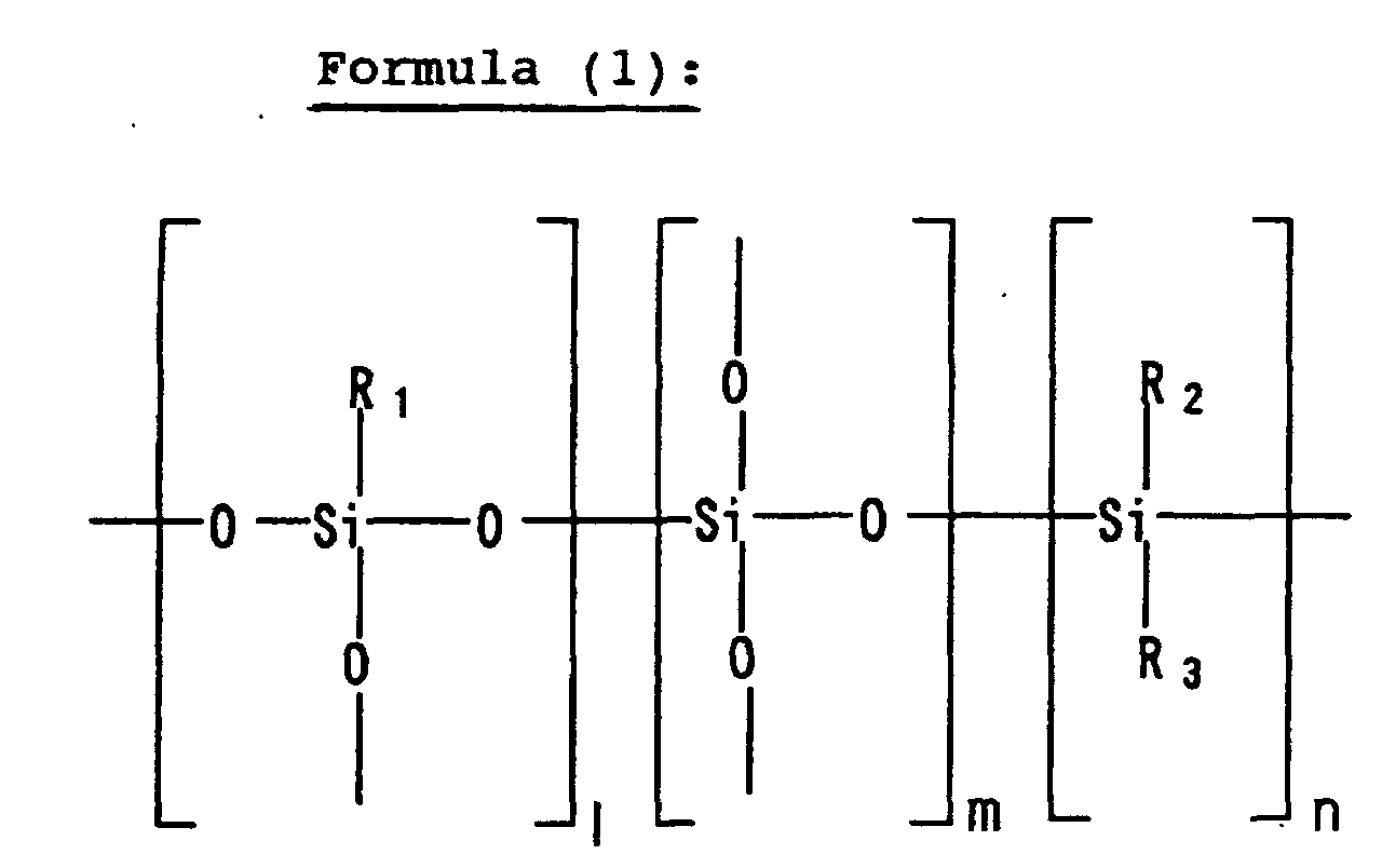
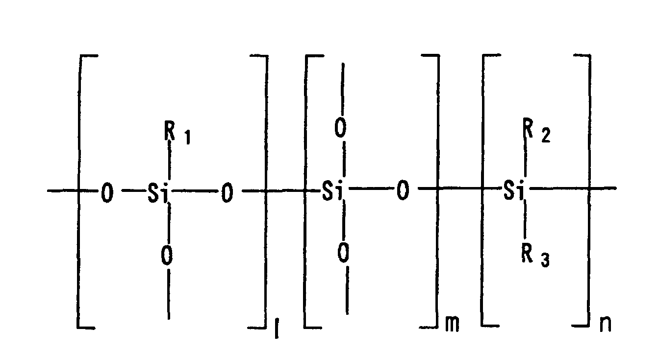
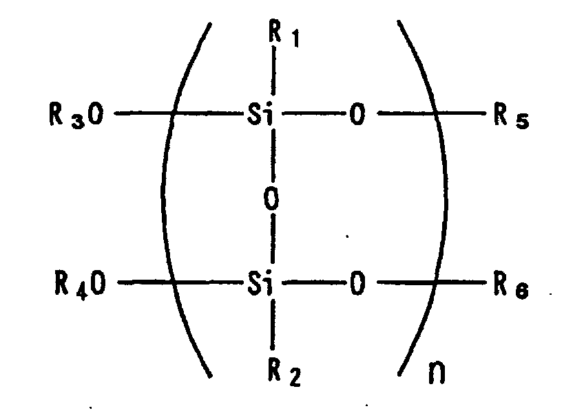
- the use of a silicone polymer represented by the general formula (1) or a silicone polymer represented by the general formula (2) is appropriate and each of them may be a mixture.
- the silicone polymer of the general formula (2) having a ladder-type structure has a rigid structure as compared with the silicone polymer of the general formula (1) whereby it has an excellent heat resistance after curing, has low stress upon forming the film and has higher withstand voltage.
- R 1 , R 2 and R 3 may be either same or different and each is an aryl group, hydrogen atom, an aliphatic alkyl group, hydroxyl group, a trialkylsilyl group or a functional group having an unsaturated bond; and 1, m and n are integers and at least 0 whereby the weight-average molecular weight is 1,000 or more)
- R 1 and R 2 may be same or different and each is an aryl group, hydrogen atom, an aliphatic alkyl group or a functional group having an unsaturated bond
- R 3 , R 4 , R 5 and R 6 may be same or different and each is hydrogen atom, an aryl group, an aliphatic alkyl group, a trialkylsilyl group or a functional group having an unsaturated bond; and
- the silicone polymer includes that which is cured upon crosslinking by light such as ultraviolet ray and its appropriate examples include that of the above formula (1) where 1% or more of the substituents R 1 , R 2 and R 3 is a functional group having an unsaturated bond and that of the above formula (2) where 1% or more of the substituents R 1 , R 2 , R 3 , R 4 , R 5 and R 6 is a functional group having an unsaturated bond.
- the functional group having an unsaturated bond is a reactive group for briding polymer molecules by crosslinking reaction or radical reaction, although an alkenyl group, an alkylacryloyl group, an alkylmethacryloyl group or styryl group is preferred, the said functional group is not limited thereto.
- the functional groups having an unsaturated bond may be introduced by a single thereof or may be introduced as a mixture of two kinds or more thereof.
- Silicone polymer having such a photocrosslinking performance is advantageous in fabricating a sensor element in view of capable of progressing curing reaction at low temperature with light as driving force by itself or by combining with a photocrosslinking agent, a photoinitiator or a photosensitizer and capable of reducing temperature applied to the control circuit or the like formed beneath the resin film or capable of carrying out self-patterning without using resist.
- the silicone resin film according to the present invention can be formed by coating a solution of silicone polymer shown by the general formula (1) and/or general formula (2), so-to-speak varnish and heating and curing thereof.
- a solution of such silicone polymer a solvent solution of an alcohol type, a ketone type, an ether type, a halogen type, an ester type, a benzene type, an alkoxybenzene type or a cyclic ketone type is appropriate.
- Silane coupling agent for improving the adhesion with surface of the sensing portion polymerizable monomer for improving the density of cured film or polymerization initiator, crosslinking agent, sensitizer or polymerization inhibitor for improving the stability upon preservation or the like may be added to the solution of the silicone polymer.
- silicone polymer having photocrosslinking performance there may be added photosensitive crosslinking agent, photopolymerization initiator, photosensitizer or the like as mentioned above.
- Photosensitive crosslinking agent and photopolymerization initiator are additives for inducing the curing of film by a radical reaction or a crosslinking reaction and as a photosensitive crosslinking agent, there are pointed out photosensitive compounds forming radical active species by light irradiation such as aromatic azide compounds, aromatic bisazide compounds, iminoquinonediazide compounds, aromatic diazo compounds, organic halogen compounds or the like, as a photopolymerization initiator, there are pointed out carbonyl compounds, dicarbonyl compounds, acetophenone, benzoin ether, acyl phosphineoxide, thioxanthone, aminocarbonyl compounds, nitrogen-containing compounds or the like.
- the silicone polymer shown by the general formula (2) containing such additives is described in the Japanese Patent Laid-Open No.Hei.10-319597 and such a polymer may be used.
- the temperature for curing treatment may vary depending upon the type of polymer, heat resistant temperature of the sensing portion or heat resistant temperature of the sensor element itself before forming the protective film or the like, it is usually suitable to be from 100°C to 400°C and, especially when the above-mentioned photocrosslinking polymer is used, the curing treatment can be carried out at a relatively low temperature of from 100°C to 250°C.
- the resin film which is formed under the sensing portion of the sensor element of the present invention is characterized in that it is a cured film of a polymer having a weight-average molecular weight of not more than 100,000 among the above-mentioned polymers.
- Resin having a low weight-average molecular weight has a melting point and, therefore, when it is subjected to a heat treatment at the temperature near the melting point, a high fluidity (reflow property) is available.
- the polymer film is fused and flows showing an improvement in stopgap property to the difference in level on the substrate whereby it is possible to make the lower layer surface of the sensing portion in a more flat state.
- any weight-average molecular weight may be acceptable although polymers having not more than 100,000 of it is preferred since they show a high reflow property.
- the flatness can be further improved especially when both of an ultrahigh-molecular polymer having a weight-average molecular weight of more than 100,000 and a polymer having a weight-average molecular weight of not more than 100,000 as the above-mentioned two or more kinds of polymers.
- the polymer having a low weight-average molecular weight has a melting point and a high fluidity (reflow property) as mentioned above and, therefore, stopgap property to the difference in level on the substrate is improved and a more flat state can be achieved.
- the ultrahigh-molecular polymers having a high weight-average molecular weight do not have a melting point and, although their fluidity at the heat treatment is low, their coverage performance for difference in level is good whereby, although the difference in level remains, it is still possible to coat the level difference with a good coverage and further possible to make the rectangular part smooth. Accordingly, when the polymers having different properties as such are jointly used, the part having a difference in level can be made in a more flat state.
- any weight-average molecular weight will do and that having an ultrahigh molecular weight of more than 100,000 is particularly preferred since it shows a low reflow property.
- a polymer where aryl group is introduced into 20% or more of the substituents (R 1 , R 2 and R 3 ) of the side chains of the above-mentioned general formula (1) or a polymer where aryl group is introduced into 20% or more of the substituents (R 1 and R 2 ) of the side chains of the above-mentioned general formula (2) is used as an ultrahigh-molecular polymer of more than 100,000, resistance to crack is improved and formation of thick film of more than 1 ⁇ m is possible.
- the resin film comprising the two kinds of polymers having different weight-average molecular weight it is possible to improve the flatness even when any of the two is firstly formed but, since the resin film comprising a low-molecular polymer has a low resistance to crack and is difficult to form a thick film, it is preferred to carry out in such a manner that the resin film comprising high-molecular polymer is firstly formed and, after the difference in level is reduced to some extent, the resin film comprising low-molecular polymer is formed in a thickness of less than the limit for crack generation because that improves the flatness.
- Fig. 1G is a cross-sectional view illustrating an example of the magnetoresistance sensor according to the present invention.
- the control circuit 2 is usually constituted by a bipolar IC and is composed of lower wiring 2a formed on the surface side of the sensor substrate 1, lower layer insulating film 2b comprising PSG or the like, upper wiring 2c formed on the lower layer insulating film 2b and interlayer insulating film 2d comprising inorganic film (silicon nitride film, silicon oxide film, etc.) formed on such surfaces by sputtering or CVD, and the like.
- control circuit 2 there is formed a resin film 3 and, on the resin film 3, there is formed a fine wiring 6 comprising magnetic metal showing a magnetoresistance effect.
- the fine wiring 6 has a fine wiring pattern comprising a plurality of wiring patterns being adjacent each other.
- a surge resistance 7 comprising AlSi for the protection of transistor and electric source to surge current is also formed on this resin film 3.
- Fine wiring 6 and upper wiring 2c of control circuit and also surge resistance 7 and upper wiring 2c of control circuit are connected by a connecting metal 8.
- a passivation film 9 comprising inorganic film (silicon nitride film, silicon oxide film, etc.) formed by means of sputtering or CVD.
- Figs.1A-1G are cross-sectional views illustrating an example of the method for the manufacture of the magnetoresistance sensor according to the present invention.
- a control circuit 2 by a usual manufacturing process for bipolar IC (Fig.1A).
- a solvent such as an alcohol type, a ketone type,
- a positive resist 4 for i-line having a thickness of 100 nm to 20 ⁇ m is coated on the surface of the resin film 3 (Fig.1C) and ultraviolet light (i-line) is irradiated from the upside using a mask 5 having a contact hole pattern for exposing contact part of the upper wiring 2c of the control circuit 2, bonding pad (not shown) or dicing line (not shown), whereupon the positive resist 4 for i-line of the contact hole part is exposed (Fig.1D).
- the resin film 3 and the interlayer insulating film 2d are continuously removed by means of a dry etching using a reactive ion etching apparatus or an ion beam etching apparatus to give a contact hole.
- a reactive ion etching apparatus or an ion beam etching apparatus to give a contact hole.
- the etching gas used in the reactive ion etching although there is no limitation so far as it is a gas species which is able to etch the resin film 3, a mixed gas comprising CF 4 , CHF 3 , C 4 F 8 , N 2 , H 2 , Ar, O 2 , etc. may be used preferably.
- the positive resist 4 for i-line on the resin film 3 is subjected to a wet removal or a dry removal using reactive ion etching apparatus, ion beam etching apparatus, ashing apparatus, etc. and then post-baked at 100°C to 450°C using an oven or a hot plate to cure the resin film 3.
- the predetermined part is opened to give a resin film 3 where the surface is made flat is obtained (Fig.1F).
- fine wiring 6 and surge resistance 7 are formed on the resin film 3 .
- Each of the fine wiring 6 and the surge resistance 7 is connected to a contact part, etc. of the upper wiring 2c of the control circuit 2 by means of a connecting metal 8 via an opening made on the resin film 3.
- a passivation film 9 comprising silicon nitride film or the like protecting the fine wiring 6 and the surge resistance 7 is formed to give a magnetoresistance sensor (Fig.1G).
- the sensing portion of the above-mentioned magnetoresistance sensor is formed on the above-mentioned resin film 3, it is possible to prevent the deterioration of sensor characteristic or the positional shift of fine wiring 6 and surge resistance 7 and it is also possible to prevent the positional shift of the upper wiring 2c or the like on the control circuit 2. Further since this resin film 3 has a high withstand voltage, deterioration of sensor characteristic by electric field caused by the control circuit 2 can be prevented when a sensing portion is formed on the control circuit 2 and, moreover, malfunction of the control circuit 2 by electric field caused by the surge resistance 7 can be prevented when the surge resistance 7 is formed on the control circuit 2.
- the resin film 3 has a low residual stress and a buffer action and, therefore, stress from the encapsulation resin is buffered and positional shift of the fine wiring 6 and the surge resistance 7 can be prevented and malfunction of sensor element thereby can be prevented when the whole sensor element is encapsulated by an encapsulation resin. Further since it has a heat resistance durable to the process for the manufacture of sensor element and has an excellent resistance to environment, it is also effective as a protective film for the control circuit 2. Furthermore, abnormality in characteristic is not noted in the evaluation of the sensor characteristic by a pressure cooker test.
- the above-mentioned interlayer insulating film 2d contains many hydroxyl groups on its surface for further improvement in adhesion to the silicone resin film.
- the resin film 3 when a resin film comprising a silicone polymer of which all substituents of side chains of R 1 , R 2 and R 3 of the above general formula (1) are hydrogen atom or aliphatic alkyl group, or a silicone polymer of which all of R 1 and R 2 in the above general formula (2) are hydrogen or aliphatic alkyl group is used, flatness of the resin film 3 is improved and compatibility of the resin film 3 with the sensing portion becomes good whereby the sensor characteristic can be improved. Hydrogen atom, methyl group and ethyl group are particularly preferred.
- R 1 , R 2 and R 3 in the general formula (1) or 20% or more of R 1 and R 2 in the general formula (2) are aryl group such as phenyl group and, when a weight-average molecular weight of the silicone polymer is made 50,000 or more, crack-resistance of the thick film is improved whereby that is more preferred.
- the polymer having a weight-average molecular weight of 100,000 or less has a melting point
- the polymer film flows upon fusion (reflow) in the direction of the low difference in level when a heat treatment is carried out near the melting point (i.e., at the temperature which is not lower than a fusing temperature and is lower than a curing temperature of the thermosetting polymer) after coating the varnish whereby it is possible that the recess portion is efficiently embedded and that the surface of the lower layer forming the sensing portion is made in a more flat state.
- the polymer having a weight-average molecular weight of 1,000-10,000 has a very high reflow property, that can be preferably used.
- the coated film thickness is same as or thinner than the difference in level, there may be the case where the rectangular shape of the difference in level still remains.
- any one of same varnish, different varnishes in viscosity and varnishes constituted by different polymer may be used.
- a resin film comprising a polymer with high reflow and good filling-in properties having a low weight-average molecular weight is formed whereupon, although the rectangular shape of the difference in level still remains, the difference in level can be filled in by the resin film to some extent.
- a resin film comprising a polymer with a good coverage performance for difference in level having a high weight-average molecular weight is layered on this surface, the rectangular shape can be made smooth and the residual difference in level is filled up whereupon the more flat state can be resulted.
- the order of formation of a resin film comprising a polymer having a low weight-average molecular weight and another resin film comprising a polymer having a high weight-average molecular weight may be free but, since the resin film comprising a low weight-average molecular weight has low resistance to crack and is difficult to form a thick film, the flatness is more improved when the resin film comprising a polymer having a high weight-average molecular weight is firstly formed to more or less reduce the difference in level and then the resin film comprising a low weight-average molecular weight is used to form a film thickness of not more than the limit for generation of crack.
- sensor element although there is no particular limitation so far as it is a sensor, there is particularly used magnetoresistance sensor, air flow sensor, acceleration sensor, pressure sensor, yaw rate sensor or image sensor as sensor element.
- a resin film is formed on the sensor substrate where an insulating film is formed on the surface or that the resin film is directly formed on the sensor substrate comprising glass substrate or silicon substrate. In that case, a sensing portion is formed on that resin film as well.
- the sensing portion (fine wiring 6) in the above sensor element, although depending on a kind of the sensor, there may be used metal such as Au, Al, Ag, Bi, Ce, Cr, Cu, Co, C, Fe, Hf, In, Mo, Mg, Ni, Nb, Pb, Pt, Si, Sn, Ti, Ta, V, W, Zn, Zr or the like and alloy, oxide, nitride, silicide, sulfide, carbide, fluoride or the like comprising the metals.
- metal such as Au, Al, Ag, Bi, Ce, Cr, Cu, Co, C, Fe, Hf, In, Mo, Mg, Ni, Nb, Pb, Pt, Si, Sn, Ti, Ta, V, W, Zn, Zr or the like and alloy, oxide, nitride, silicide, sulfide, carbide, fluoride or the like comprising the metals.
- alloy such as Al-Cu, Al-Si, Cu-Cr, Cu-Ni, Ni-Cr, Ni-Fe, Al-Si-Cu, Ni-Cr-Si, Al-Sc, Co-Cr or the like, oxide such as Al 2 O 3 , CeO 2 , CuO, Fe 2 O 3 , HfO 2 , MgO, Nb 2 O 5 , SiO, SiO 2 , TiO, TiO 2 , Ta 2 O 5 , ZrO 2 or the like, nitride such as AlN, Cr 2 N, Si 3 N 4 , TiN, ZrN or the like, silicide such as CrSi 2 , MoSi 2.5 , WSi 2 , WSi 0.4 or the like, sulfide such as ZnS, carbide such as SiC, TiC, WC or the like and fluoride such as MgF 2 or the like.
- oxide such as Al 2 O 3 , CeO 2 , CuO, Fe 2 O
- the positive resist 4 for i-line is used but, so far as a desired pattern formation can be formed, any of positive resist and negative resist may be used and, moreover, any of that for g ray, i-line, KrF excimer and ArF excimer may be used.
- ultraviolet ray is irradiated on whole area of the pattern of the positive resist 4 for i-line to increase the crosslinking density whereby the resistance of the developer or rinsing solution exclusively for the said resin film is enhanced.
- the resin film 3 is removed by a developing treatment and the interlayer insulating film 2d is removed by a dry etching.
- the developing treatment is carried out in such a manner that a dipping development or a spin development is conducted using the developing solution exclusively for the resin film followed by washing using a rinse solution exclusively for the resin film.
- oxidation of the surface layer of the resin film 3 can be lowered when it is conducted under the condition of low pressure and low power. Especially under the low pressure condition of not more than 1 Torr and the low power condition of not more than 1 kW, oxidation of the surface of the resin film 3 can be further lowered.
- a resin film 3 is formed on the control circuit 2 where an interlayer insulating film 2d is formed on the surface and is functioned especially as a stress buffering film and a flattening film
- the resin film 3 comprising such a polymer is directly formed on the control circuit 2 where no interlayer insulating film 2d is formed on the surface so that it functions as a protective film as well in addition to the functions as stress buffering film and flattening film.
- the resin film 3 is formed by a rotary coating and, therefore, it is possible for the resin film 3 to avoid the damage by radioactive ray of the control circuit 2 caused by plasma irradiation.
- the interlayer insulating film 2d includes a large amount of hydroxyl groups at its surface to further improve the adhesion to the resin film 3.
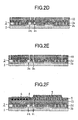
- Fig.2F is a cross-sectional view for illustrating another example of the magnetoresistance sensor according to the present invention.
- the magnetoresistance sensor there is an photocured resin film 13 between the sensor substrate 1 where the control circuit 2 is formed on the surface and the sensing portion constituted by fine wiring 6.
- Other constitutions are the same as those in Fig.1.
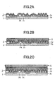
- Figs.2A-2F are cross-sectional views illustrating another example of the method of fabricating the magnetoresistance sensor according to the present invention.
- the method of fabricating the magnetoresistance sensor differs from the above-described method in that there is used a compound prepared by dissolving polymer having photocrosslinking performance in a solvent and adding a photocrosslinking agent or photopolymerization agent thereto.
- a polyimide polymer, a silicone polymer or the like may be used for the polymer having photocrosslinking performance.
- a method for the formation of pattern of resin film comprising silicone polymer is described, for example, in the Japanese Patent Laid-Open No.Hei.10-319597.
- a varnish of a polymer having photocrosslinking performance is coated, by the same manner as above, on a sensor substrate 1 where the control circuit 2 is formed on its surface and subjected to a heat treatment at 100°C to 250°C (Fig.2A and Fig.2B). Then, irradiation and exposure to light are carried out from upside using a mask 15 having a desired pattern and the area of the resin film where no light is irradiated is removed by means of a developing treatment and post-baked at 100°C to 450°C to cure the resin film. As a result, there is prepared a flat resin film 13 where the predetermined area is opened (Fig.2C and Fig.2D).
- Photosensitive crosslinking agent and photopolymerization initiator are usually added to induce the reaction using light as a driving force and are decomposed by heat treatment as well to thereby cause curing reaction.
- the polymer is formed on the sensor element and therefor, a temperature condition of curing thereof directly effects adverse influence on the sensor characteristic, however, the polymer having high molecular weight is provided with heat resistance at 500°C even when the polymer is not thermally cured, by adding the additives, curing temperature in forming the film can be lowered and the polymer can be baked at temperature equal to or lower than heat resistance limit temperature of the sensor element.
- the additives by adding the additives, photosensitivity is manifested, when a pattern needs to transcribe on the resin film, by irradiating ultraviolet ray directly to the resin film via a mask having a desired pattern and developing thereof, the pattern can be formed. Therefore, the resist pattern forming step can be dispensed with, the pattern can be transcribed in a short period of time and stably, the additives can contribute to simplification of the process and reduction of the cost.
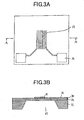
- Figs.3A-3B are drawings which illustrate the structure of air flow sensor of Example 1 according to the present invention where Fig.3A is a plane view and Fig.3B is a cross-sectional view along the line A-A in FiG.3A.
- the air flow sensor there is a resin film 34 between a silicon substrate 31 where the lower supporting film 32 is formed on its surface and a sensing portion constituted by a metal wire 33 comprising microfine wiring pattern in a zigzag shape. Bonding pads 35 for detecting a change in an electric resistance value is provided to connect to both ends of the metal wire 33.
- An upper supporting film 36 is formed on the surfaces of the metal wire 33 and the resin film 34.
- a recess portion 37 is provided below the sensing portion of the silicon substrate 31.
- the air flow sensor detects a flow rate of a gas by detecting a heat amount of the metal wire 33 which is conducted and heated and which is deprived by depending upon the flow rate of the gas passing through the recess portion 37 by a change in the electric resistance value.
- a lower supporting film 32 comprising silicon nitride film formed by a sputtering apparatus on the front face side of a silicon substrate 31 having a thickness of about 300 ⁇ m.
- a varnish (PIX-1400; manufactured by Hitachi Chemical) of a polyimide polymer dissolved in an organic solvent such as N-methylpyrrolidone, etc. was rotationally coated at the rate of 3,000 rpm onto the surface of the lower supporting film 32 comprising silicon nitride film and dried by a heat treatment on a hot plate at 120°C for 1 minute to thereby carry out a surface treatment. Further, postbaking was carried out in an oven at 350°C for 1 hour to thereby completely cure the varnish to thereby form a polyimide resin film 34 having a film thickness of about 2 ⁇ m.
- the positive resist for i-line was rotationally coated on the polyimide resin film 34 to make the film thickness about 5 ⁇ m and normal photolithography was carried out to thereby provide a positive resist pattern for i-line for opening desired dicing lines.
- the dry etching was carried out by using a reactive ion etching apparatus and using a gas having a mixture ratio of C 4 F 8 /O 2 of 3/7 as the gas for dry etching. Further, the positive resist for i-line was ashed to remove by an oxygen plasma to thereby provide a polyimide resin film 34 a predetermined portion of which was opened.
- metal wire 33 comprising Pt which is to be a temperature sensor
- bonding pads 35 and upper supporting film 36 comprising silicon nitride film were formed in this order on the polyimide resin film 34.
- the silicon substrate 31 right below the metal wire 33 was removed by a wet etching to form a recess portion 37.
- the bonding pads 35 and a lead frame were connected by a bonding wire (not shown).
- the metal wire 33 comprising Pt which is conducted with electricity is heated at the temperature higher than the outer air temperature by about 100°C and the metal wire 33 comprising Pt is deprived of heat and temperature thereof is lowered by depending upon flow intensity of gas flow. Since the resistance value of the metal wire 33 comprising Pt changes depending upon temperature thereof, the deprived heat amount can electrically be detected. Since the deprived heat amount and the flow intensity of the gas flow correspond to each other in a one-to-one relationship, the flow of gas can be known.
- Fig.1G is a cross-sectional view illustrating the structure of a magnetoresistance sensor of Example 2 according to the present invention. Formation of a silicone resin film as a resin film 3 on the surface of an interlayer insulating film 2d of control circuit 2 constituted by bi-polar IC was carried out by the following method.
- the varnish (b) was rotationally coated at the rate of 2,500 rpm on the surface of the interlayer insulating film 2d and cured by subjecting to a heat treatment at 250°C for 5 minutes on a hot plate.
- a silicone resin film having a film thickness of 1.3 ⁇ m was formed. Although the coverage performance for difference in level was good, a sufficient flattening was not achieved but difference of 1.2 ⁇ m in level still remained.
- the varnish (a) was rotationally coated at the rate of 2,500 rpm on the surface of the silicone resin film and subjected to a heat treatment on a hot plate at the temperature of from 120°C to 200°C which was near the melting point of the silicone polymer whereupon the silicone polymer was reflowed.
- the silicone polymer flowed to the part having a difference in level whereby the difference in level was able to be almost nil.
- a positive resist for i-line was rotationally coated on the surface thereof to constitute the film thickness about 5 ⁇ m and a normal photolithography was carried out to thereby provide a resist layer having a desired pattern such as contact hole, dicing line or the like.
- a reactive ion etching or an ion beam etching may be preferably used.
- the dry etching was carried out by using a reactive ion etching and using a gas having a mixture ratio of CF 4 /O 2 of 8/2 as the gas for the dry etching.
- the positive resist 4 for i-line was ashed to remove by oxygen plasma to thereby complete the patterning of the resin film 3.
- a surge resistance 7 comprising AlSi and fine wiring 6 of magnetic metal showing a magnetoresistance effect and a connecting metal 8 connecting the contact part of the upper layer wiring 2c of control circuit 2 to surge resistance 6 and fine wiring 5.
- a passivation film 9 comprising silicone nitride film or the like for protecting the surge resistance 7 and the fine wiring 6.
- Fig.2F is a cross-sectional view illustrating the structure of the magnetoresistance sensor of Example 3 according to the present invention. Formation of multiple layers of silicone resin film and photocured silicone resin film as resin films 13 on the surface of interlayer insulating film 2d of control circuit 2 constituted by bipolar IC was carried out as follows.
- the aqueous solution (c) for reinforcing a close adhesion was rotationally coated at the rate of 2,000 rpm on the substrate in which a control circuit having a maximum difference in level of 2.5 ⁇ m was formed. It is subjected to a heat treatment on a hot plate at 110°C for 2 minutes. After that, the varnish (a) was rotationally coated thereon at the rate of 2,000 rpm, subjected to a heat treatment on a hot plate for 5 minutes at 120°C near the melting point of this silicone polymer to reflow the resin film and post-baked at 375°C for 1 hour in an oven to form the first layer of a silicone resin film having a thickness of 1.2 ⁇ m.
- the varnish (b) was rotationally coated thereon at the rate of 3,000 rpm to make the film thickness about 3 ⁇ m and subjected to a heat treatment on a hot plate at 135°C to form the second layer of the silicone resin film.
- the difference in level became 10% or less of the initial stage.
- This was further subjected to a contact exposure to ultraviolet ray from an ultrahigh pressure mercury lamp at the output of 500 mJ/cm 2 by passing through a photomask having the desired pattern such as contact hole and dicing line.
- the first layer of the silicone resin film and the interlayer insulating film were continuously removed by a dry etching using the pattern of the silicone resin film as a mask.
- the dry etching method there is no limitation for the dry etching method so far as it is a method which dose not affect the silicone resin film, reactive ion etching or ion beam etching may be preferably used.
- the dry etching was carried out by using a reactive ion etching and using a gas having a mixture ratio of CF 4 /O 2 /Ar of 5/3/2 as the gas for the dry etching. As such, the pattern formation of the resin film having a two-layered structure was completed.
- Example 3 Sensor characteristic and durability of the magnetoresistance sensor element were tested and there were obtained the sensor characteristic and the durability which were same as or better than those formed on a flat substrate.
- Example 3 the same effect as in Example 2 is achieved and a step of formation of resist pattern can be eliminated whereupon that is able to contribute to simplification of the process and to making the cost low. Since a process can be skipped, it can contribute to simplification of a process and reduction of cost.
- the sensor element according to the present invention is suitable for achieving the improvement in reliability of sensor element and is suitable to be used as, for example, a magnetoresistance sensor, an air flow sensor, an acceleration sensor, a pressure sensor, a yaw rate sensor and an image sensor.
Landscapes
- Physics & Mathematics (AREA)
- General Physics & Mathematics (AREA)
- Fluid Mechanics (AREA)
- Condensed Matter Physics & Semiconductors (AREA)
- Hall/Mr Elements (AREA)
- Formation Of Insulating Films (AREA)
- Measuring Magnetic Variables (AREA)
- Measuring Volume Flow (AREA)
- Testing Or Calibration Of Command Recording Devices (AREA)
- Silicon Polymers (AREA)
- Pressure Sensors (AREA)
Abstract
Description

Since a process can be skipped, it can contribute to simplification of a process and reduction of cost.
Claims (14)
- A sensor element comprising;
a sensor substrate; and
a sensing portion supported by the sensor substrate;
wherein a resin film is provided between the sensor substrate and the sensing portion. - The sensor element according to claim 1, wherein the sensing portion has a microfine wiring pattern.
- The sensor element according to claim 2, wherein the microfine wiring pattern comprises plural wiring patterns being adjacent each other.
- The sensor element according to claim 1, wherein the resin film is a cured film of a curing polymer selected from a silicone polymer, a polyimide polymer, a polyimide silicone polymer, a polyarylene ether polymer, a bisbenzocyclobutene polymer, a polyquinoline, a perfluorohydrocarbon, a fluorocarbon polymer and an aromatic hydrocarbon polymer.
- The sensor element according to claim 4, wherein the curing polymer is a photo-curing polymer.
- The sensor element according to claim 1, wherein the resin film is a cured film of the silicone polymer represented by the general formula (1);wherein R1, R2 and R3, which may be the same or different, each is an aryl group, hydrogen atom, an aliphatic alkyl group, hydroxyl group, a trialkylsilyl group or a functional group having an unsaturated bond; and 1, m and n are integers and at least 0; has a weight-average molecular weight of not less than 1,000.
- The sensor element according to claim 1, wherein the resin film is a cured film of the silicone polymer represented by the general formula (2);wherein R1 and R2, which may be same or different, each is an aryl group, hydrogen atom, an aliphatic alkyl group or a functional group having an unsaturated bond; R3, R4, R5 and R6, which may be same or different, each is hydrogen atom, an aryl group, an aliphatic alkyl group, a trialkylsilyl group or a functional group having an unsaturated bond; and n is an integer; and has a weight-average molecular weight of not less than 1,000.
- The sensor element according to claim 4, wherein the resin film comprises layered film comprising plural layers and each of the layers comprises cured film of different curing polymer.
- The sensor element according to claim 8, wherein each of the layered film comprises a cured film of curing polymer having different molecular weight.
- The sensor element according to claim 9, wherein the layered film is composed of a cured film comprising a silicone polymer having a weight-average molecular weight of not less than 100,000 and a cured film comprising a silicone polymer having a weight-average molecular weight of not more than 100,000.
- The sensor element according to claim 8, wherein the uppermost layer of the layered film comprising plural layers comprises a cured film of a photo-curing polymer.
- The sensor element according to claim 1, wherein the sensor element is selected from a magnetoresistance sensor, an air flow sensor, an acceleration sensor, a pressure sensor, a yaw rate sensor or an image sensor.
- A method of fabricating a sensor element, comprising a step of coating a solution of a thermosetting polymer on a sensor substrate to form a curing polymer film, a step of heating the curing polymer film at temperatures which are not lower than a fusing temperature and are lower than a curing temperature of the thermosetting polymer, a step of heating thereof at the temperature of not lower than the curing temperature to form a cured resin film and a step of forming a desired sensing portion on the cured resin film.
- The method of fabricating a sensor element according to claim 13, wherein the thermosetting polymer is selected from a silicone polymer, a polyimide polymer, a polyimide silicone polymer, a polyarylene ether polymer, a bisbenzocyclobutene polymer, a polyquinoline polymer, a perfluorohydrocarbon polymer, a fluorocarbon polymer or an aromatic hydrocarbon polymer.
Applications Claiming Priority (1)
| Application Number | Priority Date | Filing Date | Title |
|---|---|---|---|
| PCT/JP2000/003077 WO2001088482A1 (en) | 2000-05-15 | 2000-05-15 | Sensor element and its manufacturing method |
Publications (2)
| Publication Number | Publication Date |
|---|---|
| EP1284412A1 true EP1284412A1 (en) | 2003-02-19 |
| EP1284412A4 EP1284412A4 (en) | 2006-10-25 |
Family
ID=11736022
Family Applications (1)
| Application Number | Title | Priority Date | Filing Date |
|---|---|---|---|
| EP00927757A Withdrawn EP1284412A4 (en) | 2000-05-15 | 2000-05-15 | DETECTION ELEMENT AND METHOD OF MANUFACTURING |
Country Status (5)
| Country | Link |
|---|---|
| US (1) | US6732583B1 (en) |
| EP (1) | EP1284412A4 (en) |
| JP (1) | JP3941505B2 (en) |
| KR (1) | KR100683321B1 (en) |
| WO (1) | WO2001088482A1 (en) |
Cited By (1)
| Publication number | Priority date | Publication date | Assignee | Title |
|---|---|---|---|---|
| WO2007034240A3 (en) * | 2005-09-20 | 2007-11-29 | Bae Systems Plc | Sensor device with backside contacts |
Families Citing this family (13)
| Publication number | Priority date | Publication date | Assignee | Title |
|---|---|---|---|---|
| US7258003B2 (en) | 1998-12-07 | 2007-08-21 | Honeywell International Inc. | Flow sensor with self-aligned flow channel |
| KR100633655B1 (en) | 1999-12-22 | 2006-10-11 | 미쓰비시덴키 가부시키가이샤 | Sensor element and its manufacturing method |
| ATE278956T1 (en) * | 2000-07-27 | 2004-10-15 | Micronas Holding Gmbh | SENSOR CHIPS WITH POLYSILOXANE MULTIPLE LAYERS |
| JP3713008B2 (en) * | 2002-09-30 | 2005-11-02 | 長野計器株式会社 | Method for manufacturing strain amount detection device |
| KR100590211B1 (en) * | 2002-11-21 | 2006-06-15 | 가부시키가이샤 덴소 | Magnetic impedance device, sensor apparatus using the same and method for manufacturing the same |
| US7461559B2 (en) * | 2005-03-18 | 2008-12-09 | Citizen Holdings Co., Ltd. | Electromechanical transducer and method of fabricating the same |
| US20070209433A1 (en) * | 2006-03-10 | 2007-09-13 | Honeywell International Inc. | Thermal mass gas flow sensor and method of forming same |
| WO2008026328A1 (en) * | 2006-08-30 | 2008-03-06 | Alps Electric Co., Ltd. | Magnetism detector and its manufacturing method |
| JP4485499B2 (en) * | 2006-09-04 | 2010-06-23 | アルプス電気株式会社 | Magnetic detection device and manufacturing method thereof |
| WO2009031539A1 (en) * | 2007-09-03 | 2009-03-12 | Alps Electric Co., Ltd. | Magnetic detecting device |
| US20130020117A1 (en) * | 2009-12-14 | 2013-01-24 | Daicel Corporation | Laminated body comprising porous layer and functional laminate using same |
| US8804344B2 (en) * | 2011-06-10 | 2014-08-12 | Scott Moncrieff | Injection molded control panel with in-molded decorated plastic film |
| US10533963B2 (en) * | 2017-01-09 | 2020-01-14 | Mobiosense Corp. | Biosensor device |
Family Cites Families (11)
| Publication number | Priority date | Publication date | Assignee | Title |
|---|---|---|---|---|
| US5056362A (en) * | 1990-07-25 | 1991-10-15 | Siemens Automotive L.P. | Strengthening a silicon micromachined mass air flow sensor in the region of its hot element |
| JPH05121793A (en) | 1991-10-24 | 1993-05-18 | Nec Corp | Method of manufacturing magnetoresistive element |
| JP3085100B2 (en) * | 1994-09-07 | 2000-09-04 | 株式会社村田製作所 | Magnetoelectric conversion element |
| JPH08178768A (en) * | 1994-12-20 | 1996-07-12 | Matsushita Electric Ind Co Ltd | Mechanical quantity sensor |
| US5631417A (en) * | 1995-09-06 | 1997-05-20 | General Motors Corporation | Mass air flow sensor structure with bi-directional airflow incident on a sensing device at an angle |
| US5789020A (en) * | 1996-03-11 | 1998-08-04 | The United States Of America As Represented By The Administrator Of The National Aeronautics And Space Administration | Method of forming a hot film sensor system on a model |
| JPH09304127A (en) * | 1996-05-17 | 1997-11-28 | Tdk Corp | Multifunctional sensor component |
| US6448624B1 (en) * | 1996-08-09 | 2002-09-10 | Denso Corporation | Semiconductor acceleration sensor |
| JPH10239264A (en) * | 1997-02-25 | 1998-09-11 | Sanriki Kogyo Kk | Electric resistance type moisture sensor |
| JPH10319597A (en) * | 1997-05-23 | 1998-12-04 | Mitsubishi Electric Corp | Photosensitive silicone ladder resin composition, pattern transfer method for transferring a pattern to the resin composition, and semiconductor device using the above resin composition |
| JP3544141B2 (en) * | 1998-05-13 | 2004-07-21 | 三菱電機株式会社 | Magnetic detecting element and magnetic detecting device |
-
2000
- 2000-05-15 JP JP2001584831A patent/JP3941505B2/en not_active Expired - Fee Related
- 2000-05-15 KR KR1020027000540A patent/KR100683321B1/en not_active Expired - Fee Related
- 2000-05-15 EP EP00927757A patent/EP1284412A4/en not_active Withdrawn
- 2000-05-15 WO PCT/JP2000/003077 patent/WO2001088482A1/en not_active Ceased
- 2000-05-15 US US10/030,426 patent/US6732583B1/en not_active Expired - Lifetime
Cited By (2)
| Publication number | Priority date | Publication date | Assignee | Title |
|---|---|---|---|---|
| WO2007034240A3 (en) * | 2005-09-20 | 2007-11-29 | Bae Systems Plc | Sensor device with backside contacts |
| US8143689B2 (en) | 2005-09-20 | 2012-03-27 | Bae Systems Plc | Sensor device |
Also Published As
| Publication number | Publication date |
|---|---|
| KR20020019523A (en) | 2002-03-12 |
| JP3941505B2 (en) | 2007-07-04 |
| US6732583B1 (en) | 2004-05-11 |
| WO2001088482A1 (en) | 2001-11-22 |
| EP1284412A4 (en) | 2006-10-25 |
| KR100683321B1 (en) | 2007-02-15 |
Similar Documents
| Publication | Publication Date | Title |
|---|---|---|
| KR100633655B1 (en) | Sensor element and its manufacturing method | |
| US6732583B1 (en) | Sensor element and its manufacturing method | |
| EP0501178B1 (en) | Bilayer metallization cap for photolithography | |
| JPWO2001046708A1 (en) | Sensor element and manufacturing method thereof | |
| EP0130338B1 (en) | Resist structure and processes for making and patterning it | |
| EP0230615A2 (en) | Silicon-containing polyimides as oxygen etch stop and dual dielectric coatings | |
| JPH1160735A (en) | Polysilane and pattern forming method | |
| JPH0627671A (en) | Photosensitive silicon-contained resist composition and its usage method | |
| JPH0456977B2 (en) | ||
| JPWO2001088482A1 (en) | Sensor element and manufacturing method thereof | |
| WO2001067180A1 (en) | Method for forming resist pattern in reverse-tapered shape | |
| JPH05190684A (en) | Semiconductor device and manufacture thereof | |
| US20230197505A1 (en) | Method for Patterning a Substrate Using Photolithography | |
| JP4852360B2 (en) | Method for forming a base layer composition, lithographic structure, material layer or material element comprising a heterocyclic aromatic structure used in a multilayer lithography process on a substrate | |
| JP4423119B2 (en) | Antireflection film and optical element using the same | |
| CN103460135B (en) | For device fabrication can exposure image and the silsesquioxane resins that can develop | |
| JP2005183472A (en) | Magnetoresistive sensor element | |
| JPH06314727A (en) | Photolithography test structure and integrated circuit photolithography test structure | |
| US6004730A (en) | Method of forming an insulating film pattern and photosensitive composition | |
| EP1057642B1 (en) | Method of manufacturing a liquid discharge head, liquid discharge head manufactured by the same method, and method of manufacturing a minute mechanical apparatus | |
| JPS6243544B2 (en) | ||
| JP2002170883A (en) | Method for fabricating wiring structure for semiconductor device | |
| JP2002270690A (en) | Wiring structure of semiconductor device | |
| JP2000100699A (en) | Pattern formation method | |
| JP2954442B2 (en) | Wiring pattern forming method |
Legal Events
| Date | Code | Title | Description |
|---|---|---|---|
| PUAI | Public reference made under article 153(3) epc to a published international application that has entered the european phase |
Free format text: ORIGINAL CODE: 0009012 |
|
| 17P | Request for examination filed |
Effective date: 20020121 |
|
| AK | Designated contracting states |
Designated state(s): AT BE CH CY DE DK ES FI FR GB GR IE IT LI LU MC NL PT SE |
|
| RBV | Designated contracting states (corrected) |
Designated state(s): DE FR |
|
| RAP1 | Party data changed (applicant data changed or rights of an application transferred) |
Owner name: MITSUBISHI DENKI KABUSHIKI KAISHA |
|
| A4 | Supplementary search report drawn up and despatched |
Effective date: 20060927 |
|
| 17Q | First examination report despatched |
Effective date: 20081203 |
|
| GRAP | Despatch of communication of intention to grant a patent |
Free format text: ORIGINAL CODE: EPIDOSNIGR1 |
|
| RIC1 | Information provided on ipc code assigned before grant |
Ipc: G01R 33/09 20060101ALI20170828BHEP Ipc: G01F 1/684 20060101AFI20170828BHEP |
|
| INTG | Intention to grant announced |
Effective date: 20170927 |
|
| STAA | Information on the status of an ep patent application or granted ep patent |
Free format text: STATUS: THE APPLICATION HAS BEEN WITHDRAWN |
|
| 18W | Application withdrawn |
Effective date: 20171211 |