EP1284311A2 - Silicon semiconductor substrate and process for producing the same - Google Patents
Silicon semiconductor substrate and process for producing the same Download PDFInfo
- Publication number
- EP1284311A2 EP1284311A2 EP02017733A EP02017733A EP1284311A2 EP 1284311 A2 EP1284311 A2 EP 1284311A2 EP 02017733 A EP02017733 A EP 02017733A EP 02017733 A EP02017733 A EP 02017733A EP 1284311 A2 EP1284311 A2 EP 1284311A2
- Authority
- EP
- European Patent Office
- Prior art keywords
- atoms
- silicon
- depth
- concentration
- oxygen
- Prior art date
- Legal status (The legal status is an assumption and is not a legal conclusion. Google has not performed a legal analysis and makes no representation as to the accuracy of the status listed.)
- Granted
Links
Classifications
-
- C—CHEMISTRY; METALLURGY
- C30—CRYSTAL GROWTH
- C30B—SINGLE-CRYSTAL GROWTH; UNIDIRECTIONAL SOLIDIFICATION OF EUTECTIC MATERIAL OR UNIDIRECTIONAL DEMIXING OF EUTECTOID MATERIAL; REFINING BY ZONE-MELTING OF MATERIAL; PRODUCTION OF A HOMOGENEOUS POLYCRYSTALLINE MATERIAL WITH DEFINED STRUCTURE; SINGLE CRYSTALS OR HOMOGENEOUS POLYCRYSTALLINE MATERIAL WITH DEFINED STRUCTURE; AFTER-TREATMENT OF SINGLE CRYSTALS OR A HOMOGENEOUS POLYCRYSTALLINE MATERIAL WITH DEFINED STRUCTURE; APPARATUS THEREFOR
- C30B29/00—Single crystals or homogeneous polycrystalline material with defined structure characterised by the material or by their shape
- C30B29/02—Elements
- C30B29/06—Silicon
-
- H—ELECTRICITY
- H10—SEMICONDUCTOR DEVICES; ELECTRIC SOLID-STATE DEVICES NOT OTHERWISE PROVIDED FOR
- H10P—GENERIC PROCESSES OR APPARATUS FOR THE MANUFACTURE OR TREATMENT OF DEVICES COVERED BY CLASS H10
- H10P95/00—Generic processes or apparatus for manufacture or treatments not covered by the other groups of this subclass
- H10P95/90—Thermal treatments, e.g. annealing or sintering
-
- C—CHEMISTRY; METALLURGY
- C30—CRYSTAL GROWTH
- C30B—SINGLE-CRYSTAL GROWTH; UNIDIRECTIONAL SOLIDIFICATION OF EUTECTIC MATERIAL OR UNIDIRECTIONAL DEMIXING OF EUTECTOID MATERIAL; REFINING BY ZONE-MELTING OF MATERIAL; PRODUCTION OF A HOMOGENEOUS POLYCRYSTALLINE MATERIAL WITH DEFINED STRUCTURE; SINGLE CRYSTALS OR HOMOGENEOUS POLYCRYSTALLINE MATERIAL WITH DEFINED STRUCTURE; AFTER-TREATMENT OF SINGLE CRYSTALS OR A HOMOGENEOUS POLYCRYSTALLINE MATERIAL WITH DEFINED STRUCTURE; APPARATUS THEREFOR
- C30B33/00—After-treatment of single crystals or homogeneous polycrystalline material with defined structure
-
- H—ELECTRICITY
- H10—SEMICONDUCTOR DEVICES; ELECTRIC SOLID-STATE DEVICES NOT OTHERWISE PROVIDED FOR
- H10P—GENERIC PROCESSES OR APPARATUS FOR THE MANUFACTURE OR TREATMENT OF DEVICES COVERED BY CLASS H10
- H10P36/00—Gettering within semiconductor bodies
- H10P36/20—Intrinsic gettering, i.e. thermally inducing defects by using oxygen present in the silicon body
Definitions
- the present invention relates to a silicon semiconductor substrate obtained, by slicing, from a silicon single crystal which has been produced by pulling up the silicon single crystal by Czochralski method (CZ method) or magnetic field-applied Czochralski method (MCZ method) while controlling the cooling rate in a range from the coagulation temperature to the crystallising temperature of a single crystal and also controlling the concentration of nitrogen, the concentration of oxygen and the like.
- CZ method Czochralski method
- MCZ method magnetic field-applied Czochralski method
- the invention also relates to a process for producing the same.
- ring stacking faults As for the Grow-in defects during the growth of a silicon single crystal causing the reduction in the yield of a device, ring stacking faults (R-SF), dislocation clusters and the like occur in a zone where interstitial silicon is dominant, and cavity defects, namely void type defects (COP, LSTD, FPD) and AOP occur in a zone where voids are dominant.
- COP Crystal Originated Particles
- a void of about 0.1 ⁇ m in size formed on a substrate just after the substrate is produced has been attracting considerable attention.
- the substance of this defect is considered to be a void in the crystal having an octahedral shape, which is estimated to cause pattern failures and structural destruction of the device.
- quartz is used as the crucible.
- Oxygen eluted from the quartz crucible while pulling up a single crystal is moved by the flow and diffusion of the silicon melt and a large part of oxygen is evaporated as SiO gas from the surface of the melt.
- a part of the oxygen is incorporated into the crystal at high temperature, and the content of oxygen is supersaturated in the course of cooling the crystal, forming, in the crystal, micro-defects (BMD) of oxygen precipitates with a diameter of several hundreds nm or less and consisting of SiO 2 or SiO x .
- the micro-defects of oxygen precipitates become extinct on the surface layer portion of the semiconductor substrate which is the active area of the electronic device and it is possible to increase the density of the micro-defects (BMD) in a deep zone far apart from the substrate surface and to increase the size of the oxygen precipitates.
- BMD micro-defects
- the depth of the denuded zone and the density of the micro-defect inside a semiconductor substrate depend upon the concentration of oxygen and the concentration of nitrogen in a silicon single crystal and the cooling rate during the growth of the single crystal.
- concentration of oxygen, the concentration of nitrogen and the cooling rate have been controlled to control the silicon defect-free layer and the density of the micro-defects in the inside.
- the concentration of oxygen in the silicon single crystal wafer is 9 to 17 ppma
- a silicon single crystal bar is grown in a manner that the cooling rate in a temperature range from 1150 °C to 1080 °C during the growth of the crystal is controlled to be in a range from 1.0 to 4.5 °C/min.
- DZ denuded zone
- a denuded zone is formed only to the depth of 12 ⁇ m (evaluation by COP number) by selecting an oxygen concentration of 9 to 17 ppma when the concentration of nitrogen is in the range from 1x10 12 to 1x10 15 atoms/cm 3 , and a silicon single crystal wafer with the depth of the denuded zone larger than 12 ⁇ m could not be produced.
- the present invention is to provide a silicon semiconductor substrate in which the denuded zone (DZ) is deeper than 12 ⁇ m or the depth of the denuded zone of a void type defect is larger than 12 ⁇ m, the semiconductor substrate having a portion with locally increased nitrogen concentration which is produced by nitrogen segregation and exhibiting a signal strength two or more times the average signal strength at the depth of 12 ⁇ m or more below the surface thereof when measuring the concentration of nitrogen by secondary ion mass-spectroscopy, and having a high freedom in the production of electronic devices and a high device yield.
- the present invention is also to provide a process for producing the same.
- the depth of the denuded zone is evaluated by the depth having both values of the depth of the void type defect and the acceptable depth for withstanding voltage.
- the density of oxygen precipitates means the density of micro-defects caused by SiO 2 resulting from the precipitation of heat-treated interstitial oxygen solved as a supersaturated solid solution in a silicon single crystal and micro-defects resulting from a dislocation caused by a stacking fault along with the formation of SiO 2 .
- a silicon semiconductor wafer obtained from a silicon single crystal grown by a method selected from the group consisting of Czochralski method and a magnetic field-applied Czochralski method the silicon semiconductor wafer comprising, after heat-treatment in a non-oxidising atmosphere, a denuded zone with a depth of at least 12 ⁇ m and a crystal defect density of oxygen precipitates of at least 5x10 8 /cm 3 at a centre of a thickness of the silicon semiconductor wafer.
- the non-oxidising atmosphere may be a non-oxidising atmosphere comprising nitrogen, hydrogen, argon or a mixture of these gases.
- the depth of the denuded zone after the silicon semiconductor substrate is heat-treated in a non-oxidising atmosphere can be made much greater than 12 ⁇ m and the crystal defect density of oxygen precipitates can be made to be 5x10 8 /cm 3 or more at the centre of the thickness of the silicon semiconductor substrate.
- a silicon semiconductor substrate which has been sliced from a silicon single crystal pulled up by Czochralski method or magnetic field-applied Czochralski method, having an oxygen concentration of 9.5x10 17 atoms/cm 3 or less (the lower, the better), a nitrogen concentration of 5x10 14 atoms/cm 3 or more and 1x10 16 atoms/cm 3 or less, and the maximum signal strength of which measured at the centre thereof by an infrared interference method (OPP) is 2 V or less, is selected and heat-treated in a non-oxidising atmosphere, for example, an argon-hydrogen mixture.
- OPP infrared interference method
- the heat-treated semiconductor substrate has the characteristics that the concentration of oxygen at the depth of 1 ⁇ m below the surface in the centre of the semiconductor substrate is 5x10 16 atoms/cm 3 or less and the concentration of oxygen at the centre of the thickness of the semiconductor substrate is 9.5x10 17 atoms/cm 3 or less when measured by secondary ion mass-spectroscopy (SIMS).
- SIMS secondary ion mass-spectroscopy
- the reason why 5x10 14 atoms/cm 3 is selected as the lower limit of the nitrogen content of the silicon semiconductor substrate before heat-treatment is that a value lower than the selected value brings about an insufficient effect of decreasing the size of the surface layer defect and therefore the extinction of the surface layer defect in the subsequent heat-treatment becomes difficult. Also, the reason why 1x10 16 atoms/cm 3 is selected as the upper limit of the nitrogen content is to prevent the polycrystallisation caused by the precipitation of nitrogen exceeding the limit of solid solution when a single crystal is pulled up, thereby avoiding a change in electronic characteristics such as carrier life time and resistance.
- the defect becomes larger when the cooling rate during pulling-up is low and it is therefore desirable to adopt the condition of the cooling rate of 5 °C/min or more to attain a denuded zone with the thickness of 12 ⁇ m or more from the surface .
- the concentration of nitrogen in the silicon semiconductor substrate before the heat treatment in a non-oxidising atmosphere is preferably in the range between 1x10 15 atoms/cm 3 and 1x10 16 atoms/cm 3 .
- the concentration of nitrogen in the silicon melt needs to be in the range between 1x10 18 atoms/cm 3 and 1.5x10 19 atoms/cm 3 .
- the infrared interference method used in the present invention is also called an OPP method (Optical Precipitate Profiler), in which micro-defects in the vicinity of the surface of a semi-conductor substrate are observed by scattered light.
- OPP method Optical Precipitate Profiler
- infrared laser light having a wavelength of, for example, 1.3 ⁇ m is divided into cross-polarised two beams having the diameter of 1 ⁇ m by using a polarising prism and converged on the surface of the semiconductor substrate (both beams are made to be overlapped on each other by 0.5 ⁇ m) and the focus area is raster-scanned in steps of 1 ⁇ m in the direction perpendicular to the moving direction of the beam while oscillating the semiconductor substrate to make the scattered light have a slight phase difference when one beam crosses a micro-defect thereby detecting the micro-defect by the interference with the other beam.
- the OPP signal strength means the maximum signal strength measured by the OPP method. It has been reported that there is a proportional relationship between the OPP signal strength and the volume of a void in case where the void is octahedral (Jpn. J. Appl. Phys. Vol. 37 (1998) PPL 196. 199). Also, the OPP method is used to measure the defect-free zone by moving the focus point in the direction of the depth of a semiconductor substrate.
- the focus point is changed in the direction of the depth in the centre of a semiconductor substrate to detect signals.
- the maximum signal strength of the semiconductor substrate before heat-treatment measured by infrared interference method is selected to be 2 V or less. This is because this selection is suitable for eliminating the defect in order to accomplish the denuded zone of 12 ⁇ m or more from the surface layer when the substrate is heat-treated using industrially suitable temperature and time.
- the internal wall oxide film in order to eliminate the void type defects having the defect size corresponding to 2 V or less within the range of the heat-treatment of the present invention, the internal wall oxide film must be first extinguished by external diffusion, then the voids must be diffused and interstitial silicon must be injected at the volume equal to that of the void type defects. It is preferred that the concentration of oxygen at the depth of 1 ⁇ m below the surface, after a heat treatment satisfying this condition, be 5x10 16 atoms/cm 3 or less.
- the external diffusion of oxygen is represented by the error function of formula (1).
- a profile by SIMS is multiplied by the fitting of formula (1) by using the least squares method, and the concentration of oxygen when the depth x is 1 ⁇ m is defined as the concentration of oxygen described in the present invention. It has been confirmed through our experiment that there is the following relationship between the maximum signal strength by OPP and the actual volume of the void V observed by TEM in case where the nitrogen concentration in the melt and the nitrogen concentration in the silicon semiconductor substrate before the heat-treatment fall in the range defined in the present invention. The limitation by the OPP maximum signal strength leads to the limitation of the volume of the void.
- void volume V (nm 3 ) 110x(OPP maximum signal strength) 3.6 .
- OSF Oxidation Induced Stacking Faults
- the reason why the oxygen concentration at the centre of the thickness of the wafer is lower than that defined above (up to 8.5x10 17 atoms/cm 3 instead of up to 9.5x10 17 atoms/cm 3 ) is, that in the case where the cooling rate is low, the internal wall oxide film of the void defect is thickened and difficult to eliminate because the internal wall oxide film grows thicker at the high oxygen concentration wafer.
- the oxygen concentration in the wafer is designed to be 8.5x10 17 atoms/cm 3 or less.
- the oxygen concentration at the depth of 1 ⁇ m in the surface layer must be 5x10 16 atoms/cm 3 or less for the same reason as mentioned above.
- the void type defects it is a necessary and sufficient condition that the locally densified portion of nitrogen observed by SIMS measurement has the depth of 12 ⁇ m or more in order to obtain the denuded zone of void type defect until 12 ⁇ m or more in depth.
- the semiconductor substrate satisfied the quality of Claim 1 it is necessary for the semiconductor substrate satisfied the quality of Claim 1 to decrease the size of the defects present before heat-treatment , that is to say, we need more detailed condition for the 12 ⁇ m depth denuded zone satisfied 90 % yield of GOI evaluation. So it is necessary to limit the ranges of nitrogen concentration and cooling rate in the same manner as in Claims 2 and 3.
- the silicon semiconductor substrate of Claim 1 fulfils the structure of the silicon semiconductor substrate of Claim 1.
- the defect in the definition of the non-defect is limited to the void type defect of 0.1 ⁇ m or more in size measured by a particle counter after cleaning using SC1 is repeated 10 times.
- Claim 2 permits only the defects having smaller OPP maximum signal strength. Therefore, as described in Claim 5, a silicon semiconductor substrate having a defect-free zone as to void type defects of 12 ⁇ m in size only requires an OPP signal strength of 4 V or less, because defect size larger than that of Claim 2 is accepted. In a defect system of this size, it only requires the nitrogen concentration to be 2x10 14 /cm 3 or more.
- the present invention in a pulling-up condition where the cooling rate is 5 °C/min or more, reside in a semiconductor substrate obtained by selecting, as the silicon semiconductor substrate before heat-treatment, a substrate which has an oxygen concentration of 9.5x10 17 atoms/cm 3 or less and a nitrogen concentration of 2x10 14 atoms/cm 3 or more and 1x10 16 atoms/cm 3 or less and the maximum signal strength of which measured at the centre thereof by an infrared interference method (OPP) is 4 V or less and the substrate mentioned above is done heat-treatment in a non-oxidising atmosphere.
- OPP infrared interference method
- the cooling rate is 1 °C/min or more and less than 5 °C/min in case of a silicon semiconductor substrate having a denuded zone of a void type defect of 12 ⁇ m or more in size
- the fact that the denuded zone of the void type defect is 12 ⁇ m or more in depth is the same as the fact that the acceptable depth in GOI evaluation is 12 ⁇ m or more as the characteristics of the silicon semiconductor substrate.
- the cooling rate 5 °C/min or more there is no difference in evaluating results of defect free zone depth by repeated cleaning using SC1 and from the evaluation by GOI.
- the semiconductor substrate has the characteristics that the concentration of oxygen at the depth of 1 ⁇ m below the surface in the centre of the semiconductor substrate is 5.0x10 16 atoms/cm 3 or less, the concentration of oxygen at the centre of the thickness of the semiconductor substrate is 8.5x10 17 at-oms/cm 3 or less, the density of the crystal defect of oxygen precipitates at the centre of the thickness of the semiconductor substrate is 5x10 8 /cm 3 or more and the depth of the denuded zone of the void type defect is larger than 12 ⁇ m, and is provided with a locally densified portion produced by nitrogen segregation and exhibiting a signal strength two or more times the average signal strength at the depth of 12 ⁇ m or more below the surface thereof, when measuring the concentration of nitrogen by secondary ion mass-spectroscopy.
- the fact that the depth of this locally densified portion is 12 ⁇ m or more is necessary factor for Claim 4.
- the present invention comprises heat-treating, for at least one hour (advantageously 1 to 2 hours, 3 or less hours are desirable in view of productivity)at the temperature of 1200 °C (industrially practicable at the temperature of up to about 1300 °C) or more in a non-oxidising atmosphere, a silicon semiconductor substrate, having an oxygen concentration of 9.5x10 17 atoms/cm 3 or less and a nitrogen concentration of 5x10 14 atoms/cm 3 or more and 1x10 16 atoms/cm 3 or less (at this time, the maximum signal strength measured by infrared interference method is 2 V or less) and obtained from a silicon single crystal grown by using a silicon melt containing 5x10 17 atoms/cm 3 or more and 1.5x10 19 atoms/cm 3 or less of nitrogen by Czochralski method or magnetic field-applied Czochralski method at the cooling rate of 5 °C/minute or more at the temperature of 1100 °C.
- This production process ensures that a silicon single crystal semiconductor substrate is produced in which the concentration of oxygen at the depth of 1 ⁇ m below the surface in the centre of the semiconductor substrate is 5.0x10 16 atoms/cm 3 or less, the concentration of oxygen at the centre of the thickness of the semiconductor substrate is 9.5x10 17 atoms/cm 3 , the depth of the denuded zone is larger than 12 ⁇ m and the density of the crystal defect of oxygen precipitates at the centre of the thickness of the semiconductor substrate is 5x10 8 /cm 3 or more.
- This production process ensures that a silicon single crystal semiconductor substrate is produced in which the concentration of oxygen at the depth of 1 ⁇ m below the surface in the centre of the semiconductor substrate is 5x10 16 atoms/cm 3 or less, the concentration of oxygen at the centre of the thickness of the semiconductor substrate is 9.5x10 17 atoms/cm 3 or less, a locally densified portion is provided which is produced by nitrogen segregation and exhibiting a signal strength two or more times the average signal strength at the depth of 12 ⁇ m or more below the surface thereof when measuring the concentration of nitrogen by secondary ion mass-spectroscopy (SIMS), the depth of the denuded zone of the void type defect is 12 ⁇ m or more and the crystal defect density of oxygen precipitates at the centre of the thickness thereof is 5x10 8 /cm 3 or more.
- SIMS secondary ion mass-spectroscopy
- the present invention comprises heat-treating, for at least one hour at the temperature of 1200 °C or more, a silicon semiconductor substrate, having an oxygen concentration of 8.5x10 17 atoms/cm 3 or less and a nitrogen concentration of 1x10 15 atoms/cm 3 or more and 1x10 16 atoms/cm 3 or less (at this time, the maximum signal strength measured at the centre of the semiconductor substrate by infrared interference method is 7 V or less) and obtained from a silicon single crystal grown by using a silicon melt containing 1x10 18 atoms/cm 3 or more and 1.5x10 19 atoms/cm 3 or less of nitrogen by Czochralski method or magnetic field-applied Czochralski method at the cooling rate of 1 °C/min or more and less than 5 °C/minute at the temperature of 1100 °C.
- a low cooling rate at the temperature of 1100 °C a rate as low as 1 °C/min or more and less than 5 °C/min, is selected. Therefore, the lower limit of the nitrogen content is made higher than in the case where the cooling rate is high, to prevent the enlargement of the void type defect.
- the upper limit 1x10 16 atoms/cm 3 is selected, as mentioned above, to avoid the polycrystallisation in the course of pulling up the single crystal.
- a silicon single crystal is grown by Czochralski method or magnetic field-applied Czochralski method.
- a silicon raw material stored in a quartz crucible disposed on a pedestal of a rotating axis is heated and melted by a heater surrounding the crucible, a seed crystal is brought into contact with the surface of the silicon melt from the above while rotating the seed crystal and then the seed crystal is pulled up while rotating it to grow a single crystal.
- the rotation symmetry of the distribution of temperature in the vicinity of the boundary of crystal growth is improved by the rotations of both melt and single crystal.
- the magnetic field-applied Czochralski method is a Czochralski method where the convection in the melt is restrained by applying a magnetic field to the silicon melt.
- Examples of the method for applying a magnetic field to the silicon solution include horizontal magnetic field-applying method, vertical magnetic field-applying method, and cusp magnetic field-applying method, where both horizontal and vertical magnetic fields are applied.
- the horizontal magnetic field-applying method the horizontal magnetic field is applied asymmetrically to the inside of the melt. So the effect of restraining the convection becomes also asymmetric and the concentration of impurities regularly fluctuates synchronously with the period of rotation and the concentration of interstitial oxygen in the crystal fluctuates. It is therefore necessary to restrict them.
- the concentration of nitrogen in the melt of a polycrystalline silicon raw material in a crucible when growing a silicon single crystal by the Czochralski method or the magnetic field-applied Czochralski method can be adjusted to various values by regulating the nitrogen concentration in atmospheric gas containing nitrogen and by selecting the number of poured silicon wafers with silicon nitride film.
- a semiconductor substrate sliced from a silicon single crystal ingot grown by the Czochralski method or the magnetic field-applied Czochralski method is heat-treated for at least one hour at the temperature of at least 1200 °C in an atmosphere of hydrogen, argon, nitrogen or a mixture of these gases.
- the denuded zone of the void type defect means the depth from the surface of a semiconductor substrate when the acceptable density is designed to be 2x10 5 or less in terms of density of a COP (Crystal Originated Particle) with the size of 0.1 ⁇ m. or more which appears by repeated cleaning using SC1 .
- the denuded zone means a depth of defect free zone from the surface of a semiconductor substrate, at which the yield of gate oxide judgement within the range of over 11 MV/cm at current density of 100 mA/cm 2 (we call this yield High C mode yield) at 20 mm 2 area deposited 20 nm thin gate oxide is 90 % or more. We use this more than 90 % yield as the standard of judgement of GOI in this invention.
- a concentration of 2x10 17 atoms/cm 3 or more and 1.5x10 19 atoms/cm 3 or less is selected as the nitrogen concentration in the silicon melt when growing the single crystal at the cooling rate of 5 °C/min at the temperature of 1100 °C when pulling up the silicon single crystal by Czochralski method or magnetic field-applied Czochralski method.
- the concentration of 1x10 18 atoms/cm 3 or more and 1.5x10 19 atoms/cm 3 or less is selected as the nitrogen concentration in the silicon melt.
- Silicon single crystal ingots grown in the above condition and silicon single crystal ingots grown from a melt containing no nitrogen are shown in Table 1.
- the first column shows the type of ingot.
- the term (c) means the ingot used in comparative example
- the term (e) means the ingot used in example
- the term (e, c) means the ingot used in both example and comparative example.
- the second column shows the concentration of nitrogen in the silicon melt
- the third column shows the cooling rate at the temperature of 1100 °C in the course of pulling up the silicon single crystal
- the fourth column shows the concentration of oxygen in the grown silicon single crystal ingot
- the fifth column shows the pulling-up rate of the silicon single crystal
- the sixth column indicates the diameter of the silicon single crystal ingot.
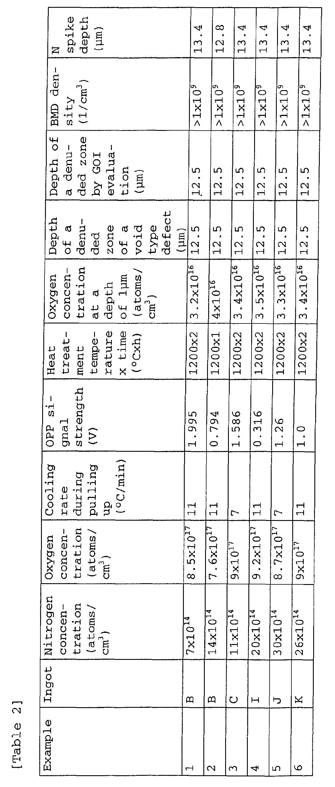
- a semiconductor substrate having a nitrogen concentration of 7x10 14 atoms/cm 3 , an oxygen concentration of 8.5x10 17 atoms/cm 3 and the maximum signal strength of 1.995 V when measuring the micro-defects at the centre of the semiconductor substrate by infrared interference method (OPP) was selected and heat-treated for 2 hours at the temperature of 1200 °C in an atmosphere consisting of a mixture of 50 % hydrogen and 50 % argon.
- the depth of the denuded zone of the void type defect and the depth of denuded zone by GOI evaluation in the semiconductor substrate were both 12.5 ⁇ m
- the oxygen concentration at the centre of the thickness of the semiconductor substrate was 8.5x10 17 atoms/cm 3 or less
- the BMD density was 1x10 9 /cm 3 or more
- the oxygen concentration at the depth of 1 ⁇ m below the surface in the centre of the semiconductor substrate was 3.2x10 16 atoms/cm 3
- the nitrogen spike (N spike) depth was 13.4 ⁇ m.
- the N spike depth of 13.4 ⁇ m means that the locally densified portion produced by nitrogen segregation and exhibiting a signal strength two or more times the average signal strength begins to arise from the depth of 13.4 ⁇ m below the surface of the semiconductor substrate when measuring the concentration of nitrogen by secondary ion mass-spectroscopy (SIMS). Therefore, in the semiconductor substrate after heat-treatment, the depth of the denuded zone of the void type defect and the depth of denuded zone by GOI evaluation are both 12.5 ⁇ m and therefore the depth of the denuded zone is at least 12.5 ⁇ m.
- the term "at least" means that the actual value of polishing was 12.5 ⁇ m in the example and that the denuded zone may possibly be extended to a deeper region. Therefore, the depth of the denuded zone is much deeper than 12 ⁇ m and the depth of the layer region applicable for the production of semiconductor devices is extended by as much as 0.5 ⁇ m, thereby increasing the freedom for the production of semiconductor devices.
- a semiconductor substrate similarly sliced from ingot B shown in Table 1 was used, but a semiconductor substrate, having a nitrogen concentration of 1.4x10 15 atoms/cm 3 , an oxygen concentration of 7.6x10 17 atoms/cm 3 and the maximum signal strength of 0.794 V when measuring the micro-defects at the centre of the semiconductor substrate by infrared interference method (OPP), was used and heat-treated for 1 hour at the temperature of 1200 °C in an atmosphere consisting of a mixture of 50 % hydrogen and 50 % argon.
- OPP infrared interference method
- the depth of the denuded zone of the void type defect and the depth of denuded zone by GOI evaluation were both 12.5 ⁇ m
- the oxygen concentration at the centre of the thickness of the semiconductor substrate was 7.6x10 17 atoms/cm 3 or less
- the BMD density was 1x10 9 /cm 3 or more
- the oxygen concentration at the depth of 1 ⁇ m below the surface in the centre of the semiconductor substrate was 4x10 16 atoms/cm 3
- the N spike depth was 12.8 ⁇ m.
- the N spike depth was lower than that of Example 1 by 0.6 ⁇ m, this is within a range of a measurement error.
- the sliced semiconductor substrate having an oxygen concentration of 9x10 17 atoms/cm 3 , a nitrogen concentration of 11x10 14 atoms/cm 3 and a maximum signal strength of 1.585 V when measured at the centre of the semiconductor substrate by infrared interference method (OPP), was heat-treated for 2 hours at the temperature of 1200 °C in an atmosphere consisting of a mixture of 10 % hydrogen and 90 % argon.
- OPP infrared interference method
- the of the denuded zone depth of the void type defect and the depth of denuded zone by GOI evaluation were both 12.5 ⁇ m
- the oxygen concentration at the centre of the thickness of the semiconductor substrate was 9x10 17 atoms/cm 3 or less
- the BMD density was 1x10 9 /cm 3 or more
- the oxygen concentration at the depth of 1 ⁇ m below the surface in the centre of the semiconductor substrate was 3.4x10 16 atoms/cm 3
- the N spike depth was 13.4 ⁇ m.
- OPP infrared interference method
- the depth of the denuded zone of the void type defect and the depth of denuded zone by GOI evaluation in the semiconductor substrate were both 12.5 ⁇ m, and therefore, the depth of the denuded zone was 12.5 ⁇ m, the oxygen concentration at the centre of the semiconductor substrate was 9.2x10 17 atoms/cm 3 or less, the BMD density was 1x10 19 /cm 3 or more, the oxygen concentration at the depth of 1 ⁇ m below the surface in the centre of the semiconductor substrate was 3.5x10 16 atoms/cm 3 and the N spike depth was 13.4 ⁇ m.
- Example 5 a semiconductor substrate, sliced from ingot J shown in Table 1 and having a nitrogen concentration of 3x10 15 atoms/cm 3 , an oxygen concentration of 8.7x10 17 atoms/cm 3 and the maximum signal strength of 1.26 V when measured at the centre of the semiconductor substrate by infrared interference method (OPP), was used.
- Example 6 a semiconductor substrate, sliced from ingot K shown in Table 1 and having a nitrogen concentration of 2.6x10 15 atoms/cm 3 , an oxygen concentration of 9x10 17 atoms/cm 3 and a maximum signal strength of 1.0 V when measured at the centre of the semiconductor substrate by infrared interference method (OPP), was used.
- each substrate was heat-treated for 2 hours at the temperature of 1200 °C in an atmosphere consisting of 100 % argon.
- the oxygen concentration at the depth of 1 ⁇ m below the surface in the centre of the semiconductor substrate was 3.3x10 16 atoms/cm 3 or 3.4x10 16 atoms/cm 3
- the depth of the denuded zone of the void type defect and the depth of denuded zone by GOI evaluation were both 12.5 ⁇ m
- the depth of the denuded zone (ZD) was 12.5 ⁇ m
- the oxygen concentration at the centre of the thickness of the semiconductor substrate was 8.7x10 17 atoms/cm 3 or less or 8.9x10 17 atoms/cm 3 or less
- the BMD density was 1x10 9 /cm 3 or more
- the N spike depth was 13.4 ⁇ m.
- a semiconductor substrate having a nitrogen concentration of 5x10 14 atoms/cm 3 or more and 1x10 16 atoms/cm 3 or less, an oxygen concentration of 9.5x10 17 atoms/cm 3 or less and a maximum signal strength of 2 V or less when measured at the centre of the semiconductor substrate by infrared interference method (OPP), which is sliced from a silicon single crystal ingot obtained by adjusting the nitrogen concentration of the melt to 5x10 17 atoms/cm 3 or more and 1.5x10 19 atoms/cm 3 or less and by pulling up the ingot while controlling the cooling rate at 5 °C/min or more at the temperature of 1100 °C by the Czochralski method or the magnetic field-applied Czochralski method, is heat-treated for at least one hour at the temperature of 1200 °C or more in a non-oxidising atmosphere.
- the depth of the denuded zone can be made much deeper than 12 ⁇ m, and a silicon semiconductor substrate in which the
- the depth of the denuded zone of the semiconductor substrate is only 7 ⁇ m and even considering only the depth of the denuded zone of the void type defect, a substrate having the depth as low as 7 ⁇ m can be obtained. This is because the nitrogen concentration in the melt and in the semiconductor substrate is zero and the OPP signal strength is too high.
- the oxygen concentration at the depth of 1 ⁇ m of the semiconductor substrate was 3.6x10 16 atoms/cm 3
- the depth of the denuded zone of the void type defect was 7 ⁇ m and the depth of denuded zone by GOI evaluation was 7 ⁇ m
- the BMD density was 1x10 19 /cm 3 or more
- the oxygen concentration at the centre of the thickness of the semiconductor substrate was 9.1x10 17 at-oms/cm 3 or less.
- the depth of the denuded zone of the void type defect and the depth of denuded zone by GOI evaluation are both as low as 7 ⁇ m.
- the oxygen concentration at the depth of 1 ⁇ m of the semiconductor substrate was 3.6x10 16 atoms/cm 3
- the depth of the denuded zone of the void type defect was 10 ⁇ m and the depth of denuded zone by GOI evaluation was 8 ⁇ m
- the BMD density was 1x10 9 /cm 3 or more
- the N spike depth was 13.4 ⁇ m
- the oxygen concentration at the centre of the thickness of the semiconductor substrate was 9.1x10 17 atoms/cm 3 or less.
- the depth of the void type defect and the depth of the denuded zone by GOI evaluation are both as low as 10 ⁇ m. This is considered to be because the cooling rate is low and the OPP signal strength is high as in Comparative Example 2.
- the oxygen concentration at the depth of 1 ⁇ m was 3.7x10 16 atoms/cm 3
- the depth of the denuded zone of the void type defect was 8 ⁇ m
- the depth of denuded zone by GOI evaluation was 8 ⁇ m
- a semiconductor substrate sliced from ingot A was used in the same manner as in Comparative Example 4.
- This comparative example differs from Comparative Example 4 only in the point that the nitrogen concentration was 1.1x10 15 atoms/cm 3 , the oxygen concentration was 9.6x10 17 atoms/cm 3 and the OPP signal strength was 0.301 V, and the atmospheric gas and other heat-treating conditions were the same as in Comparative Example 4.
- the oxygen concentration at the depth of 1 ⁇ m was 3.2x10 16 atoms/cm 3
- the depth of the denuded zone of the void type defect and the depth of denuded zone by GOI evaluation were both as low as 8 ⁇ m
- the BMD density was 5x10 8 /cm 3 or more and the N spike depth was 13.4 ⁇ m.
- the depth of the denuded zone of the semiconductor substrate is therefore as low as 8 ⁇ m is that the nitrogen concentration in the melt is as low as 1.3x10 17 atoms/cm 3 and the nitrogen concentration before heat-treatment is below 2x10 14 at-oms/cm 3 .
- Comparative Example 7 a semiconductor substrate sliced from ingot B shown in Table 1 and having a nitrogen concentration of 7.2x10 14 atoms/cm 3 , an oxygen concentration of 8.5x10 17 atoms/cm 3 and an OPP signal strength of 1.995 V was used.
- Comparative Example 8 a semiconductor substrate sliced from ingot I shown in Table 1 and having a nitrogen concentration of 2.4x10 15 atoms/cm 3 , an oxygen concentration of 9.1x10 17 atoms/cm 3 and an OPP signal strength of 0.50 V was used.
- Comparative Example 9 a semiconductor substrate sliced from ingot K shown in Table 1 and having a nitrogen concentration of 2.5x10 15 atoms/cm 3 , an oxygen concentration of 8.6x10 17 atoms/cm 3 and an OPP signal strength of 1.0 V was used.
- Comparative Example 10 a semiconductor substrate sliced from ingot L shown in Table 1 and having a nitrogen concentration of 2.5x10 15 atoms/cm 3 , an oxygen concentration of 8.2x10 17 atoms/cm 3 and an OPP signal strength of 0.398 V was used.
- the depth of denuded zone of void type defect was 8 ⁇ m
- the depth of denuded zone by GOI evaluation was 6 ⁇ m
- the BMD density was 1x10 9 or more
- the N spike depth was 8 ⁇ m
- the oxygen concentration at the depth of 1 ⁇ m was 3 to 3.4 atoms/cm 3 .
- the depth of the denuded zone of the void type defect and the depth of denuded zone by GOI evaluation are both as low as 10 ⁇ m though the heat-treatment was carried out for as long as 4 hours. This is considered to be because the heat-treating temperature is 1150 °C, which is lower than 1200 °C.
- the oxygen concentration at the depth of 1 ⁇ m was 4.4x10 16 atoms/cm 3
- the depth of the denuded zone of the void type defect was 12.5 ⁇ m
- the depth of denuded zone by GOI evaluation was 9 ⁇ m
- the BMD density was 1x10 9 /cm 3 or more
- the N spike depth was 12.8 ⁇ m
- the oxygen concentration at the centre of the thickness of the semiconductor substrate was 9.5x10 17 atoms/cm 3 or less.
- the depth of the denuded zone of the void type defect is 12.5 ⁇ m, which is greater than 12 ⁇ m
- the depth of denuded zone by GOI evaluation is 9 ⁇ m.
- the N spike depth is 12.8 ⁇ m. Therefore, a locally densified portion produced by nitrogen segregation and exhibiting a signal strength two or more times the average signal strength in the analysis of nitrogen by secondary ion mass-spectroscopy (SIMS) is located at the depth of 12.8 ⁇ m.
- SIMS secondary ion mass-spectroscopy
- the oxygen concentration at the depth of 1 ⁇ m was 4.7x10 16 atoms/cm 3 and the oxygen concentration at the centre of the thickness of the semiconductor substrate was 8.9x10 17 atoms/cm 3 or less.
- the depth of the denuded zone of the void type defect was 12.5 ⁇ m
- the depth of denuded zone by GOI evaluation was 9 ⁇ m
- the BMD density was 1x10 9 /cm 3 or more
- the N spike depth was 12.8 ⁇ m, which are the same as in Example 7.
- Example 10 a semiconductor substrate sliced from ingot J shown in Table 1 and having a nitrogen concentration of 3.1x10 15 atoms/cm 3 , an oxygen concentration of 8.6x10 17 atoms/cm 3 and an OPP signal strength of 1.26 V was used.
- Example 11 a semiconductor substrate sliced from ingot K shown in Table 1 and having a nitrogen concentration of 2.5x10 15 atoms/cm 3 , an oxygen concentration of 9.1x10 17 atoms/cm 3 and an OPP signal strength of 1.585 V was used.
- Example 12 a semiconductor substrate sliced from ingot P shown in Table 1 and having a nitrogen concentration of 6.1x10 17 atoms/cm 3 , an oxygen concentration of 9.2x10 17 atoms/cm 3 and an OPP signal strength of 3.16 V was used.
- Example 7 The heat-treatment of the semiconductor substrates shown in the above Examples 9 to 12 was carried out for one hour at the temperature of 1200 °C in an atmosphere consisting of 25 % hydrogen and 75 % argon, as in Example 7.
- Example 7 the depth of the denuded zone of the void type defect, the depth of denuded zone by GOI evaluation , the N spike depth and the BMD density were quite the same as those of Examples 7 and 8.
- the semiconductor substrates shown in the above Examples 7 to 12 are obtained from a silicon single crystals pulled up at the cooling rate of 5 °C/min at the temperature of 1100 °C using Czochralski method or magnetic field-applied Czochralski method.
- Semiconductor substrates having a nitrogen concentration of 2x10 14 atoms/cm 3 or more and 1x10 16 atoms/cm 3 or less, an oxygen concentration of 9.5x10 17 atoms/cm 3 or less and an OPP signal strength of 4 V or less can be obtained.
- a silicon melt having a nitrogen concentration ranging from 2x10 17 atoms/cm 3 or more and 1.5x10 19 atoms/cm 3 or less is used and the above semiconductor substrates are obtained as a result of heat-treatment performed at least for one hour at the temperature of 1200 °C or more in a non-oxidising atmosphere.
- Comparative Example 12 a semiconductor substrate sliced from ingot G shown in Table 1 and having a nitrogen concentration of 2.5x10 15 atoms/cm 3 , an oxygen concentration of 8.6x10 17 atoms/cm 3 and an OPP signal strength of 1.995 V was used.
- the oxygen concentration at the depth of 1 ⁇ m was 4.5x10 16 atoms/cm 3
- the depth of the denuded zone of the void type defect was 9 ⁇ m
- the depth of denuded zone by GOI evaluation was 9 ⁇ m
- the BMD density was 1x10 9 or more
- the N spike depth was 12.8 ⁇ m.
- the depth of the denuded zone of the void defect and the depth of denuded zone by GOI evaluation were made shallow because the pulling rate of the ingot at the temperature of 1100 °C was less than 5 °C/min.
- the depth of the denuded zone of the void defect and the depth of denuded zone by GOI evaluation are as low as 10 ⁇ m and 8 ⁇ m respectively. This is considered to be because the nitrogen concentration of the semiconductor substrate before being heat-treated does not satisfy the requirement of the lower limit of 2x10 14 atoms/cm 3 .
- the depth of the denuded zone of the void defect and the depth of denuded zone by GOI evaluation are as low as 10 ⁇ m and 6 ⁇ m respectively. This is considered to be because the oxygen concentration of the semiconductor substrate before being heat-treated does not satisfy the requirement of the concentration to be 9.5x10 17 atoms/cm 3 or less.
- the oxygen concentration at the depth of 1 ⁇ m was 3.3x10 16 atoms/cm 3
- the depth of the denuded zone of the void type defect was 8 ⁇ m
- the depth of denuded zone by GOI evaluation was 6 ⁇ m
- the BMD density was 1x10 9 /cm 3 or more
- the N spike depth was 8 ⁇ m. All the depths are considered to be decreased since the heat-treating temperature was 50 °C lower than 1200 °C.
- the depth of the denuded zone is also 12.5 ⁇ m
- the N spike depth is 13.4 ⁇ m or 12.8 ⁇ m
- the semiconductor substrate has a locally densified'portion produced by nitrogen segregation and exhibiting a signal strength two or more times the average signal strength at the depth of 12 ⁇ m or more below the surface thereof when measuring the concentration of nitrogen using secondary ion mass-spectroscopy (SIMS).
- SIMS secondary ion mass-spectroscopy
- the BMD density is greater than 1x10 9 /cm 3 .
- the density at the depth of 1 ⁇ m is at the value of 2.7x10 16 to 3.7x10 16 atoms/cm 3 and the oxygen concentration at the centre of the thickness of the semiconductor substrate is lower than the concentration in the semiconductor substrate before being heat-treated.
- Such an effect as mentioned above can be obtained when the cooling rate at the temperature of 1100 °C is 1 °C/min or more and less than 5 °C/min when pulling up the single crystal and by treating the semiconductor substrate, having an oxygen concentration of 8.5x10 17 atoms/cm 3 or less and a nitrogen concentration of 1x10 15 atoms/cm 3 or more and 1x10 16 atoms/cm 3 or less and an OPP signal strength of 7 V or less, for at least one hour and advantageously one hour to two hours at the temperature of 1200 °C or more and 1300 °C or less in a non-oxidising atmosphere.
- the oxygen concentration is 8.9 atoms/cm 3 to 8.6 atoms/cm 3 , which does not correspond to the condition for the oxygen concentration of 8.5 atoms/cm 3 or less.
- the nitrogen concentration is 7.2x10 14 atoms/cm 3 and 9.1 atoms/cm 3 , which does not correspond to the condition for the lower limit of the nitrogen concentration of 1x10 15 atoms/cm 3 or more.
- the heat-treating temperature is 1150 °C, which does not correspond to the condition for the lower limit of the heat treating temperature of 1200 °C.
- the conditions according to the invention are not selected as the oxygen concentration, nitrogen concentration and heat-treating temperature and time of the semiconductor substrate sliced from a crystal pulled up at the cooling rate of 1 °C/min or more and less than 5 °C/min at the temperature of 1100 °C using Czochralski method or magnetic field-applied Czochralski method, the depth of the denuded zone of the void type defect and the depth of denuded zone by GOI evaluation both do not get the desired value.
- the heat-treating temperature is advantageously 1200 °C or more and 1300 °C or less.
- the heat treatment must be carried out for at least one hour and preferably two hours or less, from the productive point of view.
- a semiconductor substrate by heat-treating a semiconductor substrate for at least one hour at the temperature of 1200 °C in a non-oxidising atmosphere, by selecting the prescribed range of each value of the nitrogen concentration, oxygen concentration and OPP signal strength thereof, wherein the semiconductor substrate is sliced from a silicon single crystal ingot grown by using Czochralski method or magnetic field-applied Czochralski method, where the nitrogen concentration in the melt is selected and where the cooling rate is 5 °C/min or more, or 1 °C or more and less than 5 °C, a semiconductor substrate can be obtained in which the depth of the denuded zone of the void type defect and the depth of denuded zone by GOI evaluation are both made larger than 12 ⁇ m, or the depth of the denuded zone is made larger than 12 ⁇ m and having a locally densified portion produced by nitrogen segregation and exhibiting a signal strength two or more times the average signal strength at a depth of 12 ⁇ m or more below the surface thereof when measuring the concentration of nitrogen by secondary i
Landscapes
- Chemical & Material Sciences (AREA)
- Engineering & Computer Science (AREA)
- Crystallography & Structural Chemistry (AREA)
- Materials Engineering (AREA)
- Metallurgy (AREA)
- Organic Chemistry (AREA)
- Crystals, And After-Treatments Of Crystals (AREA)
- Liquid Deposition Of Substances Of Which Semiconductor Devices Are Composed (AREA)
Abstract
Description
- D:
- Diffusion constant of oxygen at the temperature of 1200 °C
- c0:
- Concentration of oxygen at the centre of the thickness of the wafer
- t:
- Heat treating time at the temperature of 1200 °C or more
- x:
- Depth from the surface.
void volume V (nm3) = 20000x(OPP maximum signal strength)1.6.
void volume V (nm3) = 110x(OPP maximum signal strength)3.6.
If the results of GOI are more than 90 % yield, the results of repeated cleaning using SC1 are less than 2x10⁵/cm3 but converses do not always consist.



Claims (9)
- A silicon semiconductor wafer obtained from a silicon single crystal grown by a method selected from the group consisting of Czochralski method and a magnetic field-applied Czochralski method, the silicon semiconductor wafer comprising, after heat-treatment in a non-oxidising atmosphere, a denuded zone with a depth of at least 12 µm and a crystal defect density of oxygen precipitates of at least 5x10⁸/cm3 at a centre of a thickness of the silicon semiconductor wafer.
- A silicon semiconductor wafer according to Claim 1, wherein a concentration of oxygen at a depth of 1 µm below a surface in a centre of the silicon semiconductor wafer is up to 5x10¹⁶ atoms/cm3 and the concentration of oxygen at the centre of the thickness of the silicon semiconductor wafer is up to 9.5x10¹⁷ atoms/cm3, said silicon semiconductor wafer being obtained after heat-treating, in a non-oxidising atmosphere, a silicon wafer that has an oxygen concentration of up to 9.5x10¹⁷ atoms/cm3, a nitrogen concentration in the range from 5x10¹⁴ atoms/cm3 to 1x10¹⁶ atoms/cm3, and a maximum signal strength measured at the centre thereof by infrared interference method (OPP) of up to 2 V.
- A silicon semiconductor wafer according to Claim 1, wherein a concentration of oxygen at a depth of 1 µm below a surface in a centre of the silicon semiconductor wafer is up to 5x10¹⁶ atoms/cm3 and the concentration of oxygen at the centre of the thickness of the silicon semiconductor wafer is up to 8.5x10¹⁷ atoms/cm3, said silicon semiconductor wafer being obtained after heat-treating, in a non-oxidising atmosphere, a silicon wafer that has an oxygen concentration of up to 8.5x10¹⁷ atoms/cm3, a nitrogen concentration in the range from 1x10¹⁵ atoms/cm3 to 1x10¹⁶ atoms/cm3, and a maximum signal strength measured at the centre thereof by infrared interference method (OPP) of up to 7 V.
- A silicon semiconductor wafer which has been subject to a heat-treatment in a non-oxidising atmosphere, characterised by an oxygen concentration at a centre of a thickness of the silicon semiconductor wafer of up to 9.5x10¹⁷ atoms/cm3, a locally densified portion produced by nitrogen segregation and exhibiting a signal strength at least two times an average signal strength at a depth of at least 12 µm below a surface thereof when measuring a concentration of nitrogen by secondary ion mass spectroscopy (SIMS), a depth of a denuded zone of a void type defect of at least 12 µm, and a crystal defect density of oxygen precipitates at a centre of a thickness thereof of at least 5x10⁸/cm3.
- A silicon semiconductor wafer according to Claim 4, characterised by a concentration of oxygen at a depth of 1 µm below a surface in a centre of the silicon semiconductor wafer of up to 5x10¹⁶ atoms/cm3 and a concentration of oxygen at the centre of the thickness of the silicon semiconductor wafer of up to 9.5x10¹⁷ atoms/cm3, said silicon semiconductor wafer being obtained by heat-treatment, in a non-oxidising atmosphere, a silicon wafer that has an oxygen concentration of up to 9.5x10¹⁷ atoms/cm3, a nitrogen concentration in the range from 2x10¹⁴ atoms/cm3 to 1x10¹⁶ atoms/cm3, and a maximum signal strength of which measured at the centre thereof by infrared interference method (OPP) of up to 4 V.
- A silicon semiconductor wafer according to Claim 4, characterised by a concentration of oxygen at a depth of 1 µm below a surface in a centre of the silicon semiconductor wafer of up to 5x10¹⁶ atoms/cm3 and a concentration of oxygen at the centre of the thickness of the silicon semiconductor wafer of up to 8.5x10¹⁷ atoms/cm3, said silicon semiconductor wafer being obtained by heat-treatment, in a non-oxidising atmosphere, a silicon wafer that is obtained from a silicon single crystal (ingot) having been pulled up, and that has an oxygen concentration of up to 8.5x10¹⁷ atoms/cm3, a nitrogen concentration in the range from 1x10¹⁵ atoms/cm3 to 1x10¹⁶ atoms/cm3, and a maximum signal strength of which measured at the centre thereof by an infrared interference method (OPP) of up to 7 V.
- A process for producing a silicon semiconductor wafer, comprising
growing a silicon single crystal under the conditions of a cooling rate of at least 5 °C/minute at the temperature of 1100 °C, by using a silicon melt containing at least 5x10¹⁷ atoms/cm3 and up to 1.5x10¹⁹ atoms/cm3 of nitrogen, through the Czochralski method or a magnetic field-applied Czochralski method,
slicing a silicon wafer from said silicon single crystal, the silicon wafer having an oxygen concentration of up to 9.5x10¹⁷ atoms/cm3,
and heat-treating the silicon wafer for at least one hour at a temperature of at least 1200 °C in a non-oxidising atmosphere. - A process for producing a silicon semiconductor wafer, comprising
growing a silicon single crystal under the conditions of a cooling rate of at least 5 °C/minute at the temperature of 1100 °C, by using a silicon melt containing at least 2x10¹⁷ atoms/cm3 and up to 1.5x10¹⁹ atoms/cm3 of nitrogen, through the Czochralski method or a magnetic field-applied Czochralski method,
slicing a silicon wafer from said silicon single crystal, the silicon wafer having an oxygen concentration of up to 9.5x10¹⁷ atoms/cm3,
and heat-treating the silicon wafer for at least one hour at a temperature of at least 1200 °C in a non-oxidising atmosphere. - A process for producing a silicon semiconductor wafer, comprising
growing a silicon single crystal under the conditions of a cooling rate of at least 1 °C/minute and up to 5 °/minute at the temperature of 1100 °C, by using a silicon melt containing at least 1x10¹⁸ atoms/cm3 and up to 1.5x10¹⁹ atoms/cm3 of nitrogen, through the Czochralski method or a magnetic field-applied Czochralski method,
slicing a silicon wafer from said silicon single crystal, the silicon wafer having an oxygen concentration of up to 8.5x10¹⁷ atoms/cm3,
and heat-treating the silicon wafer for at least one hour at a temperature of at least 1200 °C in a non-oxidising atmosphere.
Applications Claiming Priority (2)
| Application Number | Priority Date | Filing Date | Title |
|---|---|---|---|
| JP2001242498 | 2001-08-09 | ||
| JP2001242498A JP4566478B2 (en) | 2001-08-09 | 2001-08-09 | Silicon semiconductor substrate and manufacturing method thereof |
Publications (3)
| Publication Number | Publication Date |
|---|---|
| EP1284311A2 true EP1284311A2 (en) | 2003-02-19 |
| EP1284311A3 EP1284311A3 (en) | 2003-03-05 |
| EP1284311B1 EP1284311B1 (en) | 2006-02-08 |
Family
ID=19072759
Family Applications (1)
| Application Number | Title | Priority Date | Filing Date |
|---|---|---|---|
| EP02017733A Expired - Lifetime EP1284311B1 (en) | 2001-08-09 | 2002-08-08 | Silicon semiconductor substrate and process for producing the same |
Country Status (7)
| Country | Link |
|---|---|
| US (1) | US6805742B2 (en) |
| EP (1) | EP1284311B1 (en) |
| JP (1) | JP4566478B2 (en) |
| KR (1) | KR100487935B1 (en) |
| CN (1) | CN1237586C (en) |
| DE (1) | DE60209064T2 (en) |
| TW (1) | TW565896B (en) |
Cited By (3)
| Publication number | Priority date | Publication date | Assignee | Title |
|---|---|---|---|---|
| US8545622B2 (en) | 2005-12-27 | 2013-10-01 | Siltronic Ag | Annealed wafer and manufacturing method of annealed wafer |
| CN107615470A (en) * | 2015-05-20 | 2018-01-19 | 信越半导体株式会社 | The manufacture method and evaluation method of silicon epitaxial wafer |
| EP4151782A1 (en) * | 2021-09-16 | 2023-03-22 | Siltronic AG | Single crystal silicon semiconductor wafer and method of manufacturing a single crystal silicon semiconductor wafer |
Families Citing this family (16)
| Publication number | Priority date | Publication date | Assignee | Title |
|---|---|---|---|---|
| JP4615161B2 (en) * | 2001-08-23 | 2011-01-19 | 信越半導体株式会社 | Epitaxial wafer manufacturing method |
| JP4567251B2 (en) * | 2001-09-14 | 2010-10-20 | シルトロニック・ジャパン株式会社 | Silicon semiconductor substrate and manufacturing method thereof |
| JP4396640B2 (en) * | 2004-02-03 | 2010-01-13 | 信越半導体株式会社 | Semiconductor wafer manufacturing method and semiconductor ingot cutting position determination system |
| KR100705939B1 (en) | 2004-08-26 | 2007-04-11 | 주식회사 하이닉스반도체 | Semiconductor Wafer Manufacturing Method |
| JP2006273631A (en) * | 2005-03-28 | 2006-10-12 | Komatsu Electronic Metals Co Ltd | Silicon single crystal manufacturing method, annealed wafer, and annealed wafer manufacturing method |
| JP4997829B2 (en) * | 2006-05-25 | 2012-08-08 | 株式会社デンソー | Manufacturing method of semiconductor device |
| JP5119677B2 (en) | 2007-02-16 | 2013-01-16 | 株式会社Sumco | Silicon wafer and manufacturing method thereof |
| WO2008154593A1 (en) * | 2007-06-11 | 2008-12-18 | Smith & Nephew, Inc. | Ceramic layered medical implant |
| DE102007056115A1 (en) * | 2007-11-15 | 2009-05-20 | Freiberger Compound Materials Gmbh | Process for separating single crystals |
| JP5304206B2 (en) * | 2008-12-04 | 2013-10-02 | 信越半導体株式会社 | Single crystal manufacturing method and single crystal manufacturing apparatus |
| JP5346744B2 (en) * | 2008-12-26 | 2013-11-20 | ジルトロニック アクチエンゲゼルシャフト | Silicon wafer and manufacturing method thereof |
| EP2309038B1 (en) * | 2009-10-08 | 2013-01-02 | Siltronic AG | production method of an epitaxial wafer |
| US9945048B2 (en) | 2012-06-15 | 2018-04-17 | Taiwan Semiconductor Manufacturing Company, Ltd. | Semiconductor structure and method |
| CN105297140B (en) * | 2015-09-10 | 2019-10-25 | 上海超硅半导体有限公司 | Silicon wafer and annealing method |
| JP6711320B2 (en) * | 2017-06-26 | 2020-06-17 | 株式会社Sumco | Silicon wafer |
| KR102003506B1 (en) | 2018-12-17 | 2019-07-24 | ㈜엔텍 | Seismic strengthening mortar composition with high toughness and self-healing function and repair and reinforcement method of concrete structure using the same |
Family Cites Families (9)
| Publication number | Priority date | Publication date | Assignee | Title |
|---|---|---|---|---|
| GB2080780B (en) | 1980-07-18 | 1983-06-29 | Secr Defence | Heat treatment of silicon slices |
| US4437922A (en) | 1982-03-26 | 1984-03-20 | International Business Machines Corporation | Method for tailoring oxygen precipitate particle density and distribution silicon wafers |
| JPH0786289A (en) | 1993-07-22 | 1995-03-31 | Toshiba Corp | Semiconductor silicon wafer and manufacturing method thereof |
| US5994761A (en) * | 1997-02-26 | 1999-11-30 | Memc Electronic Materials Spa | Ideal oxygen precipitating silicon wafers and oxygen out-diffusion-less process therefor |
| TW589415B (en) | 1998-03-09 | 2004-06-01 | Shinetsu Handotai Kk | Method for producing silicon single crystal wafer and silicon single crystal wafer |
| JP3975605B2 (en) | 1998-11-17 | 2007-09-12 | 信越半導体株式会社 | Silicon single crystal wafer and method for producing silicon single crystal wafer |
| JP2000281490A (en) * | 1999-03-26 | 2000-10-10 | Nippon Steel Corp | Silicon semiconductor substrate and method of manufacturing the same |
| JP3903655B2 (en) * | 1999-08-11 | 2007-04-11 | 株式会社Sumco | IG processing method of silicon wafer |
| JP3994602B2 (en) * | 1999-11-12 | 2007-10-24 | 信越半導体株式会社 | Silicon single crystal wafer, manufacturing method thereof, and SOI wafer |
-
2001
- 2001-08-09 JP JP2001242498A patent/JP4566478B2/en not_active Expired - Lifetime
-
2002
- 2002-08-06 KR KR10-2002-0046355A patent/KR100487935B1/en not_active Expired - Lifetime
- 2002-08-07 US US10/213,470 patent/US6805742B2/en not_active Expired - Lifetime
- 2002-08-08 EP EP02017733A patent/EP1284311B1/en not_active Expired - Lifetime
- 2002-08-08 DE DE60209064T patent/DE60209064T2/en not_active Expired - Lifetime
- 2002-08-08 TW TW091117930A patent/TW565896B/en not_active IP Right Cessation
- 2002-08-09 CN CNB021285306A patent/CN1237586C/en not_active Expired - Lifetime
Cited By (6)
| Publication number | Priority date | Publication date | Assignee | Title |
|---|---|---|---|---|
| US8545622B2 (en) | 2005-12-27 | 2013-10-01 | Siltronic Ag | Annealed wafer and manufacturing method of annealed wafer |
| CN107615470A (en) * | 2015-05-20 | 2018-01-19 | 信越半导体株式会社 | The manufacture method and evaluation method of silicon epitaxial wafer |
| CN107615470B (en) * | 2015-05-20 | 2020-06-19 | 信越半导体株式会社 | Manufacturing method and evaluation method of silicon epitaxial wafer |
| EP4151782A1 (en) * | 2021-09-16 | 2023-03-22 | Siltronic AG | Single crystal silicon semiconductor wafer and method of manufacturing a single crystal silicon semiconductor wafer |
| WO2023041359A1 (en) * | 2021-09-16 | 2023-03-23 | Siltronic Ag | Process for manufacturing a monocrystalline silicon semiconductor wafer, and monocrystalline silicon semiconductor wafer |
| US12680189B2 (en) | 2021-09-16 | 2026-07-14 | Siltronic Ag | Process for manufacturing a monocrystalline silicon semiconductor wafer, and monocrystalline silicon semiconductor wafer |
Also Published As
| Publication number | Publication date |
|---|---|
| EP1284311A3 (en) | 2003-03-05 |
| TW565896B (en) | 2003-12-11 |
| CN1402317A (en) | 2003-03-12 |
| EP1284311B1 (en) | 2006-02-08 |
| US6805742B2 (en) | 2004-10-19 |
| JP2003055088A (en) | 2003-02-26 |
| DE60209064T2 (en) | 2006-07-13 |
| KR20030014602A (en) | 2003-02-19 |
| KR100487935B1 (en) | 2005-05-03 |
| CN1237586C (en) | 2006-01-18 |
| DE60209064D1 (en) | 2006-04-20 |
| JP4566478B2 (en) | 2010-10-20 |
| US20030079674A1 (en) | 2003-05-01 |
Similar Documents
| Publication | Publication Date | Title |
|---|---|---|
| EP1284311B1 (en) | Silicon semiconductor substrate and process for producing the same | |
| KR100581047B1 (en) | Method of manufacturing silicon single crystal wafer and silicon single crystal wafer | |
| KR100582240B1 (en) | Silicon single crystal wafer and a method for producing it | |
| EP1143045B1 (en) | Silicon single crystal wafer for epitaxial wafer, epitaxial wafer and methods for producing the same and evaluating the same | |
| EP1887110B1 (en) | Silicon single crystal manufacturing method and silicon wafer | |
| US6599360B2 (en) | Silicon wafer, method for determining production conditions of silicon single crystal and method for producing silicon wafer | |
| JP3975605B2 (en) | Silicon single crystal wafer and method for producing silicon single crystal wafer | |
| EP1229155A1 (en) | Silicon wafer, silicon epitaxial wafer, anneal wafer and method for producing them | |
| US6632411B2 (en) | Silicon wafer and method for producing silicon single crystal | |
| WO2000031324A1 (en) | Single-crystal silicon wafer having few crystal defects and method for manufacturing the same | |
| KR100566824B1 (en) | Silicon semiconductor substrate and preparation thereof | |
| EP1536044B1 (en) | Method of manufacturing an epitaxial silicon wafer | |
| EP1308544A1 (en) | SILICON SINGLE CRYSTAL WAFER HAVING VOID DENUDED ZONE ON THE SUFRACE AND DIAMETER OF ABOVE 300 mm AND ITS PRODUCTION METHOD | |
| US6179910B1 (en) | Method for manufacturing silicon single crystals and wafers adapted for producing semiconductors | |
| US20090061140A1 (en) | Silicon Single Crystal Producing Method, Annealed Wafer, and Method of Producing Annealed Wafer | |
| US7071079B2 (en) | Epitaxial wafer and a method for producing it | |
| KR20070069040A (en) | Annealed Wafers and Methods of Making Annealed Wafers | |
| KR100445190B1 (en) | Manufacturing method of silicon single crystal ingot | |
| US6579589B1 (en) | Semiconductor wafer with crystal lattice defects, and process for producing this semiconductor wafer | |
| EP1127962B1 (en) | Method for manufacturing silicon single crystal, silicon single crystal manufactured by the method, and silicon wafer | |
| US12497710B2 (en) | Method for producing semiconductor wafers | |
| JP3452042B2 (en) | Silicon wafer manufacturing method | |
| US7122082B2 (en) | Silicon wafer and manufacturing method thereof | |
| JP2002134513A (en) | Heat treatment method for silicon wafer |
Legal Events
| Date | Code | Title | Description |
|---|---|---|---|
| PUAI | Public reference made under article 153(3) epc to a published international application that has entered the european phase |
Free format text: ORIGINAL CODE: 0009012 |
|
| PUAL | Search report despatched |
Free format text: ORIGINAL CODE: 0009013 |
|
| 17P | Request for examination filed |
Effective date: 20020808 |
|
| AK | Designated contracting states |
Designated state(s): AT BE BG CH CY CZ DE DK EE ES FI FR GB GR IE IT LI LU MC NL PT SE SK TR |
|
| AX | Request for extension of the european patent |
Extension state: AL LT LV MK RO SI |
|
| AK | Designated contracting states |
Kind code of ref document: A3 Designated state(s): AT BE BG CH CY CZ DE DK EE ES FI FR GB GR IE IT LI LU MC NL PT SE SK TR |
|
| AX | Request for extension of the european patent |
Extension state: AL LT LV MK RO SI |
|
| RIC1 | Information provided on ipc code assigned before grant |
Ipc: 7C 30B 15/00 B Ipc: 7H 01L 21/322 A Ipc: 7C 30B 33/00 B Ipc: 7C 30B 29/06 B |
|
| 17Q | First examination report despatched |
Effective date: 20030305 |
|
| AKX | Designation fees paid |
Designated state(s): DE |
|
| RAP1 | Party data changed (applicant data changed or rights of an application transferred) |
Owner name: SILTRONIC AG |
|
| GRAP | Despatch of communication of intention to grant a patent |
Free format text: ORIGINAL CODE: EPIDOSNIGR1 |
|
| GRAS | Grant fee paid |
Free format text: ORIGINAL CODE: EPIDOSNIGR3 |
|
| GRAA | (expected) grant |
Free format text: ORIGINAL CODE: 0009210 |
|
| AK | Designated contracting states |
Kind code of ref document: B1 Designated state(s): DE |
|
| REF | Corresponds to: |
Ref document number: 60209064 Country of ref document: DE Date of ref document: 20060420 Kind code of ref document: P |
|
| PLBE | No opposition filed within time limit |
Free format text: ORIGINAL CODE: 0009261 |
|
| STAA | Information on the status of an ep patent application or granted ep patent |
Free format text: STATUS: NO OPPOSITION FILED WITHIN TIME LIMIT |
|
| 26N | No opposition filed |
Effective date: 20061109 |
|
| PGFP | Annual fee paid to national office [announced via postgrant information from national office to epo] |
Ref country code: DE Payment date: 20210819 Year of fee payment: 20 |
|
| REG | Reference to a national code |
Ref country code: DE Ref legal event code: R071 Ref document number: 60209064 Country of ref document: DE |