EP1283588A2 - Inductance à valeur commandable par commutation - Google Patents
Inductance à valeur commandable par commutation Download PDFInfo
- Publication number
- EP1283588A2 EP1283588A2 EP02291997A EP02291997A EP1283588A2 EP 1283588 A2 EP1283588 A2 EP 1283588A2 EP 02291997 A EP02291997 A EP 02291997A EP 02291997 A EP02291997 A EP 02291997A EP 1283588 A2 EP1283588 A2 EP 1283588A2
- Authority
- EP
- European Patent Office
- Prior art keywords
- circuit
- switching
- value
- rectifier
- phases
- Prior art date
- Legal status (The legal status is an assumption and is not a legal conclusion. Google has not performed a legal analysis and makes no representation as to the accuracy of the status listed.)
- Withdrawn
Links
- 238000004804 winding Methods 0.000 claims abstract description 77
- 238000009877 rendering Methods 0.000 claims description 2
- 230000001939 inductive effect Effects 0.000 abstract description 4
- 230000007423 decrease Effects 0.000 description 7
- 229920006395 saturated elastomer Polymers 0.000 description 7
- 238000011144 upstream manufacturing Methods 0.000 description 6
- 230000009467 reduction Effects 0.000 description 5
- 230000008901 benefit Effects 0.000 description 3
- 230000010349 pulsation Effects 0.000 description 3
- 230000002238 attenuated effect Effects 0.000 description 2
- 230000008859 change Effects 0.000 description 2
- 230000001627 detrimental effect Effects 0.000 description 2
- 230000010363 phase shift Effects 0.000 description 2
- 230000007704 transition Effects 0.000 description 2
- 229910000859 α-Fe Inorganic materials 0.000 description 2
- XUIMIQQOPSSXEZ-UHFFFAOYSA-N Silicon Chemical compound [Si] XUIMIQQOPSSXEZ-UHFFFAOYSA-N 0.000 description 1
- 230000001174 ascending effect Effects 0.000 description 1
- 230000008033 biological extinction Effects 0.000 description 1
- 150000001875 compounds Chemical class 0.000 description 1
- 230000008878 coupling Effects 0.000 description 1
- 238000010168 coupling process Methods 0.000 description 1
- 238000005859 coupling reaction Methods 0.000 description 1
- 230000003247 decreasing effect Effects 0.000 description 1
- 230000000694 effects Effects 0.000 description 1
- 238000001914 filtration Methods 0.000 description 1
- 238000005304 joining Methods 0.000 description 1
- 239000000696 magnetic material Substances 0.000 description 1
- 238000004519 manufacturing process Methods 0.000 description 1
- 238000005457 optimization Methods 0.000 description 1
- 230000000737 periodic effect Effects 0.000 description 1
- 230000035699 permeability Effects 0.000 description 1
- 229910052710 silicon Inorganic materials 0.000 description 1
- 239000010703 silicon Substances 0.000 description 1
- 238000001228 spectrum Methods 0.000 description 1
- 230000001629 suppression Effects 0.000 description 1
- 230000001360 synchronised effect Effects 0.000 description 1
Images


Classifications
-
- H—ELECTRICITY
- H02—GENERATION; CONVERSION OR DISTRIBUTION OF ELECTRIC POWER
- H02M—APPARATUS FOR CONVERSION BETWEEN AC AND AC, BETWEEN AC AND DC, OR BETWEEN DC AND DC, AND FOR USE WITH MAINS OR SIMILAR POWER SUPPLY SYSTEMS; CONVERSION OF DC OR AC INPUT POWER INTO SURGE OUTPUT POWER; CONTROL OR REGULATION THEREOF
- H02M1/00—Details of apparatus for conversion
- H02M1/12—Arrangements for reducing harmonics from AC input or output
-
- H—ELECTRICITY
- H02—GENERATION; CONVERSION OR DISTRIBUTION OF ELECTRIC POWER
- H02M—APPARATUS FOR CONVERSION BETWEEN AC AND AC, BETWEEN AC AND DC, OR BETWEEN DC AND DC, AND FOR USE WITH MAINS OR SIMILAR POWER SUPPLY SYSTEMS; CONVERSION OF DC OR AC INPUT POWER INTO SURGE OUTPUT POWER; CONTROL OR REGULATION THEREOF
- H02M7/00—Conversion of AC power input into DC power output; Conversion of DC power input into AC power output
- H02M7/02—Conversion of AC power input into DC power output without possibility of reversal
- H02M7/04—Conversion of AC power input into DC power output without possibility of reversal by static converters
- H02M7/12—Conversion of AC power input into DC power output without possibility of reversal by static converters using discharge tubes with control electrode or semiconductor devices with control electrode
- H02M7/145—Conversion of AC power input into DC power output without possibility of reversal by static converters using discharge tubes with control electrode or semiconductor devices with control electrode using devices of a thyratron or thyristor type requiring extinguishing means
- H02M7/155—Conversion of AC power input into DC power output without possibility of reversal by static converters using discharge tubes with control electrode or semiconductor devices with control electrode using devices of a thyratron or thyristor type requiring extinguishing means using semiconductor devices only
- H02M7/162—Conversion of AC power input into DC power output without possibility of reversal by static converters using discharge tubes with control electrode or semiconductor devices with control electrode using devices of a thyratron or thyristor type requiring extinguishing means using semiconductor devices only in a bridge configuration
- H02M7/1623—Conversion of AC power input into DC power output without possibility of reversal by static converters using discharge tubes with control electrode or semiconductor devices with control electrode using devices of a thyratron or thyristor type requiring extinguishing means using semiconductor devices only in a bridge configuration with control circuit
Definitions
- the invention lies in the field of circuits with an inductance which can be made vary the value between a first nominal value and a second value. It concerns, in particular, a supply circuit comprising such inductors in series with a rectifier bridge.
- Switching at circuit level rectifiers cause switch notches in the voltage between phases of the supply circuit.
- the influence of these switching notches in electrical circuits supplied by the same network as the one supplying the rectifier and located upstream of rectifiers, is felt all the more strongly at circuit level of another user, than the circuit of this other user is closer to the rectifier.
- the presence of these switch notches is detrimental to the proper functioning of certain devices and therefore limit their level. To this end, it is known to put in place series with the rectifier, inductors which are intended to reduce the depth of said notches switching.
- inductances intended to amortize the switching notches serve their purpose well. However, they have a disadvantage in that made of their presence, they create a fall of inductive voltage upstream of the rectifier which therefore is continuously powered by a higher voltage scaled down. In addition for various reasons, these inductors are generally air inductors (coreless magnetic) and thereby obtaining a value desired requires a winding having a large number of turns.
- the duration of the switching with respect to switching cycle is necessarily very short. For an optimization of the supply circuit it should therefore benefit from the presence of chokes during switching times, and remove said inductors apart from these said moments.
- the present invention does not remove physically the presence of windings forming inductance outside the switching times, but it makes it possible to cancel the value of the inductances during periods of time outside the durations of switching. It follows that with this invention, the inductor only loads the rectifier circuit only during switching moments and only charges it not outside of these moments.
- the inductance that we want delete consists of a circuit comprising a primary winding and a secondary winding, this secondary winding being coupled to the winding primary, for example, by the presence of a circuit magnetic.
- the secondary winding is connected to a load impedance.
- the inductance thus constituted by the primary and secondary windings and by load impedance is also connected in parallel on a switching means having an input control, allowing to short-circuit the secondary winding and thereby short circuit inductance seen from the primary. So during all the periods when we want to cancel inductance, the switching means of so that the secondary winding is short-circuited. On the contrary when we need to inductance, for example to reduce the depth switching notches the switching means is ordered in an open position.
- the invention relates to a electrical circuit comprising an inductance, inductor comprising a coupled primary winding magnetically to a secondary winding charged by a load impedance connected in parallel on said secondary winding, circuit characterized in that that it includes a switching means having an input control, connected in parallel on the winding secondary, said switching means being capable of two states, a passing state in which the winding secondary is shorted so the value of the inductance is canceled and a non-passing state in which the inductor has a nominal value desired.
- the switching means comprises, a half-wave rectifier means placed parallel to the secondary winding.
- This characteristic allows having only one sense of passage of current in a branch of the means of switching connected in parallel on the winding secondary, this branch of the switching means comprising a switch which is thus connected in parallel on the secondary winding. Because the direction of passage in this branch is unique it is possible if the switch is a component letting the current flow only in one direction, as for example a transistor, to have only one switch in the switching circuit.
- This switch can be for example a transistor or preferably an insulated gate bipolar transistor (IGBT Isolated Gate Bipolar Transistor).
- the inductance load impedance can be adjustable.
- the coupling between the winding primary and secondary winding is performed at by means of a magnetic circuit for example in the form of ferrite or other magnetic material.
- a magnetic circuit for example in the form of ferrite or other magnetic material.
- inductive circuit conforms to the invention can be saturable, which presents advantages which will be explained below, on the form and filtering the switch notches.
- a circuit according to the invention can be used to form, upstream of a rectifier circuit, an inductor to reduce the depth of switching slots.
- the control of the switching means in parallel on the secondary winding of the reduction inductor of the depth of the switch notches either synchronized with the switching command of a rectifier connected in series with said inductor to be non passing only during the short duration of the switching of this rectifier.
- Such use may relate to example a hexaphase rectifier with thyristors on a load said rectifier being itself supplied by a three-phase alternative network.
- each of inductors is inserted into each phases between the network and the rectifier.
- a trigger from each of rectifier thyristors receives a logic signal from command enabling the thyristor to be turned on at appropriate times.
- Naturally use is not limited to a six-phase rectifier powered by a three-phase network.
- the use of the invention relates to a supply circuit for a load from a polyphase source comprising on each supply phase an inductor connected in series with a compound rectifier assembly rectifiers, each rectifier in the set having a control input receiving a first signal control logic, said first logic signal controlling the passing state of said rectifiers, circuit supply of a load characterized in that each of the inductors is formed by a winding primary magnetically coupled to a winding secondary charged by a load resistor connected in parallel on said winding secondary, the secondary winding of this inductor being connected in parallel on a means of switching having a control input, said means switch capable of two states, one state passer-by in which the secondary winding is short-circuited so that the value of the inductance is found canceled and a non-passing state in which the inductor has a desired nominal value, the switching means being on or off depending on the value of a second logic signal applied to this switching input control input, the second logic signal being delivered by means of synchronization developing the second logic signal
- each inductor of reduction of notches is constituted by a circuit according to one of the embodiments of the invention, the switching means of each circuit according to one embodiments of the invention being passing or not passing according to the value of a second signal logic applied to its command input, the second logic signal being delivered by means of synchronization to make non passing during the switching of a rectifier, switching means of the circuit according to one of the embodiments of the invention connected to one of the supply phases.
- each of the supply phases is connected in series with a branch of a double rectifier bridge alternation formed by a set of rectifiers, each rectifier having a command input receiving a first control logic signal, said first logic signal controlling the passing state of said rectifiers, load supply circuit characterized in that it comprises on each of the phases, a circuit according to one of the forms of embodiment of the invention, the switching means of each circuit according to one of the embodiments of the invention being passing or not passing according to the value of a second logic signal applied to its input switching command, the second logic signal being delivered by synchronization means synchronizing the second logic signal to make non passing during the switching of a rectifier, the means for switching two circuits according to one of embodiments of the invention.
- Switching means of circuits according to one of the embodiments of the invention which are simultaneously turned off during the switching of a rectifier assigned to a phase are those assigned to said phase, are the circuit assigned to said phase and those assigned to another phase which is found during short circuit switching with said phase.
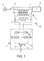
- FIG. 1 represents an electrical circuit 20 according to the invention.
- a power supply 10 for example a network supplying a sinusoidal current, is connected through a switch 9 to a winding primary 3 itself coupled in series to an impedance of load Z 15.
- a winding secondary 4 is coupled through a circuit magnetic 5 for example in silicon sheet or ferrite at the primary winding 3.
- a resistor 6, is connected in parallel on the secondary winding 4.
- the primary winding 3, the magnetic circuit 5, secondary winding 4, resistor 6 form together an inductance 2.
- the inductance 2 thus formed is equivalent to a transformer of current. With resistor 6 thus connected the secondary of this transformer, formed by secondary winding 4 is never completely open.
- this resistor 6 is chosen so that the terminal voltage of secondary winding 4 never exceeds one fixed value, for example a few hundred volts
- switching means 1 is connected in parallel on the secondary winding 4.
- the means switch 1 has a control input 81 which allows to make the switching means 1 on or off passing.
- inductance 2 has a determined value to absorb any fluctuations or switching slots on a circuit comprising said primary winding 3.
- the circuit consists of said inductance 2 and load 15.
- inductance 2 when the switching means 1 is controlled passing, inductance 2 then has a value which is canceled out since the current passes through the switching means 1 which short-circuits the winding secondary 4 and therefore the value of inductance 2 is reduced to a negligible value in the circuit comprising it.
- the switching means 1 comprises a means full-wave rectifier 7, for example in the form a diode bridge, coupled in parallel to the secondary winding 4.
- a switch 8 under form, for example, of an IGBT, is present in a branch 14 of the switching means 1 connected at parallel to rectifier means 7 and to the winding secondary 4.
- the rectifier means 7 allows the current passing through the collector emitter path of the IGBT 8 to always be in the same direction whatever let the polarities of the current across the terminals of secondary winding 4. In this way it is possible use only one switch 8.
- This figure represents a circuit power supply 100 of a load Z 15.
- the charge Z 15 is formed by a rectifier bridge 50, for example a bridge Graetz or Larionov connected in series with a load 16.
- the circuit 100 includes a current source 10 three-phase AC having 3 phases 11, 12, 13 designated generally by R, S, T respectively. It will be in general of the phases of a three-phase supply network.
- Each of the phases is provided with a circuit 27, 28, 29 respectively, designed as the circuit 20 described in conjunction with Figure 1.
- Figure 2 In order not to overload Figure 2, it has only been shown completely in this figure only one circuit 27 connected on the phase 11. It should however be understood that each of the two other phases 12 and 13 is provided in the same way of a similar circuit 28, 29 respectively.
- the representation of only the primary windings 32, 33 circuits 28, 29 is sufficient for understanding of the device shown in Figure 2.
- the references of items not shown appear in parentheses at side of the similar element shown.
- Each of phases 11, 12, 13 of source 10 is connected respectively to a primary winding 31, 32, 33 of an inductor 21, 22, 23.
- Each of the inductors 21, 22, 23 is formed like inductance 2 described in relation to Figure 1. This means that each of the inductors 21, 22, 23 comprises in addition to the primary winding 31, 32, 33 respectively one secondary winding 47, 48, 49 magnetically coupled to the primary winding 31, 32, 33 respectively.
- a resistor 67, 68, 69 is connected in parallel on each of the secondary windings 47, 48, 49.
- switching means 17, 18, 19 having an input of command 84, 85, 86 respectively is connected by parallel on each of the secondary windings 47, 48, 49 respectively.
- the switching means 17 has a branch 71 connected in parallel on the winding secondary 47.
- each means of switching 17-19 comprises as shown in FIG.
- Each of the primary windings 31, 32, 33 is connected to the rectifier bridge 50 which is formed in three branches 57, 58, 59.
- the first winding 31 of the first phase 11 is connected to a first branch 57 at a first point of connection 24.
- Rectifiers in the example here commented on thyristors 51, 62 each provided with a state command input 54, 66 respectively, in the example here commented on it is a thyristor control trigger, are arranged on branch 57 on either side of the point of connection 24.
- the second branch has the same as thyristors 52, 63 arranged on the branch 58 on either side of a connection point 25 connecting phase 12 to branch 58 of bridge 50 at across the primary winding 32.
- the third branch 59 of bridge 50 is provided with the same way of thyristors 53, 61 arranged on branch 59 on either side of a connection point 26 connecting phase 13 to branch 59 through primary winding 33.
- thyristors 51, 62 of branch 57 thyristors 52, 63 of branch 58 and 53, 61 of branch 59 each have an entry of on state control constituted by the trigger thyristor, marked 55, 65 and 56, 64 respectively.
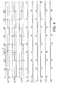
- the rectifier bridge 50 supplied with three-phase and its notch generator operation switching, are in themselves well known to humans of career. To facilitate understanding of the following of the presentation relating to the operation of the circuit shown in Figure 2, the cause of generation switch slots during operation of the deck 50 will be briefly recalled below.
- the reference voltage used to define in the following description, the phase angle and the period of the supply current is the voltage V RT between phases 11 and 13.
- the thyristors of bridge 50 are switched on cyclically in the following order: 51, 61, 52, 62, 53.63 by successive phase shift of 60 degrees one by compared to each other.
- Each thyristor has a duration of conduction corresponding to a third of the period from supply current: 120 ° electrical
- This angle is called the thyristor opening angle or commonly the rectifier control angle.
- the passages from a low level to a high level correspond to the instants of control of conduction of the different thyristors.
- the passages from a high level to a low level correspond to the instants of cessation of conduction of the thyristor.
- the curves shown in the different figures assume that the phases are balanced.
- the current flows during the first half of thyristor ignition period 51, from phase 11, point 24, through the thyristor 51, from charge 16 and returns in phase 12 to across thyristor 63.
- the thyristors 51 and 61 are on, the current flows from phase 11, point 24 through thyristor 51, from charge 16 and returns to phase 13 through the thyristor 61.
- the current circulates between a phase whose voltage is algebraically maximum and a phase whose voltage is algebraically minimum.
- the thyristor switches on and off do not are not instantaneous but are performed on a small duration, illustrated in FIG. 4 by the fact that the current value transitions take place on a short duration corresponding to a switching angle designated by ⁇ .
- ⁇ a switching angle designated by ⁇ .
- the instant the thyristor for example 52 receives a command ignition which marks the start of a current flow positive in phase 12 with a return marked by a negative current in phase 13, thyristor 51 arrives at the start of its short extinction period and is therefore not yet extinct. It follows that during the switching angle ⁇ , phases 11 and 12 are in short circuit through the anode connections of the thyristors 51 and 52.
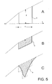
- Figure 5 part A represents the evolution the value of the voltage between phases during a angular duration including the switching angle.
- the short circuit between phases during switching results in a voltage drop between phases 11 and 12 marked in this figure by a notch b of angle ⁇ and of depth p, constituting what is called the switching notch.
- a switching notch resulting from a short circuit level of bridge 50 between two phases of the three-phase network feed the load 15.
- the width of the switch notch was markedly exaggerated for the sake of clarity of the figure.
- this notch As is known, the repercussion of this notch at the supply network, say upstream of points A, B, C located on each phases respectively of Figure 2, is attenuated by the presence of an inductor placed between the source 10, constituted for example by the connection on the network and the rectifier bridge 50.
- the attenuation of the depth of this notch results in a notch attenuated depth as shown in Figure 5 part B.
- the depth of this notch is proportional to the ratio L1 / L1 + L2.
- L1 report denotes the value of the inductance of the upstream network points A, B, C and L2 the value of the inductance added downstream of points A, B, C.
- the inductance L1 of the network has not been symbolized in Figure 2. This solution has the disadvantages explained more high.
- the inductors 21, 22, 23 each consist of a primary winding and a secondary winding magnetically coupled together, a means of switching provided with a control input allowing short circuit the secondary winding.
- the windings inductors are short circuited the most of the time.
- the inductances of these two short-circuit phases are put into service, by application to control inputs of the means of switching of the inductors of each of these phases in short circuit, of the second logic signal rendering non passing said switching means for the duration of commutation.
- the emission of the second logic signals of switching command of the switching means 17-19 is achieved by a synchronization means 30 of the on or off state of the switching means 17, 18, 19.
- the synchronization means 30 of the on state or not passing switching means 17, 18, 19 connected respectively in parallel on the windings secondary 47, 48, 49 of each inductor 21, 22, 23 of each phase 11, 12, 13 receives the control signal switching thyristors 51, 52, 53; 61, 62, 63.
- This control signal is received by links 74-76 connected to control inputs 64-66 respectively thyristors 61, 63, 62 and by links 94-96 connected to control inputs 54-56 respectively thyristors 51-53.
- Figure 2 so as not to overload the figure, it was only represented the link 74 between the synchronization means 30 and control input 64 of thyristor 61.
- Synchronization means 30 has outputs coupled by links 34-36 respectively to control inputs 84-86 of the switching means 17-19 respectively.
- links 34-36 respectively to control inputs 84-86 of the switching means 17-19 respectively.
- link 34 joining a output of the synchronization means 30 at the input of command 84 of switching means 17 has been represented. It must be understood, however, that the means synchronization 30 is linked by a link 35 to the control input 85 of the switching means 18 and by a link 36 to the command input 86 of the means switching 19.
- the second logic signal present on each outputs 34-36 of synchronization means 30 is as, as explained above, each of the switches 87-89 is mostly passing. However each time the first logic signal is received control switch for a thyristor on the bridge rectifier 50 on an input 74-76; 94-96 of circuit 30 the second logic signal will be issued. This second signal logic will be issued on two of the 34-36 links between the synchronization means 30 and a control input 84-86 switching means 17-19. This second logic signal has the effect of service during the short switching time both inductors which, depending on the thyristor of the bridge rectifier 50 put into conduction, are in short circuit. It is recalled that during the commissioning of a inductance 21-23 the switching means 17-19 of this inductance is non-conducting.
- This signal once modified will constitute the second logic signal.
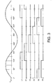
- the evolution over time of the second logic signal CK1 present at output 34 of the synchronization means 30, is shown in FIG. 4.
- This signal consists of a series of pulses. During each of these pulses, the switch 87 is non-conducting. We see that these pulses substantially coincide with the durations during which the derivative of the current I R in phase 11 is not zero.
- the synchronization means 30 must preferably receive the command moments from conduction of the thyristors received on link 74, the values of voltages between phases of the upstream network inductors 21-23, the values of the currents back in the phases.
- the circuit synchronization 30 has inputs 37-39 receiving a signal representative of the value of the phase current and inputs 74-76, 94-96 receiving a signal representative of the switching instants of rectifiers 51-53; 61-63, of the rectifier assembly 50.
- the circuit synchronization 30 has inputs 37-39 receiving a signal representative of the value of the phase current and inputs 41-43 receiving a representative signal the value of the voltage between phases.
- the circuit of synchronization 30 according to this embodiment may also have inputs 74-76, 94-96 receiving a signal representative of the switching instants of the rectifiers 51-53; 61-63, of the rectifier assembly 50.
- each of the circuits 27-29 is constituted as indicated above but the inductors 21-23 are saturable. More precisely their saturation level is chosen for that these inductances are saturated for a current of a low value compared to the maximum value that can take the rectified peak current in one rectifiers of the bridge 50.
- the inductors 21-23 are designed to present in the state saturated a leakage inductor in series with the inductance L1 of the network.
- the synchronization means 30 receives this command and sends through connections 34 35 of the second logic signals on the commands 84, 85 thus controlling the lifting of the short circuit secondary windings 47, 48 of inductors 21, 22 of phases 11 and 12.
- the inductors 21, 22 are thus put into service for the duration of switching.
- the switching times are materialized by the points o, o 'on curves 11 and 12 respectively representing the currents descending and ascending in phases 11 and 12.
- the current is at 0 in phase 12 and at a value nominal Id in phase 11.
- From point o inductance 22 of phase 12 begins a phase of saturation which ends at point a where this inductance is saturated. This is reflected in the fact that the current in phase 12 increases weakly during the saturation phase.
- the current Id in phase 11 decreases slightly until reaching the point a '.
- inductance 21 which was already saturated by the passage of the current Id remains saturated, so that the two inductors 21 and 22 are saturated.
- the current continues to increase in phase 12 and correspondingly decrease in phase 11 to the points shown in b and b 'respectively on curves 11 and 12.
- the current in inductance 21 of phase 11 flows to below the saturation threshold.
- Inductance 21 is desaturation according to the desaturation slope up to return to 0 at point c '.
- the decrease slope of the segment b'c 'on curve 11 is equal to the slope of the segment o'a '.
- the current increases so symmetrical in phase 11 according to segment bc up to reach its nominal value Id.
- the second signal logic takes a value making passing the means switching 17 and 18.
Landscapes
- Engineering & Computer Science (AREA)
- Power Engineering (AREA)
- Rectifiers (AREA)
- Dc-Dc Converters (AREA)
Abstract
Description
- la figure 1 représente un circuit électrique selon l'invention,
- la figure 2 représente un circuit d'alimentation d'une charge à partir d'un réseau triphasé dans lequel pour chaque phase, un enroulement primaire d'une inductance selon l'invention est inséré entre le réseau et un ensemble redresseur.
- la figure 3 représente un chronogramme des états passants des redresseurs d'un ensemble redresseur hexaphasé en conjonction avec une courbe représentant la valeur de la tension entre phases.
- la figure 4 représente des courbes de l'évolution dans le temps:
- de la valeur instantanée du courant dans chacune des trois phases au cours des cycles de commutation, (trois courbes supérieures)
- de la valeur absolue instantanée de la dérivée du courant dans chacune des trois phases au cours des cycles de commutation, (trois courbes centrales) et enfin,
- du second signal logique commandant l'état non passant de l'interrupteur de chacun des moyens de commutation d'inductances selon l'invention placées sur chacune des phases du réseau triphasé d'alimentation, (trois courbes inférieures).
- la figure 5 comporte les parties A, B, C. Chaque partie représente une forme d'encoche de commutation.
- la figure 6 est un détail agrandit de la figure 4 représentant l'évolution de la valeur du courant dans deux phases d'alimentation de l'ensemble redresseur pendant une commutation d'un redresseur de cet ensemble dans le cas où chacune de ces phases est chargée pendant ladite commutation par un circuit inductif saturable tel que représenté figure 1.
- α est l'angle de commande du redresseur,
- µ est l'angle de commutation
- Id est la valeur moyenne du courant de sortie du redresseur
- X est la valeur de la réactance série dans une
phase soit (L1 + L'2)
ω , L1 étant la valeur de l'inductance réseau, L'2, la valeur de l'inductance selon l'invention etω la pulsation du courant de la source 10, - V est la valeur efficace de la tension entre deux phases au niveau de l'ensemble redresseur.
Claims (9)
- Circuit électrique (20) comportant une inductance (2), l'inductance (2) comprenant un enroulement primaire (3) couplé magnétiquement à un enroulement secondaire (4) chargé par une résistance de charge (6) connectée en parallèle sur ledit enroulement secondaire (4), circuit caractérisé en ce qu'il comporte un moyen de commutation (1) ayant une entrée (81) de commande, connecté en parallèle sur l'enroulement secondaire (4), ledit moyen de commutation (1) étant capable de deux états, un état passant dans lequel l'enroulement secondaire (4) est court-circuité en sorte que la valeur de l'inductance (2) se trouve annulée et un état non passant dans lequel l'inductance (2) présente une valeur nominale souhaitée.
- Circuit (20) selon la revendication 1 caractérisé en ce que le moyen de commutation (1) comporte un moyen redresseur (7) double alternance placé parallèlement à l'enroulement secondaire (4).
- Circuit (20) selon la revendication 2, caractérisé en ce que le moyen de commutation (1) comporte une branche (14) connectée en parallèle sur l'enroulement secondaire (4), cette branche (14) portant un interrupteur (8) muni d'une entrée de commande (81), cette entrée de commande (81) de l'interrupteur (8) constituant l'entrée de commande du moyen de commutation (1) .
- Circuit (20) selon l'une des revendications 1 à 3, caractérisé en ce que l'inductance (2) est saturable.
- Circuit (100) d'alimentation d'une charge (16) à partir d'une source (10) polyphasée dans lequel chacune des phases (11, 12, 13) d'alimentation est connectée en série avec une branche (57-59) d'un ensemble redresseur (50) formé par un ensemble de redresseurs (51-53;61-63), chaque redresseur (51-53; 61-63) ayant une entrée de commande (54-56; 64-66) recevant un premier signal logique de commande, ledit premier signal logique commandant l'état passant desdits redresseurs (51-53; 61-63), circuit (100) d'alimentation d'une charge (16) caractérisé en ce qu'il comporte sur chacune des phases (11, 12, 13), un circuit (21-23) selon l'une des revendications 1 à 4, le moyen (17-19) de commutation de chaque circuit (21-23) selon l'une des revendications 1 à 4 étant passant ou non passant selon la valeur d'un second signal logique appliqué à son entrée de commande (84-86) de commutation, le second signal logique étant délivré par des moyens (30) de synchronisation et élaborant le second signal logique pour rendre non passant pendant la commutation d'un redresseur (51-53; 61-63), les moyens (17-19) de commutation de deux circuits (21-23) selon l'une des revendications 1 à 4.
- Circuit (100) selon la revendication 5 caractérisé en ce que le circuit de synchronisation (30) a des entrées (37-39) recevant un signal représentatif de la valeur du courant de phase et des entrées (74-76, 94-96) recevant un signal représentatif des instants de commutation des redresseurs (51-53; 61-63), de l'ensemble redresseur.
- Circuit (100) selon la revendication 6 caractérisé en ce que le circuit de synchronisation (30) a en outre des entrées (41-43) recevant un signal représentatif de la valeur de la tension entre phases.
- Circuit (100) selon la revendication 5 caractérisé en ce que le circuit de synchronisation (30) a des entrées (37-39) recevant un signal représentatif de la valeur du courant de phase et des entrées (41-43) recevant un signal représentatif de la valeur de la tension entre phases.
- Circuit (100) selon l'une des revendications 5 à 8 caractérisé en ce que la source (10) est une source triphasé et en ce que l'ensemble redresseur (50) est un pont redresseur hexaphasé.
Applications Claiming Priority (2)
| Application Number | Priority Date | Filing Date | Title |
|---|---|---|---|
| FR0110729 | 2001-08-10 | ||
| FR0110729A FR2828597B1 (fr) | 2001-08-10 | 2001-08-10 | Inductance a valeur commandable par commutation |
Publications (2)
| Publication Number | Publication Date |
|---|---|
| EP1283588A2 true EP1283588A2 (fr) | 2003-02-12 |
| EP1283588A3 EP1283588A3 (fr) | 2004-12-08 |
Family
ID=8866471
Family Applications (1)
| Application Number | Title | Priority Date | Filing Date |
|---|---|---|---|
| EP02291997A Withdrawn EP1283588A3 (fr) | 2001-08-10 | 2002-08-08 | Inductance à valeur commandable par commutation |
Country Status (2)
| Country | Link |
|---|---|
| EP (1) | EP1283588A3 (fr) |
| FR (1) | FR2828597B1 (fr) |
Citations (3)
| Publication number | Priority date | Publication date | Assignee | Title |
|---|---|---|---|---|
| US3845380A (en) * | 1972-05-22 | 1974-10-29 | V Lepp | Current stabilizer having a saturable reactor in the mode of forced magnetization |
| US4133018A (en) * | 1976-06-18 | 1979-01-02 | Hitachi, Ltd. | Thyristor fault-detecting apparatus |
| US6130832A (en) * | 1999-11-08 | 2000-10-10 | Otis Elevator Company | Active filtering of AC/DC switched converter input current |
-
2001
- 2001-08-10 FR FR0110729A patent/FR2828597B1/fr not_active Expired - Fee Related
-
2002
- 2002-08-08 EP EP02291997A patent/EP1283588A3/fr not_active Withdrawn
Patent Citations (3)
| Publication number | Priority date | Publication date | Assignee | Title |
|---|---|---|---|---|
| US3845380A (en) * | 1972-05-22 | 1974-10-29 | V Lepp | Current stabilizer having a saturable reactor in the mode of forced magnetization |
| US4133018A (en) * | 1976-06-18 | 1979-01-02 | Hitachi, Ltd. | Thyristor fault-detecting apparatus |
| US6130832A (en) * | 1999-11-08 | 2000-10-10 | Otis Elevator Company | Active filtering of AC/DC switched converter input current |
Non-Patent Citations (2)
| Title |
|---|
| SATO Y ET AL: "A CURRENT-TYPE PWM RECTIFIER WITH ACTIVE DAMPING FUNCTION" IEEE TRANSACTIONS ON INDUSTRY APPLICATIONS, IEEE INC. NEW YORK, US, vol. 32, no. 3, 1 mai 1996 (1996-05-01), pages 533-541, XP000598105 ISSN: 0093-9994 * |
| TANAKA T ET AL: "A new combined system of series active and shunt passive filters aiming at harmonic compensation for large capacity thyristor converters" PROCEEDINGS OF THE INTERNATIONAL CONFERENCE ON INDUSTRIAL ELECTRONICS,CONTROL AND INSTRUMENTATION (IECON). KOBE, OCT. 28 - NOV. 1, 1991, NES YORK, IEEE, US, vol. 1 CONF. 17, 28 octobre 1991 (1991-10-28), pages 723-728, XP010042068 ISBN: 0-87942-688-8 * |
Also Published As
| Publication number | Publication date |
|---|---|
| FR2828597A1 (fr) | 2003-02-14 |
| EP1283588A3 (fr) | 2004-12-08 |
| FR2828597B1 (fr) | 2003-11-07 |
Similar Documents
| Publication | Publication Date | Title |
|---|---|---|
| CA2059683C (fr) | Gradateur de courant pour charge de puissance, avec pertes de filtrage reduites | |
| FR2527889A1 (fr) | Procede et appareil de reduction des harmoniques dans les circuits ballasts de lampe a decharge dans les gaz | |
| FR2542555A1 (fr) | Circuit de commande pour lampes a decharge de gaz | |
| FR2479634A1 (fr) | Systeme de commande d'eclairage par lampes a decharge, permettant de reduire leur intensite lumineuse | |
| EP0926926A1 (fr) | Dispositif d'alimentation de plusieurs circuits résonants par un générateur de puissance à onduleur | |
| FR2733095A1 (fr) | Dispositif a inductance variable et utilisation de ce dispositif pour la realisation d'une source de courant pour cellule de commutation a tension nulle | |
| EP0788678B1 (fr) | Procede et dispositif de commande de puissance d'une charge via un systeme a reglage de phase | |
| FR2772154A1 (fr) | Circuit de commande pour la correction du facteur de puissance | |
| EP0623991B1 (fr) | Dispositif de commande de variation de puissance et/ou de vitesse d'une charge | |
| EP0986288B1 (fr) | Dispositif d'alimentation à onduleur dont la puissance délivrée est controlée | |
| FR2754655A1 (fr) | Interrupteur electronique a alimentation deux fils | |
| EP1283588A2 (fr) | Inductance à valeur commandable par commutation | |
| EP2781023B1 (fr) | Variateur de puissance | |
| FR2539563A1 (fr) | Source de puissance alternative haute frequence | |
| FR2717015A1 (fr) | Alimentation à découpage adaptée pour permettre des commutations sous tension réduite. | |
| FR2712763A1 (fr) | Générateur de courant ondulé à self saturable. | |
| EP0967842B1 (fr) | Emission d'une consigne de fonctionnement par une ligne d'alimentation alternative | |
| FR2627915A1 (fr) | Convertisseur de puissance de courant continu en courant continu | |
| EP0054445B1 (fr) | Dispositif électronique de chauffage à induction | |
| FR2803140A1 (fr) | Generateur analogique d'impulsions de tension | |
| FR2465361A1 (fr) | Circuit d'alimentation controle a courant continu a recuperation | |
| FR2555375A1 (fr) | Convertisseur continu-continu a inductance de charge commutee | |
| EP0614200B1 (fr) | Dispositif de limitation de la tension aux bornes d'un enroulement de transformateur | |
| FR2705856A1 (fr) | Système électrique de chauffage d'un pare-brise. | |
| EP0148085A1 (fr) | Dispositif de mise sous tension d'un circuit d'alimentation pour magnétron, notamment pour four à microonde |
Legal Events
| Date | Code | Title | Description |
|---|---|---|---|
| PUAI | Public reference made under article 153(3) epc to a published international application that has entered the european phase |
Free format text: ORIGINAL CODE: 0009012 |
|
| AK | Designated contracting states |
Designated state(s): AT BE BG CH CY CZ DE DK EE ES FI FR GB GR IE IT LI LU MC NL PT SE SK TR |
|
| AX | Request for extension of the european patent |
Extension state: AL LT LV MK RO SI |
|
| PUAL | Search report despatched |
Free format text: ORIGINAL CODE: 0009013 |
|
| AK | Designated contracting states |
Kind code of ref document: A3 Designated state(s): AT BE BG CH CY CZ DE DK EE ES FI FR GB GR IE IT LI LU MC NL PT SE SK TR |
|
| AX | Request for extension of the european patent |
Extension state: AL LT LV MK RO SI |
|
| AKX | Designation fees paid | ||
| REG | Reference to a national code |
Ref country code: DE Ref legal event code: 8566 |
|
| RAP1 | Party data changed (applicant data changed or rights of an application transferred) |
Owner name: ELECTRICITE DE FRANCE |
|
| STAA | Information on the status of an ep patent application or granted ep patent |
Free format text: STATUS: THE APPLICATION IS DEEMED TO BE WITHDRAWN |
|
| 18D | Application deemed to be withdrawn |
Effective date: 20050609 |