EP1282279A2 - Compensation of frequency offset in quadrature demodulators - Google Patents
Compensation of frequency offset in quadrature demodulators Download PDFInfo
- Publication number
- EP1282279A2 EP1282279A2 EP02017316A EP02017316A EP1282279A2 EP 1282279 A2 EP1282279 A2 EP 1282279A2 EP 02017316 A EP02017316 A EP 02017316A EP 02017316 A EP02017316 A EP 02017316A EP 1282279 A2 EP1282279 A2 EP 1282279A2
- Authority
- EP
- European Patent Office
- Prior art keywords
- phase
- output
- signal
- frequency
- quadrature
- Prior art date
- Legal status (The legal status is an assumption and is not a legal conclusion. Google has not performed a legal analysis and makes no representation as to the accuracy of the status listed.)
- Granted
Links
Images


Classifications
-
- H—ELECTRICITY
- H04—ELECTRIC COMMUNICATION TECHNIQUE
- H04L—TRANSMISSION OF DIGITAL INFORMATION, e.g. TELEGRAPHIC COMMUNICATION
- H04L27/00—Modulated-carrier systems
- H04L27/18—Phase-modulated carrier systems, i.e. using phase-shift keying
- H04L27/22—Demodulator circuits; Receiver circuits
- H04L27/227—Demodulator circuits; Receiver circuits using coherent demodulation
- H04L27/2271—Demodulator circuits; Receiver circuits using coherent demodulation wherein the carrier recovery circuit uses only the demodulated signals
- H04L27/2273—Demodulator circuits; Receiver circuits using coherent demodulation wherein the carrier recovery circuit uses only the demodulated signals associated with quadrature demodulation, e.g. Costas loop
-
- H—ELECTRICITY
- H04—ELECTRIC COMMUNICATION TECHNIQUE
- H04L—TRANSMISSION OF DIGITAL INFORMATION, e.g. TELEGRAPHIC COMMUNICATION
- H04L27/00—Modulated-carrier systems
- H04L27/18—Phase-modulated carrier systems, i.e. using phase-shift keying
- H04L27/22—Demodulator circuits; Receiver circuits
- H04L27/227—Demodulator circuits; Receiver circuits using coherent demodulation
- H04L27/2271—Demodulator circuits; Receiver circuits using coherent demodulation wherein the carrier recovery circuit uses only the demodulated signals
- H04L27/2272—Demodulator circuits; Receiver circuits using coherent demodulation wherein the carrier recovery circuit uses only the demodulated signals using phase locked loops
-
- H—ELECTRICITY
- H04—ELECTRIC COMMUNICATION TECHNIQUE
- H04L—TRANSMISSION OF DIGITAL INFORMATION, e.g. TELEGRAPHIC COMMUNICATION
- H04L27/00—Modulated-carrier systems
- H04L27/32—Carrier systems characterised by combinations of two or more of the types covered by groups H04L27/02, H04L27/10, H04L27/18 or H04L27/26
- H04L27/34—Amplitude- and phase-modulated carrier systems, e.g. quadrature-amplitude modulated carrier systems
- H04L27/38—Demodulator circuits; Receiver circuits
- H04L27/3845—Demodulator circuits; Receiver circuits using non - coherent demodulation, i.e. not using a phase synchronous carrier
- H04L27/3854—Demodulator circuits; Receiver circuits using non - coherent demodulation, i.e. not using a phase synchronous carrier using a non - coherent carrier, including systems with baseband correction for phase or frequency offset
- H04L27/3872—Compensation for phase rotation in the demodulated signal
-
- H—ELECTRICITY
- H04—ELECTRIC COMMUNICATION TECHNIQUE
- H04L—TRANSMISSION OF DIGITAL INFORMATION, e.g. TELEGRAPHIC COMMUNICATION
- H04L27/00—Modulated-carrier systems
- H04L27/0014—Carrier regulation
- H04L2027/0024—Carrier regulation at the receiver end
- H04L2027/0026—Correction of carrier offset
- H04L2027/003—Correction of carrier offset at baseband only
-
- H—ELECTRICITY
- H04—ELECTRIC COMMUNICATION TECHNIQUE
- H04L—TRANSMISSION OF DIGITAL INFORMATION, e.g. TELEGRAPHIC COMMUNICATION
- H04L27/00—Modulated-carrier systems
- H04L27/0014—Carrier regulation
- H04L2027/0044—Control loops for carrier regulation
- H04L2027/0053—Closed loops
- H04L2027/0057—Closed loops quadrature phase
Definitions
- the present invention relates to a quadrature demodulator used for a digital radio communication system and the like.
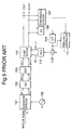
- Fig. 9 is a block diagram showing a conventional quadrature demodulator.
- reference numeral 101 denotes aquadrature detector
- reference numeral 102 denotes an oscillator.
- An input signal that has been subjected to a quadrature modulation that is, an input intermediate frequency signal (hereinafter referred to as an input IF signal)
- an input IF signal an input intermediate frequency signal
- Two outputs from the quadrature detector 101 are respectively converted to digital signals Ich3 and Qch3 by an A/D converter 103, and then output to an ROF (roll-off filter) 105.
- the signals which have been transmitted through the ROF 105 are output to a phase-rotator 104.
- phase-rotator 104 a PD (phase error detector) 108, a LPF (loop filter) 109, an adder 112 and a NCO (numerically controlled oscillator) 110 constitute a PLL (phase locked loop).
- a signal indicating an asynchronous state is output from a synchronization detector 107 to a frequency controller 111.
- the frequency controller 111 In the asynchronous state, the frequency controller 111 outputs a frequency signal such as a triangular wave to the adder 112.
- the adder 112 adds the output of the frequency controller 111 to the output of the LPF 109, and outputs the results to the NCO 110.
- the NCO 110 outputs sinusoidal signals (Sin ⁇ t and cos ⁇ t) to the phase-rotator 104, and said sinusoidal signals change their frequencies in accordance with the signal input to the NCO 110.
- the phase-rotator 104 performs a complex multiplication by use of the output of the ROF 105 and the output of the NCO 110, and performs a phase rotation so as to correct the phase shift between the input IF signal and the output of the oscillator 102.
- the value of the output of the frequency controller 111 at that time is kept, and the output of the frequency controller 111 is supplied to the NCO 110 via the adder 112.
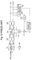
- the ROF 105 is arranged on the output side of the phase-rotator 104 as shown in Fig. 10.
- the ROF 105 is arranged in the PLL composed of the phase-rotator 104, the PD 108, the LPF 109, the adder 112 and the NCO 110.
- a digital filter is usually used as the ROF 105. Since a delay exists between a signal input of the ROF 105 and a signal output of the ROF 105, this PLL has a larger delay than the PLL in the demodulator of Fig. 9, therefore noises caused by the loop itself becomes much, and deteriorates the error rate characteristic. If a noise band width of the loop was narrowed in order to suppress the noises in the loop itself, a deterioration of the error rate characteristic would be essentially inevitable due to phase noises of the oscillator 102 and the like.
- An object of the present invention is to provide a quadrature demodulator which is capable of preventing deterioration of characteristics such as a bit error rate even when a shift between a frequency of an input IF signal and a frequency of an oscillator is large.
- a quadrature demodulator of the present invention comprises an oscillator for generating a signal having a predetermined frequency; a quadrature detector for converting an input IF signal to a base band signal by inputting the input IF signal and a signal of the oscillator; a roll-off filter having a predetermined pass band characteristic for shaping the base band signal; and a first phase rotator for performing a phase rotation so as to cancel a frequency shift between the frequency of the oscillator and a frequency of the input IF signal by inputting the base band signal which has transmitted through the roll-off filter, wherein a second phase rotator is provided at a former stage of the roll-off filter, and the base band signal transmits through a pass band of the roll-off filter by a phase rotation operation of the second phase rotator.
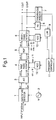
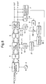
- Fig. 1 is a block diagram showing a first embodiment of a quadrature demodulator according to the present invention.
- an input signal in this embodiment is an output signal of a quadrature demodulation system such as a QAM (quadrature amplitude modulation) modulator.
- reference numeral 1 denotes a quadrature detector
- reference numeral 2 denotes an oscillator which generates a signal of a predetermined frequency (reference carrier wave).
- the quadrature-modulated input signal (an input IF signal) is input to the quadrature detector 1, and the quadrature detector 1 multiplies the IF signal with the signal of the oscillator 2 for converting the multiplied signal to a base band signal.
- a first phase rotator 4 is provided at the front stage of a ROF (roll-off filter) 5 as described later.
- a coarse adjustment of the frequency shift which is performed in the first phase rotator 4 if there is a large shift between the frequency fc of the input IF signal and the frequency fc' of the oscillator 2, the base band signal passes through the pass band of the roll-off filter 5.
- two quadrature components of the base band signal shall be denoted as Ich and Qch.
- the method of the detection is a quasi-synchronous detection. Therefore, an output signal of the oscillator 2 (reference carrier wave) is not synchronized with the carrier wave of the input IF signal.
- An A/D converter 3 converts analog signals Ich1 and Qch1 to digital signals Ich2 and Qch2 for performing subsequent process digitally.
- a NCO (numerically controlled oscillator) 12 is a sinusoidal oscillator for generating a sinusoidal signal which changes its frequency in accordance with a magnitude of an output signal of a frequency controller 11 as described later. Then, the frequency controller 11 is controlled based on an output of a second phase rotator 6 via a synchronous detector 7 as described later.
- a phase rotation of the first phase rotator 4 is controlled by the above-mentioned loop (first loop) which a loop from the second phase rotator 6 to an output terminal of the NCO 12.
- the NCO 12 outputs signals having phases different by ⁇ /2, which correspond to sin ⁇ t and cos ⁇ t.
- the quasi-synchronous detection is not limited to the above-described method.
- a method in which a quadrature detection is digitally performed after performing the A/D conversion to the input IF signal can be applied to the present invention.
- the first phase rotator 4 is connected to the A/D converter 3 and the NCO 12, and input signals (Ich2, Qch2) from the A/D converter 3 and signals (cos ⁇ t, sin ⁇ t) from the NCO 12.
- they are regarded as complex number like Ich2 + jQch2 and cos ⁇ t + jstn ⁇ t , and performed a complex multiplication .
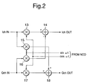
- the first phase rotation 4 includes multipliers, 13, 15, 16 and 17 and adders 14 and 18, and performs the multiplications by use of the signals (Ich2, Qch2) which are input from the A/D converter 3 and the signals (cos ⁇ t, sin ⁇ t) which are input from the NCO 12, which are expressed by the following equations.
- Ich3 Ich2 ⁇ cos ⁇ t + Qch2 ⁇ sin ⁇ t
- Qch3 Ich2 ⁇ sin ⁇ t - Qch2 ⁇ cos ⁇ t
- the ROF 5 is a roll-off filter which performs waveform shaping on a receiving side.
- This filter is constituted by a digital filter, and there are various constitutions of the filter. Since the digital filter has been known widely, detailed descriptions are omitted herein. Note that in the digital filter, in accordance with the number of taps a delay occurs between the input of the signal and the output thereof.
- the second phase rotator 6 has the same constitution as that of the first phase rotator 4, and performs a complex multiplication of Ich4 and Qch4 that are the output of the ROF5 with sin ⁇ t and cos ⁇ t that are the output of the NCO (numerically controlled oscillator) 10. This complex multiplication is performed based on the equations (1) and (2).
- the synchronous detector 7 is a circuit which detects whether the carrier synchronization is established, and any method can be used as long as the detector 7 is capable of detecting the carrier synchronization.
- the synchronous detector 7 outputs "1" when the detector 7 detects that the carrier synchronization is established, and outputs "0" when the detector 7 decides that the carrier synchronization is not established.
- the PD (phase error detector) 8 detects the phase error of the demodulated signal, and may be capable of simply detecting whether the phase advances or delays.
- the PD 8 may operate in such a manner that if the phase advances as shown in Fig. 3, the PD 8 outputs "+1" and, if the phase delays, the PD outputs "-1".
- the PD 8 may output a continuous output in accordance with the magnitudes of the advance and delay of the phase.
- the LPF 9 is a loop filter for removing high frequency components of the phase error signal output from the PD 8.
- the NCO (numerically controlled oscillator) 10 is an oscillator for generating a sinusoidal signal which changes its frequency in accordance with the magnitude of the phase error signal output from the LPF 9.
- the output of the LPF 9 is controlled based on the output of the second phase rotator 6 via the PD 8.
- the phase rotation of the second phase rotator 6 is controlled by the above-mentioned loop (second loop) which is a loop from the second phase rotator 6 to the output of the NCO 10.
- there are two outputs of the NCO 10 and these correspond to sin ⁇ t and cos ⁇ t, which differs from each other in their phases by ⁇ /2.
- the NCO 10 has quite the same constitution as that of the NCO 12, and descriptions are omitted.
- the frequency controller 11 outputs frequency waveforms such as triangle waves and sinusoidal waves when the carrier is in an asynchronous state.
- the frequency controller 11 adjusts its output so that the output of the LPF 9 is smaller than a setting value when the carrier is in a synchronous state.
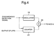
- Fig. 4 is a block diagram showing an example of the frequency controller 11.
- the frequency controller 11 includes an oscillator 19, a counter 21 and an adder 20.
- the oscillator 19 outputs a periodic waveform signal when it is detected that the input from the synchronous detector 7 is "0", that is, when it is detected that the carrier is in the asynchronous state.
- the periodic waveform signal from the oscillator 19 is a periodic waveform signal such as sinusoidal wave signal and triangular wave signal.
- the oscillator 8 outputs sinusoidal wave signal. It is possible to change the cycle of the periodic waveform signal and the amplitude thereof by setting them.
- the oscillator 19 fixes its operation and holds the final value of its output.
- the counter 21 is constituted by an up and down counter.
- the counter 21 When the carrier is in the asynchronous state, the counter 21 is reset. And when it is decided that the carrier is in the synchronous state, the counter 21 increases and decreases its count number in accordance with the polarity of the output of the LPF 9 if the output of the LPF 9 exceeds the predetermined setting range. The operation of the counter 21 is continued until the output of the LPF 9 falls within the setting range.
- the outputs of the oscillator 19 and the counter 21 are added to each other by the adder 20, and the output of the adder 20 is output to the NCO 12.
- the input IF signal is converted to two quadrature components Ich1 and Qch1 by the oscillator 2 and the quadrature detector 1.
- the quadrature demodulator of Fig. 1 adopts a type of a quasi-synchronous demodulator, the carrier wave of the input IF signal and the output of the oscillator 2 are not synchronized with each other.
- the signal point appearing on the I-Q plane by the two quadrature components Ich1 and Qch1 after the detection rotates in accordance with a difference between the frequency of the carrier wave of the IF signal and the frequency of the oscillator 2.
- a QPSK system is adopted in Fig. 5.
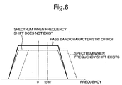
- the spectrum of Ich1 and Qch1 shifts from the original position by the difference between the carrier wave frequency f of the input IF signal and the output frequency f' of the oscillator 2.
- the first phase rotator 4 performs the complex multiplication as described above. Then, the base band signal whose central frequency is swept by the first phase rotator 4 transmits through the ROF 5, and is input to the second phase rotator 6. Specifically, since the base band signal always transmits through the pass band of the ROF 5 by the sweeping operation, the base band signal is input to the a carrier recovery PLL circuit including the second phase rotator 6, the PD 8, the LPF 9 and the NCO 10. In the carrier recovery PLL, the phase error detected by the PD 8 transmits through the LPF 9, and is output to the NCO 10. And the NCO 10 outputs a sinusoidal signal which changes its frequency in accordance with the magnitude of the phase error. By performing the complex multiplication similarly to the first phase rotator 4, the second phase rotator 6 performs the phase rotation so as to cancel the phase shift between the input IF signal and the output of the oscillator 2.
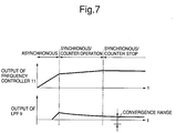
- Fig. 7 shows an example of the outputs of the LPF 9 and the frequency controller 11 from the asynchronous state to the synchronous state.
- the periodic waveform signal is output from the oscillator 19 of the frequency controller 11.
- the case where the synchronous state is brought about at the leading edge of the triangular wave is shown, therefore only a part of the triangular wave is shown.
- the counter 21 of the frequency controller 11 continues to perform the up and down count operations until the output of the LPF 9 falls within the convergence range.
- the first phase rotator 4 is provided at the front stage of the ROF 5, and the central frequency of the base band signal is swept by the first phase rotator 4, so the base band signal is allowed to transmit through the pass band of the ROF 5. Accordingly, it is possible to correct the frequency shift at the front stage of the ROF 5 even if the spectrum of the base band signal shifts by the frequency shift of the oscillator 2. As a result, even if the difference between the frequency of the input IF signal and the frequency of the oscillator 2 is large, deterioration of the bit error rate characteristic can be prevented without attenuating a necessary signal uselessly.
- the frequency error is automatically detected and corrected, evenif the frequency changes due to the changes of temperature and humidity and the like, the frequency change does not affect the characteristics of the quadrature demodulator. Moreover, since the correction of the frequency shift is performed by the digital processing, integration of the quadrature demodulator is possible.
- Fig. 8 is a block diagram showing a second embodiment of the quadrature demodulator according to the present invention.
- the identical constituent components to those in Fig. 1 are denoted by the same reference numerals, and descriptions for them are omitted.
- the oscillator 19 and the counter 21, which are the constituent components of the frequency controller 11 in Fig. 1 are connected to each other via a controller 32, and the output of the oscillator 19 and the output of the LPF 9 are added by the adder 34. The result of the addition is output to the NCO 10, and the output of the counter 21 is output to the NCO 12.
- the controller 32 is a control circuit for controlling the oscillator 19 and the counter 21.
- Other constitutions are identical to those of Fig. 1.
- the controller 32 controls the oscillator 19 and the counter 21 so that the oscillator 19 outputs the periodic waveform signal and the counter 21 is reset.
- the oscillator 19 outputs the periodic waveform signal such as a triangular wave and the like, similarly to the first embodiment.
- the counter 21 is in a reset state
- the first phase rotator 4 is in a nonoperative state
- the first phase rotator 4 is in a state where the first phase rotator 4, that is, the input signal is output as it is.
- the spectrum of the input base band signal of the second phase rotator 6 is swept by a frequency determined by an amplitude of an output of the oscillator 9.
- the controller 32 stops the operation of the oscillator 19, and starts an operation to move the last output value of the oscillator 19 at that time to the counter 21.
- the output of the oscillator 19 is made tobe gradually close to zero, and the output of the counter 21 is made to be gradually close to the final value of the oscillator 19.
- the central frequency of the base band signal is coincident with the center of the pass band characteristic of the ROF 5, and the base band signal comes to transmit through the pass band of the ROF 5.
- the output of the LPF 9 is subsequently monitored. If the output of the LPF 9 has a magnitude exceeding the predetermined setting range, the counter 21 performs either a count-up operation or a count-down operation depending on the polarity of the LPF 9, and the counter 21 operates until the output of the LPF 9 falls within the setting range.
- the adjustment of the frequency shift is previously performed by the second phase rotator 6, and the output of the oscillator 19 is made to be zero after the establishment of the carrier synchronization, and the final value of the oscillator 19 is transferred to the counter 21.
- the base band signal transmits through the pass band of the ROF 5 similarly to the first embodiment. Accordingly, in this embodiment, even if the spectrum of the base band signal shifts owing to the frequency shift of the oscillator 2, its correction is possible similarly to the first embodiment. Even if the difference between the frequency of the input IF signal and the frequency of the oscillator 2 is large, deterioration of the bit error rate characteristic can be prevented.
- an equalizer and the like may be provided at the rear stage of the second phase rotator 2. Such an equalizer never produces an evil effect on the operations of the present invention.
- the phase rotator is provided at the front stage of the roll-off filter, and the phase rotation operation of the phase rotator allows the base band signal to transmit through the pass band of the roll-off filter. Therefore, the frequency shift can be corrected even if the spectrum of the base band signal is shifted by the frequency shift of the oscillator. Deterioration of the bit error rate characteristic can be prevented even if the difference between the frequency of the input IF signal and the frequency of the oscillator is large.
Landscapes
- Engineering & Computer Science (AREA)
- Computer Networks & Wireless Communication (AREA)
- Signal Processing (AREA)
- Digital Transmission Methods That Use Modulated Carrier Waves (AREA)
- Superheterodyne Receivers (AREA)
Abstract
Description
Claims (12)
- A quadrature demodulator, comprising:a quasi-synchronous detector for performing a quasi-synchronous detection for a quadrature-modulated input signal;a first phase rotator for phase-rotating an output of the quasi-synchronous detector;a roll-off filter for performing waveform shaping on an output of the first phase rotator;a second phase rotator for phase-rotating an output of the roll-off filter;a first loop for controlling a phase rotation of the first phase rotator based on an output of the second phase rotator; anda second loop for controlling a phase rotation of the second phase rotator.
- The quadrature demodulator according to claim 1, wherein the first loop controls an output of the quadrature detector by a phase rotation of the first phase rotator so that the output of the quadrature detector transmits through a pass band of the roll-off filter.
- The quadrature demodulator according to claim 1 or 2, wherein the second loop cancels a frequency difference of a reference carrier wave of the quadrature synchronous detector and a carrier wave of an input signal by a phase rotation of the second phase rotator.
- The quadrature demodulator according to one of the preceding claims, wherein the first phase rotator receives a signal which changes its frequency by a frequency range in accordance with an amplitude of a periodic waveform signal in a state where a carrier synchronization is not established, and sweeps a central frequency of the output of the quasi-synchronous detector, thus allowing the output of the quasi-synchronous detector to transmit through a pass band of the roll-off filter.
- The quadrature demodulator according to claim 4, wherein the amplitude of the periodic waveform signal holds its final value when the carrier synchronization is established.
- The quadrature demodulator according to claim 4 or 5, wherein in a case where a phase error between a reference carrier wave of the quasi-synchronous detector and a carrier wave of the input signal is out of a predetermined range when the carrier synchronization is established, the phase error is corrected by the amplitude of the periodic waveform signal so that the phase error is held within a predetermined range.
- A method for quadrature-demodulating, comprising the steps of:detecting a quadrature-modulated signal quasi-synchronously;first phase-rotating an output of said detecting step;filtering an output of said first phase-rotating step;second phase-rotating an output of said filtering step;first controlling said first phase-rotating step based on an output of said second phase-rotating step; andsecond controlling said second phase-rotating step.
- The method of claim 7, wherein said first controlling step controls an output of said detecting step by a phase rotation so that the output of said detecting step transmits through a pass band of the roll-off filter.
- The method of claim 7 or 8, wherein said second controlling step cancels a frequency difference of a reference carrier wave of said detecting step and a carrier wave of an input signal by a phase rotation of said second phase-rotating step.
- The method of claim one of the claims 7 to 9, wherein said first phase-rotating step receives a signal which changes its frequency by a frequency range in accordance with an amplitude of a periodic waveform signal in a state where a carrier synchronization is not established, and sweeps a central frequency of the output of said detecting step, thus allowing the output of said detecting step to transmit through a pass band of the roll-off filter.
- The method of claim 10, wherein said first controlling step holds the final value of the amplitude of the periodic waveform signal when the carrier synchronization is established.
- The method of claims 10 or 11, wherein in a case where a phase error between a reference carrier wave of said detecting step and a carrier wave of the input signal is out of a predetermined range when the carrier synchronization is established, said first controlling step corrects the phase error by the amplitude of the periodic waveform signal so that the phase error is held within a predetermined range.
Applications Claiming Priority (2)
| Application Number | Priority Date | Filing Date | Title |
|---|---|---|---|
| JP2001236523A JP2003046587A (en) | 2001-08-03 | 2001-08-03 | Demodulator |
| JP2001236523 | 2001-08-03 |
Publications (3)
| Publication Number | Publication Date |
|---|---|
| EP1282279A2 true EP1282279A2 (en) | 2003-02-05 |
| EP1282279A3 EP1282279A3 (en) | 2006-08-23 |
| EP1282279B1 EP1282279B1 (en) | 2014-10-08 |
Family
ID=19067773
Family Applications (1)
| Application Number | Title | Priority Date | Filing Date |
|---|---|---|---|
| EP02017316.7A Expired - Lifetime EP1282279B1 (en) | 2001-08-03 | 2002-08-01 | Compensation of frequency offset in quadrature demodulators |
Country Status (3)
| Country | Link |
|---|---|
| US (1) | US7133469B2 (en) |
| EP (1) | EP1282279B1 (en) |
| JP (1) | JP2003046587A (en) |
Cited By (4)
| Publication number | Priority date | Publication date | Assignee | Title |
|---|---|---|---|---|
| EP1458088A1 (en) * | 2003-03-13 | 2004-09-15 | Samsung Electronics Co., Ltd. | Apparatus for compensating the frequency offset in a receiver, and method |
| US6859648B2 (en) * | 2002-04-10 | 2005-02-22 | Kabushiki Kaisha Toshiba | Semiconductor integrated circuit device |
| WO2005086351A1 (en) * | 2004-03-02 | 2005-09-15 | International Business Machines Corporation | Providing automatic adaptation to frequency offsets in high speed serial links |
| CN104488241A (en) * | 2013-06-19 | 2015-04-01 | 华为技术有限公司 | Method and device for transmitting and receiving data |
Families Citing this family (10)
| Publication number | Priority date | Publication date | Assignee | Title |
|---|---|---|---|---|
| US7369606B1 (en) * | 2004-02-19 | 2008-05-06 | L-3 Communications Corporation | Phase error detector using I/Q interference cancellation |
| DE102004047424A1 (en) * | 2004-09-28 | 2006-04-06 | Micronas Gmbh | Circuit and method for carrier recovery |
| JP2006237819A (en) * | 2005-02-23 | 2006-09-07 | Nec Corp | Demodulator and phase compensation method therefor |
| US8502920B2 (en) | 2007-03-14 | 2013-08-06 | Vyacheslav Shyshkin | Method and apparatus for extracting a desired television signal from a wideband IF input |
| US8902365B2 (en) * | 2007-03-14 | 2014-12-02 | Lance Greggain | Interference avoidance in a television receiver |
| JP5046114B2 (en) * | 2007-12-12 | 2012-10-10 | 日本電気株式会社 | Multilevel QAM demodulator, demodulating method thereof, and radio communication system |
| FR2969426B1 (en) * | 2010-12-15 | 2013-08-30 | St Microelectronics Sa | CIRCUIT DEPHASAGE |
| US8891687B1 (en) * | 2013-06-26 | 2014-11-18 | Topcon Positioning Systems, Inc. | Digital system and method of estimating non-energy parameters of signal carrier |
| JP7547010B2 (en) * | 2020-08-31 | 2024-09-09 | 日本無線株式会社 | Carrier recovery circuit |
| WO2022172660A1 (en) * | 2021-02-15 | 2022-08-18 | 古野電気株式会社 | Demodulator and demodulation method |
Family Cites Families (13)
| Publication number | Priority date | Publication date | Assignee | Title |
|---|---|---|---|---|
| DE3765947D1 (en) * | 1986-01-18 | 1990-12-13 | Hewlett Packard Ltd | NON-INFLUENCY ANALYZER FOR DETECTING CHANNEL FAULTS. |
| JPH0658794A (en) | 1992-08-11 | 1994-03-04 | Sony Corp | Liquid level gage |
| JPH07297872A (en) | 1994-04-28 | 1995-11-10 | Matsushita Electric Ind Co Ltd | Demodulator |
| JPH08274832A (en) | 1995-03-31 | 1996-10-18 | Matsushita Electric Ind Co Ltd | Demodulator |
| JP3728573B2 (en) * | 1997-05-02 | 2005-12-21 | 富士通株式会社 | Demodulator |
| JP3663565B2 (en) * | 1997-11-10 | 2005-06-22 | 富士通株式会社 | Carrier recovery circuit |
| JPH11284677A (en) * | 1998-03-27 | 1999-10-15 | Nec Corp | Demodulator and digital radio communication system using it |
| JP3206553B2 (en) | 1998-07-22 | 2001-09-10 | 日本電気株式会社 | Demodulator |
| US6222891B1 (en) * | 1998-11-03 | 2001-04-24 | Broadcom Corporation | Timing recovery using the pilot signal in high definition TV |
| US6151368A (en) * | 1999-03-22 | 2000-11-21 | Sicom, Inc. | Phase-noise compensated digital communication receiver and method therefor |
| JP3634187B2 (en) * | 1999-04-23 | 2005-03-30 | 株式会社ケンウッド | BS digital broadcast receiver. |
| JP2001024724A (en) | 1999-07-08 | 2001-01-26 | Hitachi Denshi Ltd | Delay detection demodulator |
| US6624691B1 (en) * | 1999-10-04 | 2003-09-23 | Nec Corporation | Demodulator for processing digital signal |
-
2001
- 2001-08-03 JP JP2001236523A patent/JP2003046587A/en active Pending
-
2002
- 2002-08-01 US US10/208,841 patent/US7133469B2/en not_active Expired - Lifetime
- 2002-08-01 EP EP02017316.7A patent/EP1282279B1/en not_active Expired - Lifetime
Cited By (6)
| Publication number | Priority date | Publication date | Assignee | Title |
|---|---|---|---|---|
| US6859648B2 (en) * | 2002-04-10 | 2005-02-22 | Kabushiki Kaisha Toshiba | Semiconductor integrated circuit device |
| EP1458088A1 (en) * | 2003-03-13 | 2004-09-15 | Samsung Electronics Co., Ltd. | Apparatus for compensating the frequency offset in a receiver, and method |
| WO2005086351A1 (en) * | 2004-03-02 | 2005-09-15 | International Business Machines Corporation | Providing automatic adaptation to frequency offsets in high speed serial links |
| US7477713B2 (en) | 2004-03-02 | 2009-01-13 | International Business Machines Corporation | method for providing automatic adaptation to frequency offsets in high speed serial links |
| CN104488241A (en) * | 2013-06-19 | 2015-04-01 | 华为技术有限公司 | Method and device for transmitting and receiving data |
| CN104488241B (en) * | 2013-06-19 | 2018-09-21 | 华为技术有限公司 | Data sending, receiving method, terminal device and base station |
Also Published As
| Publication number | Publication date |
|---|---|
| EP1282279A3 (en) | 2006-08-23 |
| JP2003046587A (en) | 2003-02-14 |
| EP1282279B1 (en) | 2014-10-08 |
| US20030026358A1 (en) | 2003-02-06 |
| US7133469B2 (en) | 2006-11-07 |
Similar Documents
| Publication | Publication Date | Title |
|---|---|---|
| JP3616706B2 (en) | Demodulator with cross-polarization interference compensation function | |
| US7133469B2 (en) | Quadrature demodulator | |
| US20040066861A1 (en) | Quadrature demodulator for compensating for gain and phase imbalances between in-phase and quadrature-phase components | |
| CN101897163B (en) | Wireless communication device and dc offset adjustment method | |
| US4943982A (en) | Baseband carrier phase corrector | |
| US6191649B1 (en) | Quadrature demodulator and method for quadrature demodulation | |
| US5200977A (en) | Terminal unit apparatus for time division multiplexing access communications system | |
| RU2308815C1 (en) | Demodulator and phase compensation method for it | |
| JPH02100545A (en) | Demodulator | |
| JP3206553B2 (en) | Demodulator | |
| US7577219B2 (en) | Apparatus for communications | |
| US8457189B2 (en) | Receiving apparatus having equalizer, and receiving method | |
| JP2006121677A (en) | Circuit and method for regenerating carrier | |
| JPH0974431A (en) | Carrier phase synchronization circuit | |
| JP3504800B2 (en) | Quadrature demodulator | |
| JP2002374133A (en) | Automatic gain control circuit and automatic gain control method | |
| JP3518499B2 (en) | Demodulator | |
| US5790600A (en) | Method of compensating differences in group propagation times between the analog filters of a transmitter and between those of a receiver for signals in phase quadrature corresponding compensation apparatus and a corresponding transmission system | |
| JP3449341B2 (en) | Demodulator | |
| JP3206581B2 (en) | Demodulator | |
| JP2000244592A (en) | Demodulator | |
| JP4438581B2 (en) | Demodulator and demodulation method | |
| JP4375032B2 (en) | QAM transmission system and QAM receiver | |
| JP2827875B2 (en) | Microwave band signal generator | |
| JP2000236361A (en) | Wireless device and signal degradation compensation method |
Legal Events
| Date | Code | Title | Description |
|---|---|---|---|
| PUAI | Public reference made under article 153(3) epc to a published international application that has entered the european phase |
Free format text: ORIGINAL CODE: 0009012 |
|
| AK | Designated contracting states |
Designated state(s): AT BE BG CH CY CZ DE DK EE ES FI FR GB GR IE IT LI LU MC NL PT SE SK TR |
|
| AX | Request for extension of the european patent |
Extension state: AL LT LV MK RO SI |
|
| PUAL | Search report despatched |
Free format text: ORIGINAL CODE: 0009013 |
|
| RIC1 | Information provided on ipc code assigned before grant |
Ipc: H04L 27/227 20060101ALI20060707BHEP Ipc: H04L 27/38 20060101AFI20021111BHEP |
|
| AK | Designated contracting states |
Kind code of ref document: A3 Designated state(s): AT BE BG CH CY CZ DE DK EE ES FI FR GB GR IE IT LI LU MC NL PT SE SK TR |
|
| AX | Request for extension of the european patent |
Extension state: AL LT LV MK RO SI |
|
| 17P | Request for examination filed |
Effective date: 20061219 |
|
| AKX | Designation fees paid |
Designated state(s): DE FR GB IT |
|
| 17Q | First examination report despatched |
Effective date: 20110621 |
|
| GRAP | Despatch of communication of intention to grant a patent |
Free format text: ORIGINAL CODE: EPIDOSNIGR1 |
|
| INTG | Intention to grant announced |
Effective date: 20140416 |
|
| GRAS | Grant fee paid |
Free format text: ORIGINAL CODE: EPIDOSNIGR3 |
|
| GRAA | (expected) grant |
Free format text: ORIGINAL CODE: 0009210 |
|
| AK | Designated contracting states |
Kind code of ref document: B1 Designated state(s): DE FR GB IT |
|
| REG | Reference to a national code |
Ref country code: GB Ref legal event code: FG4D |
|
| REG | Reference to a national code |
Ref country code: DE Ref legal event code: R096 Ref document number: 60246677 Country of ref document: DE Effective date: 20141120 |
|
| REG | Reference to a national code |
Ref country code: DE Ref legal event code: R097 Ref document number: 60246677 Country of ref document: DE |
|
| PLBE | No opposition filed within time limit |
Free format text: ORIGINAL CODE: 0009261 |
|
| STAA | Information on the status of an ep patent application or granted ep patent |
Free format text: STATUS: NO OPPOSITION FILED WITHIN TIME LIMIT |
|
| 26N | No opposition filed |
Effective date: 20150709 |
|
| REG | Reference to a national code |
Ref country code: FR Ref legal event code: PLFP Year of fee payment: 15 |
|
| REG | Reference to a national code |
Ref country code: FR Ref legal event code: PLFP Year of fee payment: 16 |
|
| REG | Reference to a national code |
Ref country code: FR Ref legal event code: PLFP Year of fee payment: 17 |
|
| PGFP | Annual fee paid to national office [announced via postgrant information from national office to epo] |
Ref country code: FR Payment date: 20180712 Year of fee payment: 17 Ref country code: DE Payment date: 20180717 Year of fee payment: 17 Ref country code: IT Payment date: 20180823 Year of fee payment: 17 |
|
| PGFP | Annual fee paid to national office [announced via postgrant information from national office to epo] |
Ref country code: GB Payment date: 20180801 Year of fee payment: 17 |
|
| REG | Reference to a national code |
Ref country code: DE Ref legal event code: R119 Ref document number: 60246677 Country of ref document: DE |
|
| GBPC | Gb: european patent ceased through non-payment of renewal fee |
Effective date: 20190801 |
|
| PG25 | Lapsed in a contracting state [announced via postgrant information from national office to epo] |
Ref country code: DE Free format text: LAPSE BECAUSE OF NON-PAYMENT OF DUE FEES Effective date: 20200303 Ref country code: FR Free format text: LAPSE BECAUSE OF NON-PAYMENT OF DUE FEES Effective date: 20190831 |
|
| PG25 | Lapsed in a contracting state [announced via postgrant information from national office to epo] |
Ref country code: IT Free format text: LAPSE BECAUSE OF NON-PAYMENT OF DUE FEES Effective date: 20190801 Ref country code: GB Free format text: LAPSE BECAUSE OF NON-PAYMENT OF DUE FEES Effective date: 20190801 |