EP1281975A2 - Sensoreinrichtung zur indirekten Strommessung - Google Patents
Sensoreinrichtung zur indirekten Strommessung Download PDFInfo
- Publication number
- EP1281975A2 EP1281975A2 EP02016112A EP02016112A EP1281975A2 EP 1281975 A2 EP1281975 A2 EP 1281975A2 EP 02016112 A EP02016112 A EP 02016112A EP 02016112 A EP02016112 A EP 02016112A EP 1281975 A2 EP1281975 A2 EP 1281975A2
- Authority
- EP
- European Patent Office
- Prior art keywords
- force
- sensor
- current
- conductor
- magnetic
- Prior art date
- Legal status (The legal status is an assumption and is not a legal conclusion. Google has not performed a legal analysis and makes no representation as to the accuracy of the status listed.)
- Granted
Links
Images



Classifications
-
- G—PHYSICS
- G01—MEASURING; TESTING
- G01R—MEASURING ELECTRIC VARIABLES; MEASURING MAGNETIC VARIABLES
- G01R15/00—Details of measuring arrangements of the types provided for in groups G01R17/00 - G01R29/00, G01R33/00 - G01R33/26 or G01R35/00
- G01R15/14—Adaptations providing voltage or current isolation, e.g. for high-voltage or high-current networks
- G01R15/20—Adaptations providing voltage or current isolation, e.g. for high-voltage or high-current networks using galvano-magnetic devices, e.g. Hall-effect devices, i.e. measuring a magnetic field via the interaction between a current and a magnetic field, e.g. magneto resistive or Hall effect devices
Definitions
- the invention relates to a sensor device for indirect current measurements with at least one electrical conductor element, which generates a magnetic measuring field by means of current flow, and with at least one sensor.
- a corresponding sensor device can be found, for example, in the book by E. Schrüfer "Electrical Measurement Technology", 6th edition, 1995, Hanser-Verlag Kunststoff, pages 165 to 168.
- the invention further relates to the use of such a sensor device.
- Indirect measurement of electrical currents can occur happen in many different ways. Currents in integrated building blocks flow, are evaluated by components whose physical properties differ due to the flowing Currents changes. For example, the above-mentioned reference to take a potential-free measurement of a current, in which the detection of the generated by the current Magnetic field (or measuring field) is used. This will the current is sent through the winding of an electromagnet. Its magnetic induction is then using a Hall probe certainly. With a constant control current through the Hall probe is then its Hall voltage a measure of the measuring current.
- the object of the present invention is the sensor device to train with the characteristics mentioned at the beginning, that it has a high sensitivity and by means of known methods in layer technology, in particular Thin film technology that can be produced. They are also said to be preferred Uses of such a sensor device can be specified.
- the magnetic field of the current In contrast to current sensors, it should not be used directly the magnetic field of the current can be evaluated, but the effect of the magnetic field on another magnetic field the Lorentz force.
- the force is mainly used for this, the in particular two live conductor parts on top of each other exercise. At least one of the streams is supposed to measuring current that is near another conductor or reference element passes. Between these ladders is the force sensor, the properties of which are should change due to the forces. It may be also possible that the conductor element acting as a reference element formed by a permanent magnetic element from whose magnetic field the measuring current conductor element is repelled or is attracted.
- the change in force leads to a Change of direction of magnetization in the magnetostrictive Part that is a corresponding change to the force sensor Removable electrical measurement signal in a known manner causes.
- the force between the conductor element and the reference element in a elastic mechanical stretching of the material of the force sensor transferred to the evaluation of this force due to magnetostrictive Effects is used.
- the resulting force linearly depends on the currents.
- This Force is also large enough to hold magnetostrictive materials stretch or compress. The result is a very good one Scalability of the measurement signal. Since also the exploited physical effects regardless of the geometric size of the force sensor, this can in particular in thin-film technology be formed with very small dimensions.
- the conversion means at least one associated with the magnetostrictive part are magnetoresistive element.
- this conversion means a magnetoresistive multilayer system be in the at least one the magnetostrictive Part forming layer is integrated. That is, the Magnetostrictive material then has two properties at the same time on:
- the magnetoresistive element with such a multilayer system can in particular be of the AMR type or part of a GMR or TMR or XMR type.
- the magnetostrictive part of the force sensor in advantageously also simply by a magnetoresistive or piezoelectric single layer can be formed.
- the facility can preferably as an ammeter with adjustable characteristic, but also as a preliminary stage to a digital logic element or be designed as a digital current transformer.
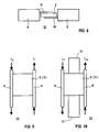
- FIGS. 2 to 5 each show a force sensor in the force-free state (part a) and under the action of a force (part b), 6 shows a diagram with respect to the magnetostriction coefficient as a function of the layer thickness of a magnetostrictive layer such as Figures 7 to 12 special embodiments of sensor devices.
- FIGS. 2 to 5 each show a force sensor in the force-free state (part a) and under the action of a force (part b)
- 6 shows a diagram with respect to the magnetostriction coefficient as a function of the layer thickness of a magnetostrictive layer such as Figures 7 to 12 special embodiments of sensor devices.
- Corresponding parts are provided with the same reference numerals in the figures.
- FIG. 1 shows an oblique view of an embodiment of a force sensor 2 for a sensor device according to the invention in thin-film technology.
- the force sensor 2 comprises a multilayer system 3, which in its basic form contains a magnetic base layer 4, a non-magnetic intermediate layer 5 and a further magnetic layer 6 with a layer thickness or height h.
- a magnetization M1 is firmly embossed in the base layer 4, while a magnetization M2 in the further layer 6 can be changed by the action of a force.
- the base layer 4 is therefore comparatively magnetically harder than the further layer 6. Since the base layer generates a magnetic background (so-called “bias field”), it is often also referred to as a bias layer.
- the magnetically softer layer 6 is essentially only the layer that is sensitive to an external force effect, it can therefore be regarded as a detection or measurement layer.
- the base layer can also be formed in a manner known per se by a layer system which, for example, represents an artificial antiferromagnet (cf. WO 94/15223).
- the multilayer system 3 can preferably be giant magnetoresistive (so-called "GMR system”), tunnel magnetoresistive (so-called “TMR system”) or colossal magnetoresistive (so-called "CMR system”) and accordingly in a known manner a GMR or TMR or XMR -System with an increased magnetoresistive effect (see, for example, the volume "XMR Technologies" Technology Analysis: Magnetism; Vol.
- the intermediate layer 5 then consists of a metallic material such as Cu (for example for a GMR system) or of an insulating material such as Al 2 O 3 (for example for a TMR system).
- the measuring layer 6 is intended to be a magnetostrictive Be formed part of the force sensor 2, the in the absence of a force or measuring field, a predetermined orientation shows its magnetization M2. Layer 6 exists therefore from one of the known magnetostrictive materials.
- the layer 4 is on a Force acts in the opposite way as the layer 6th
- Is as indicated in part b of the figure is, the material of the layer 6 under the action of the force k compressed, the pressure in the material creates an anisotropy parallel to the direction of expansion of the elements 8 and 9 or perpendicular to the distance line between these elements.
- the magnetization in this Direction is turned.
- the magnetization rotated in this way is in Figure 2, part b, labeled M2 '.
- the rotation of the magnetization is made by known means, particularly in the Measurement technology using magnetostrictive and / or magnetoresistive sensors are common in a unique correlated electrical measurement signal converted (cf. e.g. the mentioned WO94 / 15223).
- the force sensors were implemented with measuring layers with positive magnetostriction. Layers with negative magnetostriction can also be used just as well. For such layers, for example, the measuring current I m has to be reversed; that is, the effect of the force is opposite, the magnetostrictive effect remaining unchanged.
- Co and / or Ni-containing magnetic layers which have a high magnetostriction coefficient ⁇ are advantageous for realizing the magnetostrictive layer.
- a characteristic of many materials is the dependence of the magnetostriction coefficient on the composition (eg measured in atomic%) and also on the layer thickness.
- the ⁇ is negative, while Co 95 Fe 5 shows almost no magnetostriction.
- Co 50 Fe 50 has a positive maximum in magnetostriction.
- the layer thickness d is decisive for the absolute size of the magnetostriction coefficient ⁇ . A corresponding dependence emerges from the diagram in FIG.
- the force sensor for the invention Sensor device also formed by a single layer his.
- This layer shows either the so-called AMR effect (cf. the mentioned volume "XMR technologies") or consists of a piezoelectric material. This alternative is for all of the embodiments shown below are applicable. Only the magnetostrictive or piezoelectric is decisive Property of the layer or layer system, where an orientation dependent on the application of force the magnetization is detected and evaluated.
- the thickness of the (conductor) elements 8 and 9 is predetermined by the technology and is in the range from a few 10 to a few 100 nm.
- the thickness of the active magnetoresistive measuring layer is in the range of a few nm.
- FIG. 7 shows a corresponding embodiment of a sensor device 20 according to the invention in top view (part a of the figure) and in cross section (part b of the figure).
- the force sensor 2 or its magnetostrictive measuring layer 6 is arranged between a first part of a current conductor forming a conductor element 8 and a second part forming a reference element 9 in a force-locking connection with these conductor parts.
- Its extent d represents the distance between the two elements 8 and 9. That is, in this embodiment, the reference element 9 is formed by a part of the same conductor, but with the opposite direction of current flow.
- the current I m through the conductor element 8 produces a magnetic field or measuring field H m which interacts with the magnetic field or reference field H r caused by the reference element 9 because of the small distance d between the two elements 8 and 9 and so creates a mutual force effect between the two elements.
- the measuring current should not interact with the magnetization in one of the layers (e.g. from XMR multilayer systems or the single layer of an AMR type).
- a force and a "classic XMR sensor dependency ie a simultaneous effectiveness of the magnetic field with two different magnetic effects (XMR and magnetostriction).
- An arrangement of the force sensor between the current-carrying conductor element and the reference element is then possible in this way that it is additionally sensitive to perpendicular magnetic fields, for example a GMR sensor of the CPP type ( C urrent P erpendicular to P lane; cf. WO 94/15223).
- the flat side of the sensor and the field-generating elements are in here same or in parallel planes, in which case at least one magnetic field-sensitive layer should be one which can be magnetized perpendicularly, but which has a preferred direction of magnetization in the plane.
- Embodiment of a sensor device 20 is required it is not necessarily extensive training. Because for materials with a magnetostrictive sensitivity in one In the other direction, you can also turn the superstructure accordingly realize.
- sensor devices according to the invention are the assumption the magnetostrictive sensitivity in a wafer plane. This results in the following basic arrangements in the cross section of Figure 7, part b: According to this figure should the magnetostrictive measuring layer 6 between two Elements 8 and 9 are the resulting field components only occur vertically. It can be used for magnetic Interactions with magnetic layers of the force sensor Avoid 2.
- the embodiment of Figure 7, part b is particularly for the TMR and the vertical GMR effect with so-called CIP contacting (cf. WO 94/15223) favorable because the signal here through a current flow from top to bottom or vice versa can be evaluated.
- the force sensor does not need any To have contact with the current-carrying elements.
- layers whose change in resistance is read out in a wafer plane must be, e.g. for GMR systems with CIP contacting (see WO 94/15223) or AMR layers, the signal can the individual conductors can be tapped.
- the conductor arrangement according to FIG. 7 is particularly advantageous for digital current transformers.
- the effect of the current with it itself leads to a quadratic interaction.
- At different current levels for the two logic states e.g. 4 mA: LOW; 20 mbar: HIGH
- the flowing current can be without significant retroactive effects can be used again.
- the signal can also can be tapped via the conductor elements 8 and 9 itself.
- the layer system of the force sensor is on each side 2 contacted from above or below.
- a corresponding embodiment a sensor device 21 with contacting parts 18 and 19 of its elements 8 and 9 goes from the cross section of the Figure 8 out.
- the embodiment of a sensor device 21 shown in a top view in FIG. 9 differs from the sensor device 22 according to FIG. 7 only in that its reference element 9 'is formed by a current conductor which is separate from the circuit of the conductor element 8 and carries a reference current I r .
- the reference current I r which is independent of the measuring current I m, is advantageous. This achieves a linear behavior of the sensor, the characteristic of which can be set like a measuring range. Both positive and negative currents can be applied. Inverting behavior can be achieved in this simple manner. If no (reference or measurement) current is applied, the sensor device is switched to passive, ie inactive.
- the sensor device can thus also be used as a preliminary stage to a logic element, for example as an AND gate.
- the possibility of passive switching of the interaction allows the measuring current I m to be scanned with a scanning pulse on the reference (conductor) element 9 '.
- the amplitude and the number of integrated measuring pulses determine the sensitivity and accuracy.
- a suitable pulse / pause ratio can also reduce power consumption, among other things.
- a sinusoidal current is favorable as a reference variable because the magnetostriction can then be read out very sensitively, for example with a lock-in amplifier.
- the measuring current can then be further processed if necessary.
- the reference element 9 ′ can be used to select a second measurement current I m 2 , which can be selected independently of the measurement current I m1 through the (first) conductor element 8.
- the characteristic curve of the force interaction then allows the use of the sensor device as a mixer for electrical currents. For example, frequency transformations can be carried out. Both measuring currents I m1 and I m2 can be processed further.
- the figure also shows possible connection conductors 10 and 11 for the force sensor 2 of the device 23.
- the force sensor can also be formed here by a magnetoresistive multilayer system, by a single magnetoresistive layer or by a piezoelectric layer.
- the sensor device according to the invention can also have a plurality of force sensors which are to be placed under pressure or tension by a measuring current I m .
- FIG. 11 shows a top view of a corresponding embodiment of a sensor device 24, which has two force sensors 2 and 2 ′ symmetrical to a conductor element 8 through which a measuring current I m flows.
- a reference element 9 'carrying a reference current I r1 or I r2 is arranged non-positively on the outside thereof opposite the conductor element 8.
- the magnetic field of a conductor and thus the effect can be amplified by a coil arrangement, for example by looping the reference current conductor 9 '.
- the sensor device 24 shown in FIG. 11 offers itself, in which a kind of bridge with a conductor in the Middle and same current directions I r1 and I r2 in the reference (conductor) elements 9 'are realized on the outside. This is because the measurement signal is doubled.
- FIG. 12 shows, in a representation corresponding to FIG. 7, a corresponding sensor device 25 in top view (part a of the figure) or in cross section (part b of the figure).
- the magnetic field lines 30 of a corresponding permanent magnetic reference element 29 are illustrated in the figure.
- the reference element 29 is advantageously structured such that the field lines 30 are as perpendicular as possible to the measurement current I m .
- a high force with low energy consumption can be achieved by using the permanent magnetic reference element instead of a second conductor.
- the measuring current I m can be processed further by the conductor element 8.
- an embodiment corresponding to FIG. 11 is possible with two reference elements, between which the conductor element 8 through which the measuring current I m lies lies.
Landscapes
- Physics & Mathematics (AREA)
- General Physics & Mathematics (AREA)
- Measuring Instrument Details And Bridges, And Automatic Balancing Devices (AREA)
- Measurement Of Current Or Voltage (AREA)
- Hall/Mr Elements (AREA)
- Measuring Fluid Pressure (AREA)
Abstract
Description
Die Erfindung betrifft ferner die Verwendung einer solchen Sensoreinrichtung.
- auf ihn eine von dem Stromfluss abhängende Kraft (mechanisch) einwirkt,
- er einen -magnetostriktiven Teil mit einer bei fehlendem Messfeld vorbestimmten Ausrichtung der Magnetisierung umfasst, die unter der Kraftwirkung ihre Richtung ändert,
- und er Mittel zur Umwandlung der Richtungsänderung der Magnetisierung in ein eindeutig damit korreliertes elektrisches Messsignal enthält.
deren Figur 1 den prinzipiellen Aufbau eines Kraftsensors für eine Sensoreinrichtung,
deren Figuren 2 bis 5 jeweils einen Kraftsensor im kraftfreien Zustand (Teil a) und unter Einwirkung einer Kraft (Teil b),
deren Figur 6 ein Diagramm bezüglich des Magnetostriktions-Koeffizienten in Abhängigkeit von der Schichtdicke einer magnetostriktiven Schicht
sowie
deren Figuren 7 bis 12 spezielle Ausführungsformen von Sensoreinrichtungen.
Dabei sind in den Figuren sich entsprechende Teile mit denselben Bezugszeichen versehen.
Gemäß einem konkreten Beispiel für die Kraftwirkung gemäß vorstehender Formel sei angenommen:
Claims (13)
- Sensoreinrichtung (20 bis 24) zur indirekten Strommessungsowiea) mit wenigstens einem elektrischen Leiterelement (8), das mittels Stromfluss ein magnetisches Messfeld (Hm) erzeugt,b) mit mindestens einem Referenzelement (9, 9'), das von dem Leiterelement (8) beabstandet ist und ein magnetisches Referenzfeld (Hr) erzeugt, welches mit dem Messfeld (Hm) wechselwirkt,c) mit wenigstens einem zwischen dem Referenzelement und dem Leiterelement angeordneten Kraftsensor (2, 2'),undc1) auf den eine von dem Stromfluss abhängende Kraft (k, k') einwirkt,c2) der einen magnetostriktiven Teil mit einer bei fehlendem Messfeld (Hm) vorbestimmten Ausrichtung der Magnetisierung (M2) umfasst, die unter der Kraftwirkung ihre Richtung ändert,c3) der Mittel zur Umwandlung der Richtungsänderung der Magnetisierung (M2') in ein eindeutig damit korreliertes elektrisches Messsignal enthält.
- Sensoreinrichtung nach Anspruch 1, dadurch gekennzeichnet, dass die Umwandlungsmittel wenigstens ein dem magnetostriktiven Teil zugeordnetes magnetoresistives Element sind.
- Einrichtung nach Anspruch 2, dadurch gekennzeichnet, dass die Umwandlungsmittel ein magnetoresistives Mehrschichtensystem (3) sind mit wenigstens einer den magnetostriktiven Teil bildenden Schicht (6).
- Einrichtung nach Anspruch 2 oder 3, dadurch gekennzeichnet, dass das magnetoresistive Element vom AMR- oder vom GMR- oder vom TMR- oder vom XMR-Typ ist.
- Einrichtung nach einem der vorangehenden Ansprüche, dadurch gekennzeichnet, dass der magnetostriktive Teil des Kraftsensors durch eine magnetoresistive oder piezoelektrische Schicht gebildet ist.
- Einrichtung nach einem der vorangehenden Ansprüche, dadurch gekennzeichnet, dass das Referenzelement (9) und das Leiterelement (8) Teile eines gemeinsamen Leiters sind und entgegengesetzte Stromflussrichtungen aufweisen.
- Einrichtung nach einem der Ansprüche 1 bis 5, dadurch gekennzeichnet, dass das Referenzelement (9) von einem Stromleiter mit entgegengesetzter Stromrichtung gebildet ist, der getrennt vom Stromkreis des Leiterelementes (8) ist.
- Einrichtung nach einem der Ansprüche 1 bis 5 dadurch gekennzeichnet, dass das Referenzelement von einem permanentmagnetischen Element (29) gebildet ist.
- Einrichtung nach einem der vorangehenden Ansprüche, dadurch gekennzeichnet, dass der Kraftsensor zusätzlich in einem magnetischen Hintergrundfeld angeordnet ist.
- Einrichtung nach einem der vorangehenden Ansprüche, gekennzeichnet durch eine Ausbildung in Dünnschichttechnik.
- Verwendung der Sensoreinrichtung nach einem der vorangehenden Ansprüche als ein Element der Messtechnik oder der Datenverarbeitung.
- Verwendung der Sensoreinrichtung nach Anspruch 11 als digitaler Stromwandler.
- Verwendung der Sensoreinrichtung nach Anspruch 11 als Vorstufe zu einem digitalen Logikelement.
Applications Claiming Priority (4)
| Application Number | Priority Date | Filing Date | Title |
|---|---|---|---|
| DE10137700 | 2001-08-01 | ||
| DE10137700 | 2001-08-01 | ||
| DE10227561 | 2002-06-20 | ||
| DE10227561A DE10227561A1 (de) | 2001-08-01 | 2002-06-20 | Sensoreinrichtung zur indirekten Strommessung |
Publications (4)
| Publication Number | Publication Date |
|---|---|
| EP1281975A2 true EP1281975A2 (de) | 2003-02-05 |
| EP1281975A3 EP1281975A3 (de) | 2003-07-16 |
| EP1281975B1 EP1281975B1 (de) | 2008-03-05 |
| EP1281975B8 EP1281975B8 (de) | 2008-04-23 |
Family
ID=26009848
Family Applications (1)
| Application Number | Title | Priority Date | Filing Date |
|---|---|---|---|
| EP20020016112 Expired - Lifetime EP1281975B8 (de) | 2001-08-01 | 2002-07-19 | Sensoreinrichtung zur indirekten Strommessung |
Country Status (2)
| Country | Link |
|---|---|
| EP (1) | EP1281975B8 (de) |
| DE (1) | DE50211812D1 (de) |
Cited By (1)
| Publication number | Priority date | Publication date | Assignee | Title |
|---|---|---|---|---|
| CN116184001A (zh) * | 2023-04-24 | 2023-05-30 | 南方电网数字电网研究院有限公司 | 一种基于磁电效应的电流传感器 |
Family Cites Families (4)
| Publication number | Priority date | Publication date | Assignee | Title |
|---|---|---|---|---|
| US4528502A (en) * | 1982-10-01 | 1985-07-09 | General Electric Company | Current sensor |
| DE4243358A1 (de) * | 1992-12-21 | 1994-06-23 | Siemens Ag | Magnetowiderstands-Sensor mit künstlichem Antiferromagneten und Verfahren zu seiner Herstellung |
| JPH06288844A (ja) * | 1993-03-31 | 1994-10-18 | Matsushita Electric Ind Co Ltd | 力学量センサ |
| DE19753554A1 (de) * | 1997-12-03 | 1999-07-08 | Bosch Gmbh Robert | Aktiver Magnetfeld-Kraftsensor |
-
2002
- 2002-07-19 DE DE50211812T patent/DE50211812D1/de not_active Expired - Lifetime
- 2002-07-19 EP EP20020016112 patent/EP1281975B8/de not_active Expired - Lifetime
Cited By (2)
| Publication number | Priority date | Publication date | Assignee | Title |
|---|---|---|---|---|
| CN116184001A (zh) * | 2023-04-24 | 2023-05-30 | 南方电网数字电网研究院有限公司 | 一种基于磁电效应的电流传感器 |
| CN116184001B (zh) * | 2023-04-24 | 2023-09-15 | 南方电网数字电网研究院有限公司 | 一种基于磁电效应的电流传感器 |
Also Published As
| Publication number | Publication date |
|---|---|
| EP1281975B1 (de) | 2008-03-05 |
| EP1281975B8 (de) | 2008-04-23 |
| EP1281975A3 (de) | 2003-07-16 |
| DE50211812D1 (de) | 2008-04-17 |
Similar Documents
| Publication | Publication Date | Title |
|---|---|---|
| DE102006035661B4 (de) | Magnetfelderfassungsvorrichtung und Verfahren zu deren Einstellung | |
| EP0674769B1 (de) | Magnetowiderstands-sensor mit künstlichem antiferromagneten und verfahren zu seiner herstellung | |
| DE102007032867B4 (de) | Magnetoresistive Magnetfeldsensorstrukturen und Herstellungsverfahren | |
| DE10017374B4 (de) | Magnetische Koppeleinrichtung und deren Verwendung | |
| EP0674770B1 (de) | Magnetowiderstands-sensor mit verkürzten messschichten | |
| DE102020103432B4 (de) | Magnetsensor | |
| DE10319319A1 (de) | Sensoreinrichtung mit magnetostriktivem Kraftsensor | |
| DE112010000890T5 (de) | Magnetfeld-Erfassungsvorrichtung | |
| DE10214946B4 (de) | TMR-Sensor | |
| DE102016102601B4 (de) | Magnetsensor | |
| DE102009007479A1 (de) | Dünnfilm-Magnetsensor | |
| DE102004032482B4 (de) | Sensor und Verfahren zum Erfassen einer Verformung | |
| DE112016000720B4 (de) | Sensoranordnung zur Positionserfassung und Verfahren zum Unterstützen des Bestimmens der Position eines Objekts | |
| WO2012126693A1 (de) | Vorrichtung und verfahren zum messen von magnetfeldern | |
| DE69407194T2 (de) | Magnetoresistiver stromsensor und verfahren zu seiner herstellung | |
| DE60307523T2 (de) | Verfahren zum messen der magnetostriktion in magnetowiderstandselementen | |
| DE102007032299B4 (de) | Sensor, insbesondere zur Magnetfeldmessung | |
| DE69432967T2 (de) | Magnetfeldsonde in Dünnschichtechnik | |
| DE102005009390B3 (de) | Kraftsensor, Verfahren zur Ermittlung einer auf einen Kraftsensor wirkenden Kraft mittels eines Mehrschichtsystems aus magnetischen Schichten | |
| EP2333567B1 (de) | Vorrichtung zur Strommessung | |
| EP0730162A2 (de) | Sensoreinrichtung mit einer Brückenschaltung von magnetoresistiven Sensorelementen | |
| DE102010038287B4 (de) | Magnetfeld-Sensorvorrichtung, entsprechendes Herstellungsverfahren und Magnetfeld-Messverfahren | |
| EP1281975B1 (de) | Sensoreinrichtung zur indirekten Strommessung | |
| DE10227561A1 (de) | Sensoreinrichtung zur indirekten Strommessung | |
| DE102021201042B3 (de) | Magnetfeldsensorvorrichtung und Verfahren zum Herstellen einer Magnetfeldsensorvorrichtung |
Legal Events
| Date | Code | Title | Description |
|---|---|---|---|
| PUAI | Public reference made under article 153(3) epc to a published international application that has entered the european phase |
Free format text: ORIGINAL CODE: 0009012 |
|
| AK | Designated contracting states |
Designated state(s): AT BE BG CH CY CZ DE DK EE ES FI FR GB GR IE IT LI LU MC NL PT SE SK TR |
|
| AX | Request for extension of the european patent |
Extension state: AL LT LV MK RO SI |
|
| PUAL | Search report despatched |
Free format text: ORIGINAL CODE: 0009013 |
|
| AK | Designated contracting states |
Designated state(s): AT BE BG CH CY CZ DE DK EE ES FI FR GB GR IE IT LI LU MC NL PT SE SK TR |
|
| AX | Request for extension of the european patent |
Extension state: AL LT LV MK RO SI |
|
| 17P | Request for examination filed |
Effective date: 20030804 |
|
| AKX | Designation fees paid |
Designated state(s): DE FR IT |
|
| 17Q | First examination report despatched |
Effective date: 20041006 |
|
| GRAP | Despatch of communication of intention to grant a patent |
Free format text: ORIGINAL CODE: EPIDOSNIGR1 |
|
| GRAS | Grant fee paid |
Free format text: ORIGINAL CODE: EPIDOSNIGR3 |
|
| GRAA | (expected) grant |
Free format text: ORIGINAL CODE: 0009210 |
|
| AK | Designated contracting states |
Kind code of ref document: B1 Designated state(s): DE FR IT |
|
| RAP2 | Party data changed (patent owner data changed or rights of a patent transferred) |
Owner name: VDO AUTOMOTIVE AG |
|
| REF | Corresponds to: |
Ref document number: 50211812 Country of ref document: DE Date of ref document: 20080417 Kind code of ref document: P |
|
| RAP2 | Party data changed (patent owner data changed or rights of a patent transferred) |
Owner name: CONTINENTAL AUTOMOTIVE GMBH |
|
| ET | Fr: translation filed | ||
| PLBE | No opposition filed within time limit |
Free format text: ORIGINAL CODE: 0009261 |
|
| STAA | Information on the status of an ep patent application or granted ep patent |
Free format text: STATUS: NO OPPOSITION FILED WITHIN TIME LIMIT |
|
| 26N | No opposition filed |
Effective date: 20081208 |
|
| REG | Reference to a national code |
Ref country code: FR Ref legal event code: TP Owner name: CONTINENTAL AUTOMOTIVE GMBH, DE Effective date: 20111104 |
|
| REG | Reference to a national code |
Ref country code: FR Ref legal event code: PLFP Year of fee payment: 15 |
|
| REG | Reference to a national code |
Ref country code: FR Ref legal event code: PLFP Year of fee payment: 16 |
|
| REG | Reference to a national code |
Ref country code: FR Ref legal event code: PLFP Year of fee payment: 17 |
|
| PGFP | Annual fee paid to national office [announced via postgrant information from national office to epo] |
Ref country code: DE Payment date: 20180731 Year of fee payment: 17 Ref country code: FR Payment date: 20180725 Year of fee payment: 17 Ref country code: IT Payment date: 20180724 Year of fee payment: 17 |
|
| REG | Reference to a national code |
Ref country code: DE Ref legal event code: R119 Ref document number: 50211812 Country of ref document: DE |
|
| PG25 | Lapsed in a contracting state [announced via postgrant information from national office to epo] |
Ref country code: DE Free format text: LAPSE BECAUSE OF NON-PAYMENT OF DUE FEES Effective date: 20200201 |
|
| REG | Reference to a national code |
Ref country code: DE Ref legal event code: R081 Ref document number: 50211812 Country of ref document: DE Owner name: VITESCO TECHNOLOGIES GMBH, DE Free format text: FORMER OWNER: CONTINENTAL AUTOMOTIVE GMBH, 30165 HANNOVER, DE |
|
| PG25 | Lapsed in a contracting state [announced via postgrant information from national office to epo] |
Ref country code: FR Free format text: LAPSE BECAUSE OF NON-PAYMENT OF DUE FEES Effective date: 20190731 |
|
| PG25 | Lapsed in a contracting state [announced via postgrant information from national office to epo] |
Ref country code: IT Free format text: LAPSE BECAUSE OF NON-PAYMENT OF DUE FEES Effective date: 20190719 |