EP1281663A2 - Method of manufacture of micromechanical structures - Google Patents
Method of manufacture of micromechanical structures Download PDFInfo
- Publication number
- EP1281663A2 EP1281663A2 EP02012141A EP02012141A EP1281663A2 EP 1281663 A2 EP1281663 A2 EP 1281663A2 EP 02012141 A EP02012141 A EP 02012141A EP 02012141 A EP02012141 A EP 02012141A EP 1281663 A2 EP1281663 A2 EP 1281663A2
- Authority
- EP
- European Patent Office
- Prior art keywords
- layer
- silicon wafer
- structures
- masking layer
- produced
- Prior art date
- Legal status (The legal status is an assumption and is not a legal conclusion. Google has not performed a legal analysis and makes no representation as to the accuracy of the status listed.)
- Withdrawn
Links
Images


Classifications
-
- B—PERFORMING OPERATIONS; TRANSPORTING
- B81—MICROSTRUCTURAL TECHNOLOGY
- B81C—PROCESSES OR APPARATUS SPECIALLY ADAPTED FOR THE MANUFACTURE OR TREATMENT OF MICROSTRUCTURAL DEVICES OR SYSTEMS
- B81C1/00—Manufacture or treatment of devices or systems in or on a substrate
- B81C1/00388—Etch mask forming
- B81C1/00428—Etch mask forming processes not provided for in groups B81C1/00396 - B81C1/0042
-
- B—PERFORMING OPERATIONS; TRANSPORTING
- B81—MICROSTRUCTURAL TECHNOLOGY
- B81C—PROCESSES OR APPARATUS SPECIALLY ADAPTED FOR THE MANUFACTURE OR TREATMENT OF MICROSTRUCTURAL DEVICES OR SYSTEMS
- B81C1/00—Manufacture or treatment of devices or systems in or on a substrate
- B81C1/00777—Preserve existing structures from alteration, e.g. temporary protection during manufacturing
- B81C1/00785—Avoid chemical alteration, e.g. contamination, oxidation or unwanted etching
- B81C1/00801—Avoid alteration of functional structures by etching, e.g. using a passivation layer or an etch stop layer
-
- B—PERFORMING OPERATIONS; TRANSPORTING
- B81—MICROSTRUCTURAL TECHNOLOGY
- B81C—PROCESSES OR APPARATUS SPECIALLY ADAPTED FOR THE MANUFACTURE OR TREATMENT OF MICROSTRUCTURAL DEVICES OR SYSTEMS
- B81C1/00—Manufacture or treatment of devices or systems in or on a substrate
- B81C1/00865—Multistep processes for the separation of wafers into individual elements
- B81C1/00896—Temporary protection during separation into individual elements
Definitions
- the invention relates to a method for generating micromechanical Structures in a silicon wafer or in the functional layer of a layer structure for surface micromechanics, the silicon wafer or the functional layer is provided with at least one first masking layer, which is structured in this way will that part of the micromechanical structures to be generated in an etching process, and wherein the silicon wafer masked in this way or the functional layer masked in this way at least one first etching process is subjected, after which the corresponding first masking layer is removed.
- a first masking layer is first applied to the wafer surface, which is intended for the flat trench etching process.
- a second masking layer is applied to the first masking layer applied, which is intended for deep trench etching.
- the second Masking layer is made exclusively according to the geometry of the rough structure structured.
- the present invention proposes a method with which different Structures such as Coarse structures and fine structures, independently from each other in a silicon wafer or also in the functional layer Layer structure for surface micromechanics can be generated.
- the silicon wafer or the Functional layer after the at least one first etching process and the removal of the at least one first masking layer at least once with one another masking layer is provided, so that the structures already generated are protected against a further etching attack.
- This further masking layer will structured before the silicon wafer or the functional layer masked in this way undergoes a further etching process and the further masking layer is removed after the further etching process.
- the different micromechanical structures generated in succession in different etching processes are created by an appropriate masking layer before a further etching attack protected if the structure is no longer to be specifically changed.
- the individual etching processes are completely independent of one another.
- the number of etching processes of the method according to the invention is therefore not restricted through uncontrolled effects on structures already created, so that overall micromechanical structures can be generated, the Complexity far beyond the complexity of the realizable with the known method Structures.
- a photoresist layer with positive or negative exposure properties has proven to be a masking layer in particular when etching small structures as advantageous.
- a layer of photoresist can be made using standard methods are applied to the silicon wafer or the functional layer and can be structured using the easy-to-use methods of photo technology.
- a Resist mask has both a structuring and an etching process covering function.
- CVD layers can be used as masking layers with the help a resist layer can also be easily structured.
- a already pre-structured silicon wafers or an already pre-structured functional layer a permanent resist in the form of a lacquer film on the respective surface laminated on, the structures already created being covered but not lined become.
- a lacquer film both fine structures and Cover coarse structures easily and reliably because of this type of masking is independent of the structure to be protected that has already been created.
- Covering of the structures already created with a fixed resist compared to lining These structures, for example with a liquid resist, have the advantage that the Masking layer can not tear off at the topography, so that the particularly sensitive edge areas of the structures already created to be protected. This is called good edge coverage. Since that Removal is not permanent penetration into the structures already created of such a masking layer also of fine structures is unproblematic
- the masking layer is related to the structure already created. That is why the masking layer in another variant of the method according to the invention in the form a liquid resist or in the form of a CVD layer on the silicon wafer or the functional layer applied so that the liquid resist varnish already in the generated structures penetrates and at least lines them or even completely fills.
- liquid resist varnish with the help of a dispenser Apply silicon wafer or the functional layer or in the already generated Bring structures.
- This variant is particularly suitable for filling out of micromechanical fine structures with liquid resist lacquer, since the lacquer quantities and the spray positions of the dispenser can be precisely defined. This allows one or more spraying processes per structure exactly the amount of protective lacquer that is to be placed over the structures level filling of the structures is required.
- the structures can be used in the process according to the invention can be produced using both isotropic and anisotropic etching processes.
- Anisotropic etching processes such as e.g. the Trenchen, also known as Plasma RIE, in which the etching attack is essentially only perpendicular to the attack surface, i.e. in the Depth, is directed. Therefore, the silicon wafer or the functional layer in an advantageous variant of the method according to the invention at least one Trenched.
- Masking layers in the form of a photoresist layer - solid resist or liquid resist - can be dry chemically, for example in an O2 plasma stripper, as well as wet chemical removal using a suitable solvent. There When the resist layer is removed dry, particles remain on the wafer surface can, both in a subsequent masking as well can interfere with a subsequent etching process is recommended the use of a wet chemical process. Has proven to be particularly reliable a combination of dry chemical removal with subsequent wet chemical removal.
- the invention offers Process the possibility of the fine structure of the silicon wafer or the functional layer in front of the rough structure.
- fine structures can now also be used in the area of a rough structure that has already been created. Since the invention Procedure on both the front and the back a silicon wafer or a layer structure can be used, can by combining structures from the two main surfaces have been created, structures are created that span the entire Extend thickness of the silicon wafer or the layer structure. To this In this way it is also very easy to connect connecting bridges between pre-processed ones Generate chips to separate these chips.
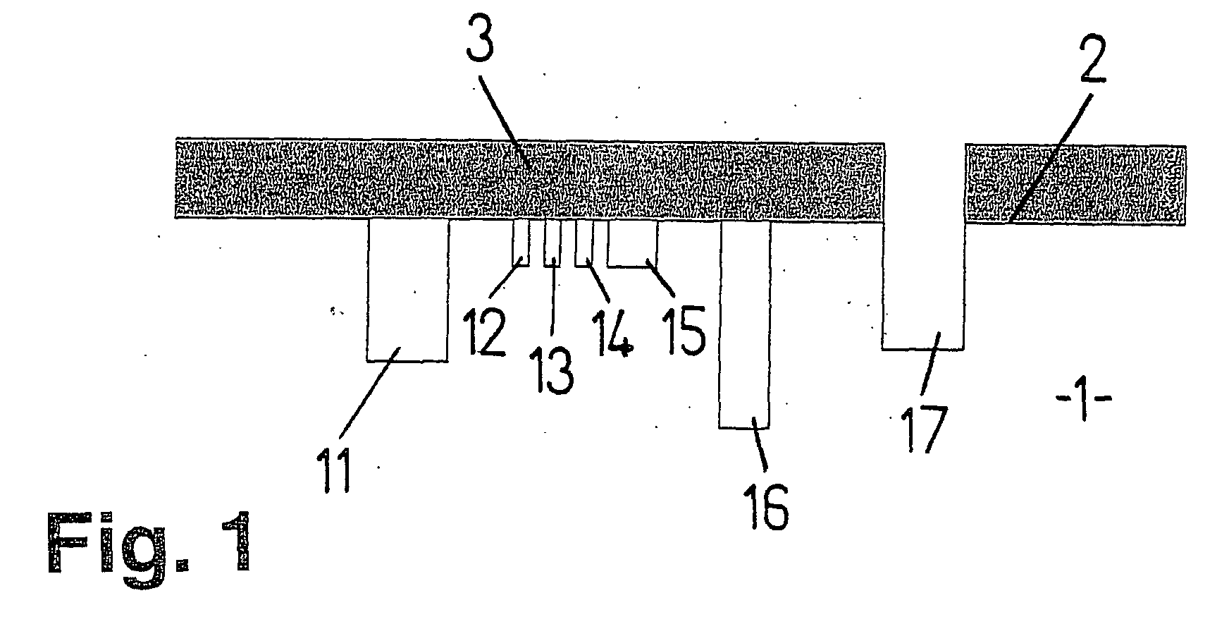
- etching recesses 11 up to 17 different widths and depths These etch recesses 11 to 17 are in four successive with the help of the inventive method and independent trench processes have been generated and accordingly have 2 side walls oriented perpendicular to the surface on.
- a masking layer was applied to the Surface 2 of the silicon wafer 1 applied.
- the first masking layer was like this structured that only the fine structure in the form of the Etching recesses 12 to 15 was generated. After that, the first masking layer away.
- the etching recess 11 was produced in a further etching process, which is much wider and deeper than the etching recesses 12 to 15 of the Fine structure.
- the surface 2 of the silicon wafer 1 was masked again, so that the fine structure was protected against the subsequent etching attack.
- This the second masking layer has now been structured to separate the etching recess 11, So that only in the area of the etching recess to be produced 11 an etching attack could take place.
- the second masking layer is removed again.
- the same procedure became Generating the etching recess 16 repeatedly, with the third masking layer now not only the fine structure but also the etching recess 11 are covered and was protected against another caustic attack.
- the etching recess 16 is narrower but deeper than the etching recess 11, so that the third trenching process probably took longer than the second trench process.
- the third masking layer was also removed.
- 1 is the silicon wafer 1 after the fourth trenching process, in which only the etching recess 17 is produced has been shown, but before removing the fourth masking layer 3.
- the method according to the invention offers the possibility of the sequence to vary the individual etching processes as desired. That it can now be finer Structures before coarser structures as well as coarser structures before finer ones Structures can be created in a silicon wafer. On the other hand, you can any number of etching processes can be carried out in succession without doing so once structures have been created are changed in an uncontrolled manner. That way you can etch recesses of different depths in a silicon wafer without any problems and thus also relatively complex structures are created.
- the method according to the invention also offers the possibility of being independent of one another Structures in the front and back of a silicon wafer to etch and combine these structures with one another, which is illustrated by FIG. 2 becomes.
- a silicon wafer 20 is shown in the front Etching recesses 21 to 24 and in the back of etching recesses a to d have been trenched.
- a combination of front and back structures The back is exemplary of the combinations of the etching recesses 23 and c as well as 24 and d to see.
- a membrane is denoted by e here depending on the type of double-sided etching attack at any depth of a silicon wafer can be generated. The thickness of the membrane e is determined by the combination the depths of the etching recesses 22 and b defined.
- the method according to the invention can also be used for structuring a silicon wafer used with pre-processed chips to separate the chips, which is illustrated by Figures 3 and 4.
- Fig. 3 Variant, the front of the silicon wafer was masked so that the preprocessed Chips 31 and 32 were protected against an etching attack. Then was the silicon in the spaces between the chips in a trenching process etched out to a certain depth, leaving chips 31 and 32 only are connected to one another via thin silicon webs 33.
- the Trenching can also be stopped on another material, e.g. on an oxide or on a bonded silicon wafer or glass wafer. To the Separately, the chips 31 and 32 can then simply be broken apart become.
- By combining one from the front and one Etching attack starting from the back of the silicon wafer can also be connecting webs 45 between the individual chips 41 to 44 are generated, such as they are shown in Fig. 4.
- a solid resist was in the form of a lacquer film 55 with positive or negative exposure properties as a second masking layer used.
- Such paint films can be easily, regardless of the Laminate structures already created in the wafer surface onto the silicon wafer and then cover the structures already created, here the etching recess 51, without penetrating into it. In this way, the Edges of an already created structure are good against a further etching attack protect.
- a solid resist can be just like a liquid resist layer using standard methods of photographic technology, such as exposure and development, edited or structured become.
- the lacquer film 55 was in the area of the generating etching recess 54 removed to an etching attack on the bottom surface 52 to enable the etching recess 51.
- the subsequent trenching process in spite of partial masking of the etching recess 51, it can be too overetching of the etching recess 51, since the side walls 54 the etching recess 51 are unprotected.
- the second masking layer with the one already created Structure is related, as in the variant shown in Fig. 5b.
- the resist must be introduced as evenly as possible into the structure that has already been produced so that the entire wall of the structure is protected.
- To the A liquid resist lacquer was therefore used to line the etching recess 51.
- the lacquer layer 56 was structured with the aid of a projection exposure. The lacquer layer 56 was only on the bottom surface 52 of the etching recess 51 removed in the area of the etching recess 54 to be produced, so that also the side wall 53 of the etching recess 51 against an etching attack during the subsequent trenching process was protected.
- a liquid resist lacquer can be used also with the help of a dispenser through single or multiple spraying operations applied the silicon wafer and in particular in depressions in the wafer surfaces be introduced.
- the spray positions can be pre-programmed or automatically recognized and started using an image processing system become.
- the micromechanical already generated Structures can also be coated with the protective lacquer. Because the amount of paint and the spraying positions can be precisely defined by means of an or Repeated spraying processes per structure exactly the amount of protective lacquer placed above the structures required to fill the structures evenly is.
- the stripping of the newly etched structures is both when using a fixed resist and when using of a liquid resist is not critical.
- Fixed resist films may not be possible Remove completely dry, as parts of the lamination layer as silicon residues or residues containing silicon oxide remain on the wafer and later act as a particle source.
- a permanent resist film is therefore advantageous removed by wet chemical means. It is also possible to dry-dry most of the resist, for example in an oxygen plasma stripper to remove the Then remove laminate residues wet-chemical and, if necessary, the remaining ones organic residues completely in another dry chemical process to remove.
- Liquid resist can also advantageously be combined in one Remove dry chemical and wet chemical process.
Landscapes
- Engineering & Computer Science (AREA)
- Manufacturing & Machinery (AREA)
- Microelectronics & Electronic Packaging (AREA)
- Micromachines (AREA)
- Weting (AREA)
- Drying Of Semiconductors (AREA)
Abstract
Mit der vorliegenden Erfindung wird ein Verfahren vorgeschlagen, mit dem unterschiedliche Strukturen, wie z.B. Grobstrukturen und Feinstrukturen, unabhängig voneinander in einem Siliziumwafer oder in der Funktionsschicht eines Schichtaufbaus für Oberflächenmikromechanik erzeugt werden können.The present invention proposes a method with which different Structures such as Coarse structures and fine structures, independently one another in a silicon wafer or in the functional layer of a layer structure can be generated for surface micromechanics.
Dazu wird der Siliziumwafer (1) bzw. die Funktionsschicht zunächst mit mindestens
einer ersten Maskierschicht versehen, die so strukturiert wird, dass ein
Teil der zu erzeugenden Strukturen (11 bis 17) in einem Ätzvorgang erzeugt werden
kann. Der so maskierte Siliziumwafer (1) bzw. die so maskierte Funktionsschicht
wird dann mindestens einem ersten Ätzvorgang unterzogen, nach dem die
entsprechende erste Maskierschicht entfernt wird. Erfindungsgemäß wird der Siliziumwafer
(1) bzw. die Funktionsschicht nach dem mindestens einen ersten Ätzvorgang
und dem Entfernen der mindestens einen ersten Maskierschicht mindestens
einmal mit einer weiteren Maskierschicht (3) versehen, so dass die bereits
erzeugten Strukturen (11 bis 16) gegen einen weiteren Ätzangriff geschützt sind.
Diese weitere Maskierschicht (3) wird strukturiert, bevor der so maskierte Siliziumwafer
(1) bzw. die so maskierte Funktionsschicht einem weiteren Ätzvorgang
unterzogen wird und die weitere Maskierschicht (3) nach dem weiteren Ätzvorgang
entfernt wird.
Description
Die Erfindung betrifft ein Verfahren zum Erzeugen von mikromechanischen Strukturen in einem Siliziumwafer oder in der Funktionsschicht eines Schichtaufbaus für Oberflächenmikromechanik, wobei der Siliziumwafer bzw. die Funktionsschicht mit mindestens einer ersten Maskierschicht versehen wird, die so strukturiert wird, dass ein Teil der zu erzeugenden mikromechanischen Strukturen in einem Ätzvorgang erzeugt werden kann, und wobei der so maskierte Siliziumwafer bzw. die so maskierte Funktionsschicht mindestens einem ersten Ätzvorgang unterzogen wird, nach dem die entsprechende erste Maskierschicht entfernt wird.The invention relates to a method for generating micromechanical Structures in a silicon wafer or in the functional layer of a layer structure for surface micromechanics, the silicon wafer or the functional layer is provided with at least one first masking layer, which is structured in this way will that part of the micromechanical structures to be generated in an etching process, and wherein the silicon wafer masked in this way or the functional layer masked in this way at least one first etching process is subjected, after which the corresponding first masking layer is removed.
Es ist aus der Praxis bekannt, verschiedene Strukturen, wie z.B. Feinstrukturen und Grobstrukturen, in aufeinanderfolgenden Ätzvorgängen in einem Siliziumwafer oder der Funktionsschicht eines Schichtaufbaus für Oberflächenmikromechanik zu erzeugen. Als Funktionsschicht kann beispielsweise eine Polysiliziumschicht dienen. Für jeden dieser Ätzvorgänge ist in der Regel eine eigene Maskierschicht vorgesehen. Diese Maskierschichten werden vor dem ersten Ätzvorgang nacheinander - also übereinander - auf die Waferoberfläche bzw. die Oberfläche der Funktionsschicht aufgebracht und entsprechend der jeweils zu erzeugenden Struktur strukturiert.It is known in practice to use various structures, e.g. fine structures and coarse structures, in successive etching processes in a silicon wafer or the functional layer of a layer structure for surface micromechanics produce. For example, a polysilicon layer can serve as the functional layer. There is usually a separate masking layer for each of these etching processes intended. These masking layers are made one after the other before the first etching process - ie one above the other - on the wafer surface or the surface of the Functional layer applied and according to the one to be generated Structure structured.
Das bekannte Verfahren wird nachfolgend am Beispiel eines Siliziumwafers erläutert, in dem mit Hilfe eines Tieftrench-Ätzvorgangs eine Grobstruktur und mit Hilfe eines Flachtrench-Ätzvorgangs eine Feinstruktur erzeugt werden sollen. Dazu wird zunächst eine erste Maskierschicht auf die Waferoberfläche aufgebracht, die für den Flachtrench-Ätzvorgang bestimmt ist. Nach Strukturierung der ersten Maskierschicht wird auf die erste Maskierschicht eine zweite Maskierschicht aufgebracht, die für den Tieftrench-Ätzvorgang bestimmt ist. Die zweite Maskierschicht wird ausschließlich entsprechend der Geometrie der Grobstruktur strukturiert. Im Gegensatz dazu müssen bei der Strukturierung der ersten Maskierschicht sowohl die Geometrie der Feinstruktur als auch die Geometrie der Grobstruktur berücksichtigt werden, da der erste Ätzangriff, der Tieftrench zum Erzeugen der Grobstruktur, durch die zweite Maskierschicht und die darunter liegende erste Maskierschicht erfolgt. Nach dem Tieftrench wird die zweite Maskierschicht entfernt, so dass die Waferoberfläche beim zweiten Ätzangriff; dem Flachtrench zum Erzeugen der Feinstruktur, nur noch durch die erste Maskierschicht geschützt wird. Da die bereits erzeugte Grobstruktur nicht maskiert ist, wird die Grobstruktur auch beim Flachtrench mitgeätzt. Dabei kommt es häufig zu unerwünschten Unterätzungen der Grobstruktur, insbesondere im unteren Bereich der Ätzausnehmungen, und zu Verbreiterungen der Ätzausnehmungen.The known method is explained below using the example of a silicon wafer, in which with the help of a deep trench etching process a coarse structure and with A fine structure is to be produced with the aid of a flat trench etching process. For this purpose, a first masking layer is first applied to the wafer surface, which is intended for the flat trench etching process. After structuring the a first masking layer, a second masking layer is applied to the first masking layer applied, which is intended for deep trench etching. The second Masking layer is made exclusively according to the geometry of the rough structure structured. In contrast, when structuring the first masking layer both the geometry of the fine structure and the geometry of the Coarse structure are taken into account, since the first etching attack, the deep trench to the Generate the rough structure, through the second masking layer and the one below first masking layer takes place. After the deep trench, the second masking layer removed so that the wafer surface during the second etching attack; the Flat trench to create the fine structure, only through the first masking layer is protected. Since the rough structure already created is not masked, the coarse structure is also etched with the flat trench. It often happens undesirable undercuts of the rough structure, especially in the lower area of the etching recesses, and to widen the etching recesses.
Durch die Notwendigkeit des bekannten Verfahrens, alle Maskierschichten vor dem ersten Ätzvorgang auf die Waferoberfläche aufzubringen und nach jedem Ätzvorgang die jeweils oberste Maskierschicht einzeln zu entfernen, wird die Prozessführung stark eingeschränkt. Für die Maskierschichten müssen unterschiedliche Materialien verwendet werden, die ein selektives Entfernen der einzelnen Maskierschichten ermöglichen. Dadurch ist die Anzahl der nacheinander durchführbaren Ätzvorgänge begrenzt. Außerdem können beim selektiven Entfernen der einzelnen Maskierschichten Partikel zurückbleiben, die bei einem nachfolgenden Ätzvorgang als unerwünschte Maskierung Defekte verursachen.Due to the necessity of the known method, all masking layers before after the first etch and after each The process control involves etching the respective top masking layer individually highly limited. For the masking layers have to be different Materials are used that selectively remove each Enable masking layers. This means that the number can be carried out one after the other Etching processes limited. You can also selectively remove particles of the individual masking layers remain, which are present in a subsequent Etching process as unwanted masking cause defects.
Als besonders problematisch erweist sich, dass die einzelnen Ätzvorgänge des bekannten Verfahrens bzw. die dabei erzeugten Strukturen nicht unabhängig voneinander sind. So müssen vor den Feinstrukturen immer zunächst die Grobstrukturen erzeugt werden. Wie bereits erwähnt, werden die einmal erzeugten Strukturen nicht gegen einen weiteren Ätzangriff geschützt, so dass sie dabei zwangsläufig mitgeätzt werden. Während eine solche Überätzung bei Grobstrukturen zwar zu unerwünschten Strukturveränderungen führen kann aber zumindest in gewissem Maße tolerierbar ist, führt eine Überätzung bei Feinstrukturen in der Regel zu deren Zerstörung. Außerdem können mit dem bekannten Verfahren im Bereich einer geätzten Grobstruktur keine Feinstrukturen mehr erzeugt werden. It proves to be particularly problematic that the individual etching processes of the known method or the structures produced thereby are not independent of one another are. The coarse structures always have to be in front of the fine structures be generated. As already mentioned, the structures once created not protected against another caustic attack, so that it inevitably are also etched. While such an overetch is true for rough structures however, it can lead to undesirable structural changes, at least to some extent Measurements are tolerable, which leads to overetching in fine structures their destruction. In addition, with the known method in the field an etched coarse structure no longer produces fine structures.
Mit der vorliegenden Erfindung wird ein Verfahren vorgeschlagen, mit dem unterschiedliche Strukturen, wie z.B. Grobstrukturen und Feinstrukturen, unabhängig voneinander in einem Siliziumwafer oder auch in der Funktionsschicht eines Schichtaufbaus für Oberflächenmikromechanik erzeugt werden können.The present invention proposes a method with which different Structures such as Coarse structures and fine structures, independently from each other in a silicon wafer or also in the functional layer Layer structure for surface micromechanics can be generated.
Dies wird erfindungsgemäß dadurch erreicht, dass der Siliziumwafer bzw. die Funktionsschicht nach dem mindestens einen ersten Ätzvorgang und dem Entfernen der mindestens einen ersten Maskierschicht mindestens einmal mit einer weiteren Maskierschicht versehen wird, so dass die bereits erzeugten Strukturen gegen einen weiteren Ätzangriff geschützt sind. Diese weitere Maskierschicht wird strukturiert, bevor der so maskierte Siliziumwafer bzw. die so maskierte Funktionsschicht einem weiteren Ätzvorgang unterzogen wird und die weitere Maskierschicht nach dem weiteren Ätzvorgang entfernt wird.This is achieved according to the invention in that the silicon wafer or the Functional layer after the at least one first etching process and the removal of the at least one first masking layer at least once with one another masking layer is provided, so that the structures already generated are protected against a further etching attack. This further masking layer will structured before the silicon wafer or the functional layer masked in this way undergoes a further etching process and the further masking layer is removed after the further etching process.
Erfindungsgemäß werden die unterschiedlichen mikromechanischen Strukturen nacheinander in unterschiedlichen Ätzvorgängen erzeugt. Eine einmal erzeugte Struktur wird durch eine entsprechende Maskierschicht vor einem weiteren Ätzangriff geschützt, soweit die Struktur nicht mehr gezielt verändert werden soll. Dadurch sind die einzelnen Ätzvorgänge vollkommen unabhängig voneinander. Die Anzahl der Ätzvorgänge des erfindungsgemäßen Verfahrens wird also nicht beschränkt durch unkontrollierte Auswirkungen auf bereits erzeugte Strukturen, so dass insgesamt mikromechanische Strukturen erzeugt werden können, deren Komplexität weit über die Komplexität der mit dem bekannten Verfahren realisierbaren Strukturen hinausgeht.According to the invention, the different micromechanical structures generated in succession in different etching processes. Once created Structure is created by an appropriate masking layer before a further etching attack protected if the structure is no longer to be specifically changed. Thereby the individual etching processes are completely independent of one another. The The number of etching processes of the method according to the invention is therefore not restricted through uncontrolled effects on structures already created, so that overall micromechanical structures can be generated, the Complexity far beyond the complexity of the realizable with the known method Structures.
Grundsätzlich gibt es verschiedene Möglichkeiten für die Realisierung und für Ausgestaltungen des erfindungsgemäßen Verfahrens. Besonders vorteilhafte Varianten sind mit den nachgeordneten Patentansprüchen beansprucht und werden nachfolgend näher erläutert.Basically there are different possibilities for the realization and for Refinements of the method according to the invention. Particularly advantageous variants are and are claimed with the subordinate claims explained in more detail below.
Die Verwendung einer Photoresistschicht mit positiven oder negativen Belichtungseigenschaften als Maskierschicht erweist sich insbesondere beim Ätzen von kleinen Strukturen als vorteilhaft. Eine Photoresistschicht kann mit Standardmethoden auf den Siliziumwafer bzw. der Funktionsschicht aufgebracht werden und mit den gut handhabbaren Verfahren der Fototechnik strukturiert werden. Eine Resistmaske hat bei einem Ätzvorgang sowohl eine strukturierende als auch eine abdeckende Funktion. Im Rahmen des erfindungsgemäßen Verfahrens können aber auch CVD-Schichten als Maskierschicht verwendet werden, die mit Hilfe einer Resistschicht ebenfalls einfach strukturiert werden können.The use of a photoresist layer with positive or negative exposure properties has proven to be a masking layer in particular when etching small structures as advantageous. A layer of photoresist can be made using standard methods are applied to the silicon wafer or the functional layer and can be structured using the easy-to-use methods of photo technology. A Resist mask has both a structuring and an etching process covering function. Within the scope of the method according to the invention but also CVD layers can be used as masking layers with the help a resist layer can also be easily structured.
In einer Variante des erfindungsgemäßen Verfahrens wird zum Maskieren eines bereits vorstrukturierten Siliziumwafers bzw. einer bereits vorstrukturierten Funktionsschicht ein Festresist in Form einer Lackfolie auf die jeweilige Oberfläche auflaminiert, wobei die bereits erzeugten Strukturen abgedeckt aber nicht ausgekleidet werden. Mit einer Lackfolie lassen sich sowohl Feinstrukturen als auch Grobstrukturen einfach und zuverlässig abdecken, da diese Art der Maskierung unabhängig von der bereits erzeugten, zu schützenden Struktur ist. Das Abdecken der bereits erzeugten Strukturen mit einem Festresist hat gegenüber dem Auskleiden dieser Strukturen beispielsweise mit einem Flüssigresist den Vorteil, dass die Maskierschicht an den Topographierändern nicht abreißen kann, so dass auch die besonders empfindlichen Kantenbereiche der bereits erzeugten Strukturen gut geschützt werden. Man spricht hier von einer guten Kantenbedeckung. Da das Festresist nicht in die bereits erzeugten Strukturen eindringt, ist das Entfernen einer solchen Maskierschicht auch von Feinstrukturen unproblematischIn a variant of the method according to the invention, a already pre-structured silicon wafers or an already pre-structured functional layer a permanent resist in the form of a lacquer film on the respective surface laminated on, the structures already created being covered but not lined become. With a lacquer film, both fine structures and Cover coarse structures easily and reliably because of this type of masking is independent of the structure to be protected that has already been created. Covering of the structures already created with a fixed resist compared to lining These structures, for example with a liquid resist, have the advantage that the Masking layer can not tear off at the topography, so that the particularly sensitive edge areas of the structures already created to be protected. This is called good edge coverage. Since that Removal is not permanent penetration into the structures already created of such a masking layer also of fine structures is unproblematic
In einigen Fällen, beispielsweise wenn zunächst die Grobstrukturen im Siliziumwafer erzeugt werden und erst danach Feinstrukturen ggf. auch im Bereich der Grobstrukturen erzeugt werden sollen, ist es von Vorteil, wenn die Maskierschicht mit der bereits erzeugten Struktur zusammenhängt. Deshalb wird die Maskierschicht in einer anderen Variante des erfindungsgemäßen Verfahrens in Form eines Flüssigresistlacks oder in Form einer CVD-Schicht auf den Siliziumwafer bzw. die Funktionsschicht aufgebracht, so dass der Flüssigresistlack in die bereits erzeugten Strukturen eindringt und diese zumindest auskleidet oder sogar vollständig ausfüllt. In some cases, for example when the coarse structures in the silicon wafer first are generated and only then fine structures, possibly also in the area of Coarse structures are to be generated, it is advantageous if the masking layer is related to the structure already created. That is why the masking layer in another variant of the method according to the invention in the form a liquid resist or in the form of a CVD layer on the silicon wafer or the functional layer applied so that the liquid resist varnish already in the generated structures penetrates and at least lines them or even completely fills.
Für das Aufbringen eines Flüssigresistlacks stehen verschiedene Techniken zur Verfügung, deren Eignung im wesentlichen von der Art der zu maskierenden Strukturen und deren Tiefe abhängt. Wesentlich ist, dass der Flüssigresistlack möglichst gleichmäßig in die Strukturen eingebracht wird. Bei Strukturen, deren Tiefe bis zu 5 µm beträgt, kann der Flüssigresistlack in vorteilhafter Weise in einem Spin-Coating-Verfahren auf den Siliziumwafer aufgebracht werden. Bei Strukturen, die tiefer als 5 µm sind, empfiehlt sich eine Sprühbelackung. Ein Spin-Coating ist aber auch in diesen Fällen möglich, wenn die Viskosität des Flüssigresistlacks entsprechend beeinflusst worden ist. Sowohl beim Spin-Coating als auch bei der Sprühbelackung verbessert eine Mehrfachbelackung die Kantenbedeckung und damit den Schutz der bereits erzeugten Strukturen. Eine weitere Möglichkeit besteht darin, den Flüssigresistlack mit Hilfe eines Dispensers auf den Siliziumwafer bzw. die Funktionsschicht aufzubringen bzw. in die bereits erzeugten Strukturen einzubringen. Diese Variante eignet sich besonders gut zum Ausfüllen von mikromechanischen Feinstrukturen mit Flüssigresistlack, da die Lackmengen und die Spritzpositionen des Dispensers genau definiert werden können. Dadurch kann in einem oder auch mehreren Spritzvorgängen pro Struktur jeweils exakt diejenige Schutzlackmenge über den Strukturen platziert werden, die zum ebenen Befüllen der Strukturen erforderlich ist.Various techniques are available for applying a liquid resist Available, the suitability of which depends essentially on the type of masked Structures and their depth depends. It is essential that the liquid resist lacquer is introduced into the structures as evenly as possible. For structures whose Depth is up to 5 microns, the liquid resist can advantageously in a spin coating process can be applied to the silicon wafer. at Spray coating is recommended for structures deeper than 5 µm. A spin coating is also possible in these cases if the viscosity of the liquid resist has been influenced accordingly. Both in spin coating and Multiple spraying also improves edge coverage for spray coating and thus the protection of the structures already created. Another One possibility is to apply the liquid resist varnish with the help of a dispenser Apply silicon wafer or the functional layer or in the already generated Bring structures. This variant is particularly suitable for filling out of micromechanical fine structures with liquid resist lacquer, since the lacquer quantities and the spray positions of the dispenser can be precisely defined. This allows one or more spraying processes per structure exactly the amount of protective lacquer that is to be placed over the structures level filling of the structures is required.
Grundsätzlich können die Strukturen im Rahmen des erfindungsgemäßen Verfahrens sowohl mit isotropen als auch mit anisotropen Ätzverfahren erzeugt werden. Besonders viele Strukturierungsmöglichkeiten bieten anisotrope Ätzverfahren, wie z.B. das auch unter der Bezeichnung Plasma RIE bekannte Trenchen, bei dem der Ätzangriff im wesentlichen nur senkrecht zur Angriffsoberfläche, d.h. in die Tiefe, gerichtet ist. Deshalb wird der Siliziumwafer bzw. die Funktionsschicht in einer vorteilhaften Variante des erfindungsgemäßen Verfahrens mindestens einem Trenchvorgang unterzogen.In principle, the structures can be used in the process according to the invention can be produced using both isotropic and anisotropic etching processes. Anisotropic etching processes such as e.g. the Trenchen, also known as Plasma RIE, in which the etching attack is essentially only perpendicular to the attack surface, i.e. in the Depth, is directed. Therefore, the silicon wafer or the functional layer in an advantageous variant of the method according to the invention at least one Trenched.
Maskierschichten in Form einer Photoresistschicht ― Festresist oder Flüssigresist - lassen sich sowohl trockenchemisch, beispielsweise in einem O2-Plasmastripper, als auch nasschemisch mit Hilfe eines geeigneten Lösungsmittels entfernen. Da beim trockenen Entfernen der Resistschicht Partikel auf der Waferoberfläche zurückbleiben können, die sich sowohl bei einer nachfolgenden Maskierung als auch bei einem nachfolgenden Ätzvorgang störend auswirken können, empfiehlt sich der Einsatz eines nasschemischen Verfahrens. Als besonders zuverlässig erweist sich eine Kombination aus trockenchemischer Entfernung mit nachfolgender nasschemischer Entfernung.Masking layers in the form of a photoresist layer - solid resist or liquid resist - can be dry chemically, for example in an O2 plasma stripper, as well as wet chemical removal using a suitable solvent. There When the resist layer is removed dry, particles remain on the wafer surface can, both in a subsequent masking as well can interfere with a subsequent etching process is recommended the use of a wet chemical process. Has proven to be particularly reliable a combination of dry chemical removal with subsequent wet chemical removal.
Durch die Entkopplung der einzelnen Ätzvorgänge bietet das erfindungsgemäße Verfahren die Möglichkeit, die Feinstruktur des Siliziumwafers bzw. der Funktionsschicht vor der Grobstruktur zu erzeugen. Außerdem können nun auch Feinstrukturen im Bereich einer bereits erzeugten Grobstruktur erzeugt werden. Da das erfindungsgemäße Verfahren sowohl auf die Vorderseite als auch auf die Rückseite eines Siliziumwafers oder auch eines Schichtaufbaus angewendet werden kann, können durch Kombination von Strukturen, die von den beiden Hauptoberflächen ausgehend erzeugt worden sind, Strukturen erzeugt werden, die sich über die gesamte Dicke des Siliziumwafers bzw. des Schichtaufbaus erstrecken. Auf diese Weise lassen sich auch sehr einfach Verbindungsstege zwischen bereits vorprozessierten Chips zum Vereinzeln dieser Chips erzeugen.By decoupling the individual etching processes, the invention offers Process the possibility of the fine structure of the silicon wafer or the functional layer in front of the rough structure. In addition, fine structures can now also be used in the area of a rough structure that has already been created. Since the invention Procedure on both the front and the back a silicon wafer or a layer structure can be used, can by combining structures from the two main surfaces have been created, structures are created that span the entire Extend thickness of the silicon wafer or the layer structure. To this In this way it is also very easy to connect connecting bridges between pre-processed ones Generate chips to separate these chips.
Wie bereits voranstehend ausführlich erörtert, gibt es verschiedene Möglichkeiten, die Lehre der vorliegenden Erfindung in vorteilhafter Weise auszugestalten und weiterzubilden. Dazu wird einerseits auf die dem Patentanspruch 1 nachgeordneten Patentansprüche und andererseits auf die nachfolgende Beschreibung mehrerer Varianten der Erfindung anhand der Zeichnungen verwiesen.
- Fig. 1
- veranschaulicht einige Strukturierungsmöglichkeiten des erfindungsgemäßen Verfahrens anhand der Schnittdarstellung eines Siliziumwafers,
- Fig. 2
- veranschaulicht weitere Strukturierungsmöglichkeiten des erfindungsgemäßen Verfahrens anhand der Schnittdarstellung eines weiteren Siliziumwafers,
- Fig. 3
- zeigt die Schnittdarstellung eines Siliziumwafers mit vorprozessierten Chips,
- Fig. 4
- zeigt eine perspektivische Darstellung eines Siliziumwafers mit vorprozessierten Chips und
- Fig. 5
- veranschaulicht zwei unterschiedliche Varianten des erfindungsgemäßen Verfahrens zum Erzeugen einer bestimmten Struktur in einem Siliziumwafer.
- Fig. 1
- illustrates some structuring options of the method according to the invention on the basis of the sectional representation of a silicon wafer,
- Fig. 2
- illustrates further structuring possibilities of the method according to the invention on the basis of the sectional representation of a further silicon wafer,
- Fig. 3
- shows the sectional view of a silicon wafer with preprocessed chips,
- Fig. 4
- shows a perspective view of a silicon wafer with preprocessed chips and
- Fig. 5
- illustrates two different variants of the method according to the invention for producing a specific structure in a silicon wafer.
Fig. 1 zeigt einen Siliziumwafer 1, dessen Oberfläche 2 mit Ätzausnehmungen 11
bis 17 unterschiedlicher Breite und Tiefe versehen ist. Diese Ätzausnehmungen
11 bis 17 sind mit Hilfe des erfindungsgemäßen Verfahrens in vier aufeinanderfolgenden
und voneinander unabhängigen Trenchvorgängen erzeugt worden und
weisen dementsprechend senkrecht zur Oberfläche 2 orientierte Seitenwandungen
auf. Vor jedem dieser vier Trenchvorgänge wurde eine Maskierschicht auf die
Oberfläche 2 des Siliziumwafers 1 aufgebracht. Die erste Maskierschicht wurde so
strukturiert, dass im ersten Trenchvorgang lediglich die Feinstruktur in Form der
Ätzausnehmungen 12 bis 15 erzeugt wurde. Danach wurde die erste Maskierschicht
entfernt. In einem weiteren Ätzvorgang wurde die Ätzausnehmung 11 erzeugt,
die wesentlich breiter und tiefer ist als die Ätzausnehmungen 12 bis 15 der
Feinstruktur. Dazu wurde die Oberfläche 2 des Siliziumwafers 1 erneut maskiert,
so dass die Feinstruktur gegen den nachfolgenden Ätzangriff geschützt war. Diese
zweite Maskierschicht wurde nun zum Trenchen der Ätzausnehmung 11 strukturiert,
also so, dass ausschließlich im Bereich der zu erzeugenden Ätzausnehmung
11 ein Ätzangriff stattfinden konnte. Nach diesem zweiten Trenchvorgang wurde
die zweite Maskierschicht wieder entfernt. Dieselbe Vorgehensweise wurde zum
Erzeugen der Ätzausnehmung 16 wiederholt, wobei mit der dritten Maskierschicht
nun nicht nur die Feinstruktur sondern auch die Ätzausnehmung 11 abgedeckt
und so gegen einen weiteren Ätzangriff geschützt wurde. Die Ätzausnehmung 16
ist schmaler aber tiefer als die Ätzausnehmung 11, so dass der dritte Trenchvorgang
vermutlich länger gedauert hat als der zweite Trenchvorgang. Danach wurde
auch die dritte Maskierschicht wieder entfernt. In Fig. 1 ist der Siliziumwafer 1
nach dem vierten Trenchvorgang, in dem lediglich die Ätzausnehmung 17 erzeugt
worden ist, aber vor dem Entfernen der vierten Maskierschicht 3 dargestellt.1 shows a
Das erfindungsgemäße Verfahren, bei dem die einzelnen Ätzvorgänge vollkommen unabhängig voneinander sind, bietet zum einen die Möglichkeit, die Abfolge der einzelnen Ätzvorgänge beliebig zu variieren. D.h. es können nun feinere Strukturen vor gröberen Strukturen genauso wie auch gröbere Strukturen vor feineren Strukturen in einem Siliziumwafer erzeugt werden. Zum anderen können beliebig viele Ätzvorgänge nacheinander durchgeführt werden, ohne dass dabei einmal erzeugte Strukturen unkontrolliert verändert werden. Auf diese Weise können in einem Siliziumwafer problemlos Ätzausnehmungen verschiedener Tiefe und damit auch relativ komplexe Strukturen erzeugt werden.The method according to the invention, in which the individual etching processes are complete are independent of each other, on the one hand offers the possibility of the sequence to vary the individual etching processes as desired. That it can now be finer Structures before coarser structures as well as coarser structures before finer ones Structures can be created in a silicon wafer. On the other hand, you can any number of etching processes can be carried out in succession without doing so once structures have been created are changed in an uncontrolled manner. That way you can etch recesses of different depths in a silicon wafer without any problems and thus also relatively complex structures are created.
Das erfindungsgemäße Verfahren bietet ferner die Möglichkeit, voneinander unabhängige
Strukturen in die Vorderseite und in die Rückseite eines Siliziumwafers
zu ätzen und diese Strukturen miteinander zu kombinieren, was durch Fig. 2 veranschaulicht
wird. Hier ist ein Siliziumwafer 20 dargestellt, in dessen Vorderseite
Ätzausnehmungen 21 bis 24 und in dessen Rückseite Ätzausnehmungen a bis d
getrencht worden sind. Eine Verbindung von Strukturen der Vorderseite und der
Rückseite ist exemplarisch an den Kombinationen der Ätzausnehmungen 23 und c
sowie 24 und d zu sehen. Außerdem ist hier mit e eine Membran bezeichnet, wie
sie je nach Art des zweiseitigen Ätzangriffs in beliebiger Tiefe eines Siliziumwafers
erzeugt werden kann. Die Dicke der Membran e wird durch die Kombination
der Tiefen der Ätzausnehmungen 22 und b definiert.The method according to the invention also offers the possibility of being independent of one another
Structures in the front and back of a silicon wafer
to etch and combine these structures with one another, which is illustrated by FIG. 2
becomes. Here, a
Das erfindungsgemäße Verfahren kann auch zum Strukturieren eines Siliziumwafers
mit vorprozessierten Chips eingesetzt werden, um die Chips zu vereinzeln,
was durch die Figuren 3 und 4 veranschaulicht wird. Bei der in Fig. 3 dargestellten
Variante wurde die Vorderseite des Siliziumwafers maskiert, so dass die vorprozessierten
Chips 31 und 32 gegen einen Ätzangriff geschützt waren. Dann wurde
das Silizium in den Zwischenräumen zwischen den Chips in einem Trenchvorgang
bis zu einer bestimmten Tiefe herausgeätzt, so dass die Chips 31 und 32 nur noch
über dünne Siliziumstege 33 miteinander verbunden sind. Alternativ dazu kann der
Trenchvorgang auch auf einem anderen Material gestoppt werden, wie z.B. auf
einem Oxid oder auf einem aufgebondeten Siliziumwafer oder Glaswafer. Zum
Vereinzeln können die Chips 31 und 32 dann einfach auseinander gebrochen
werden. Durch Kombination eines von der Vorderseite ausgehenden und eines
von der Rückseite des Siliziumwafers ausgehenden Ätzangriffs können auch Verbindungsstege
45 zwischen den einzelnen Chips 41 bis 44 erzeugt werden, wie
sie in Fig. 4 dargestellt sind.The method according to the invention can also be used for structuring a silicon wafer
used with pre-processed chips to separate the chips,
which is illustrated by Figures 3 and 4. The one shown in Fig. 3
Variant, the front of the silicon wafer was masked so that the preprocessed
Wie bereits erwähnt, lassen sich mit Hilfe des erfindungsgemäßen Verfahrens auch mehrstufige Strukturen in einem Siliziumwafer erzeugen, d.h. Strukturen im Bereich einer bereits erzeugten Struktur. Zwei Varianten des erfindungsgemäßen Verfahrens zum Erzeugen derartiger Strukturen werden nachfolgend in Verbindung mit den Figuren 5a und 5b erläutert, die beide einen Siliziumwafer 50 mit einer relativ breiten Ätzausnehmung 51 zeigen, von deren Bodenfläche 52 eine wesentlich schmalere, in die Tiefe gerichtete Ätzausnehmung 54 ausgeht. In beiden Fällen wurde zunächst die Ätzausnehmung 51 erzeugt, wie in Verbindung mit Fig. 1 ausführlich beschrieben. Die Ätzausnehmung 54 wurde dann bei beiden Verfahrensvarianten in einem zweiten Trenchvorgang im Bereich der Ätzausnehmung 51 erzeugt. Die Fig. 5a und 5b zeigen jeweils die Situation nach dem zweiten Trenchvorgang und vor dem Entfernen der zweiten Maskierschicht 55 bzw. 56.As already mentioned, using the method according to the invention also produce multi-stage structures in a silicon wafer, i.e. Structures in Area of an already created structure. Two variants of the invention Methods of creating such structures are discussed below explained with Figures 5a and 5b, both of which have a silicon wafer 50 a relatively wide etching recess 51, of whose bottom surface 52 one much narrower, depth-oriented etching recess 54. In both In cases, the etching recess 51 was first produced, as in connection with Fig. 1 described in detail. The etching recess 54 was then in both Process variants in a second trench process in the area of the etching recess 51 generated. 5a and 5b each show the situation after the second Trenching process and before removing the second masking layer 55 or 56.
Bei der in Fig. 5a dargestellten Variante wurde ein Festresist in Form einer Lackfolie 55 mit positiv- oder negativ-Belichtungseigenschaften als zweite Maskierschicht verwendet. Derartige Lackfolien lassen sich einfach, unabhängig von den bereits in der Waferoberfläche erzeugten Strukturen auf den Siliziumwafer auflaminieren und decken dann die bereits erzeugten Strukturen, hier die Ätzausnehmung 51, ab, ohne in sie einzudringen. Auf diese Weise lassen sich auch die Kanten einer bereits erzeugten Struktur gut gegen einen weiteren Ätzangriff schützen. Ein Festresist kann genauso wie eine Flüssigresistschicht mit Standardverfahren der Fototechnik, wie Belichten und Entwickeln, bearbeitet bzw. strukturiert werden. Im hier dargestellten Fall wurde die Lackfolie 55 im Bereich der zu erzeugenden Ätzausnehmung 54 entfernt, um einen Ätzangriff an der Bodenfläche 52 der Ätzausnehmung 51 zu ermöglichen. Beim anschließenden Trenchvorgang kann es hier jedoch ― trotz teilweiser Maskierung der Ätzausnehmung 51 - zu einer Überätzung der Ätzausnehmung 51 kommen, da die Seitenwandungen 54 der Ätzausnehmung 51 ungeschützt sind.In the variant shown in FIG. 5a, a solid resist was in the form of a lacquer film 55 with positive or negative exposure properties as a second masking layer used. Such paint films can be easily, regardless of the Laminate structures already created in the wafer surface onto the silicon wafer and then cover the structures already created, here the etching recess 51, without penetrating into it. In this way, the Edges of an already created structure are good against a further etching attack protect. A solid resist can be just like a liquid resist layer using standard methods of photographic technology, such as exposure and development, edited or structured become. In the case shown here, the lacquer film 55 was in the area of the generating etching recess 54 removed to an etching attack on the bottom surface 52 to enable the etching recess 51. During the subsequent trenching process However, in spite of partial masking of the etching recess 51, it can be too overetching of the etching recess 51, since the side walls 54 the etching recess 51 are unprotected.
Zum Erzeugen einer Gesamtstruktur, wie sie in den Figuren 5a und 5b dargestellt ist, kann es von Vorteil sein, wenn die zweite Maskierschicht mit der bereits erzeugten Struktur zusammenhängt, wie bei der in Fig. 5b dargestellten Variante. Dabei muss das Resist möglichst gleichmäßig in die bereits erzeugte Struktur eingebracht werden, so dass die gesamte Wandung der Struktur geschützt wird. Zum Auskleiden der Ätzausnehmung 51 wurde deshalb ein flüssiger Resistlack verwendet. Die Lackschicht 56 wurde mit Hilfe einer Projektionsbelichtung strukturiert. Dabei wurde die Lackschicht 56 lediglich auf der Bodenfläche 52 der Ätzausnehmung 51 im Bereich der zu erzeugenden Ätzausnehmung 54 entfernt, so dass auch die Seitenwandung 53 der Ätzausnehmung 51 gegen einen Ätzangriff während des anschließenden Trenchvorgangs geschützt war.To create an overall structure as shown in FIGS. 5a and 5b , it can be advantageous if the second masking layer with the one already created Structure is related, as in the variant shown in Fig. 5b. The resist must be introduced as evenly as possible into the structure that has already been produced so that the entire wall of the structure is protected. To the A liquid resist lacquer was therefore used to line the etching recess 51. The lacquer layer 56 was structured with the aid of a projection exposure. The lacquer layer 56 was only on the bottom surface 52 of the etching recess 51 removed in the area of the etching recess 54 to be produced, so that also the side wall 53 of the etching recess 51 against an etching attack during the subsequent trenching process was protected.
Für das voranstehend in Verbindung mit Fig. 5b beschriebene Verfahren kommen sowohl negativ- als auch positivresistive Lacke in Frage. Für positivresistive Lacke liegt die Grenze bei Strukturen mit einer Tiefe von etwa 5µm, da bis in diese Tiefe durch belichtet werden kann. P-Lacke zeigen eine schlechtere Kantenbedeckung aufgrund ihres hohen Dunkelfeldabtrages während der langen Belichtungszeit. Bei n-Lacken sind hingegen oberflächennahe Belichtungen möglich, da nur freizulegende Strukturen geöffnet werden. Bei einer Belackung von Strukturen, die tiefer als 5µm sind, ist eine Sprühbelackung empfehlenswert. Ein Spin-Coating ist aber weiterhin möglich, da eine Beeinflussung der Viskosität vorgenommen werden kann. Eine Mehrfachbelackung verbessert in jedem Fall die Kantenbedeckung.Come for the method described above in connection with FIG. 5b both negative and positive resist lacquers in question. For positive resist lacquers the limit is for structures with a depth of about 5µm, because of this depth can be exposed through. P-lacquers show poorer edge coverage due to their high dark field erosion during the long exposure time. at On the other hand, n-varnishes can be exposed close to the surface because they are only exposed Structures are opened. When painting structures that are deeper than 5µm, spray coating is recommended. A spin coating is, however still possible because the viscosity is influenced can. Multiple coating improves the edge coverage in every case.
Alternativ zum Spin-Coating oder einer Sprühbelackung kann ein Flüssigresistlack auch mit Hilfe eines Dispensers durch ein- oder mehrmalige Spritzvorgänge auf den Siliziumwafer aufgebracht und insbesondere in Vertiefungen in den Waferoberflächen eingebracht werden. Die Spritzpositionen können dazu vorprogrammiert oder mittels Bildverarbeitungssystem automatisch erkannt und angefahren werden. Mit Hilfe eines Dispensers können die bereits erzeugten mikromechanischen Strukturen auch mit dem Schutzlack zudispenst werden. Da die Lackmenge und die Spritzpositionen genau definiert werden können, kann mittels eines oder mehrmaliger Spritzvorgänge pro Struktur jeweils exakt diejenige Schutzlackmenge über den Strukturen platziert werden, die zum ebenen Befüllen der Strukturen erforderlich ist.As an alternative to spin coating or spray painting, a liquid resist lacquer can be used also with the help of a dispenser through single or multiple spraying operations applied the silicon wafer and in particular in depressions in the wafer surfaces be introduced. The spray positions can be pre-programmed or automatically recognized and started using an image processing system become. With the help of a dispenser, the micromechanical already generated Structures can also be coated with the protective lacquer. Because the amount of paint and the spraying positions can be precisely defined by means of an or Repeated spraying processes per structure exactly the amount of protective lacquer placed above the structures required to fill the structures evenly is.
Die Entlackung der neugeätzten Strukturen, d.h. das Entfernen der Maskierschichten, ist sowohl bei Verwendung eines Festresists als auch bei Verwendung eines Flüssigresists unkritisch. Festresistfolien lassen sich unter Umständen nicht vollständig trocken entfernen, da Teile der Laminationsschicht als Siliziumrückstände oder siliziumoxidhaltige Rückstände auf dem Wafer zurückbleiben und später als Partikelquelle wirken. Eine Festresistfolie wird daher vorteilhafterweise nasschemisch entfernt. Es ist auch möglich, den größten Teil des Resists trockenchemisch, beispielsweise in einem Sauerstoffplasmastripper, zu entfernen, die Laminatreste anschließend nasschemische zu entfernen und ggf. die verbleibenden organischen Reste in einem weiteren trockenchemischen Prozess vollständig zu entfernen. Auch Flüssigresist lässt sich vorteilhafterweise in einem kombinierten trockenchemischen und nasschemischen Prozess entfernen. The stripping of the newly etched structures, i.e. removing the masking layers, is both when using a fixed resist and when using of a liquid resist is not critical. Fixed resist films may not be possible Remove completely dry, as parts of the lamination layer as silicon residues or residues containing silicon oxide remain on the wafer and later act as a particle source. A permanent resist film is therefore advantageous removed by wet chemical means. It is also possible to dry-dry most of the resist, for example in an oxygen plasma stripper to remove the Then remove laminate residues wet-chemical and, if necessary, the remaining ones organic residues completely in another dry chemical process to remove. Liquid resist can also advantageously be combined in one Remove dry chemical and wet chemical process.
- 11
- Siliziumwafersilicon wafer
- 22
- Waferoberflächewafer surface
- 33
- Maskierschichtmasking
- 11 bis 1711 to 17
- ÄtzausnehmungenÄtzausnehmungen
- 2020
- Siliziumwafersilicon wafer
- 21 bis 2421 to 24
- ÄtzausnehmungenÄtzausnehmungen
- a bis da to d
- ÄtzausnehmungenÄtzausnehmungen
- 31, 3231, 32
- Chipscrisps
- 3333
- Siliziumstegesilicon ridges
- 41 bis 4441 to 44
- Chipscrisps
- 4545
- Verbindungsstegeconnecting webs
- 5050
- Siliziumwafersilicon wafer
- 5151
- ÄtzausnehmungÄtzausnehmung
- 5252
- Bodenflächefloor area
- 5353
- Seitenwandungsidewall
- 5454
- ÄtzausnehmungÄtzausnehmung
- 5555
- Maskierschichtmasking
- 5656
- Maskierschichtmasking
Claims (12)
Applications Claiming Priority (2)
| Application Number | Priority Date | Filing Date | Title |
|---|---|---|---|
| DE2001136016 DE10136016A1 (en) | 2001-07-24 | 2001-07-24 | Process for generating micromechanical structures |
| DE10136016 | 2001-07-24 |
Publications (2)
| Publication Number | Publication Date |
|---|---|
| EP1281663A2 true EP1281663A2 (en) | 2003-02-05 |
| EP1281663A3 EP1281663A3 (en) | 2005-03-02 |
Family
ID=7692904
Family Applications (1)
| Application Number | Title | Priority Date | Filing Date |
|---|---|---|---|
| EP02012141A Withdrawn EP1281663A3 (en) | 2001-07-24 | 2002-06-01 | Method of manufacture of micromechanical structures |
Country Status (2)
| Country | Link |
|---|---|
| EP (1) | EP1281663A3 (en) |
| DE (1) | DE10136016A1 (en) |
Cited By (1)
| Publication number | Priority date | Publication date | Assignee | Title |
|---|---|---|---|---|
| WO2008074291A1 (en) * | 2006-12-18 | 2008-06-26 | Forschungszentrum Jülich GmbH | Method for the production of vias and conductor tracks |
Family Cites Families (10)
| Publication number | Priority date | Publication date | Assignee | Title |
|---|---|---|---|---|
| DE58909602D1 (en) * | 1989-09-22 | 1996-03-21 | Siemens Ag | Process for anisotropic etching of silicon |
| JP3156896B2 (en) * | 1994-01-28 | 2001-04-16 | 富士通株式会社 | Semiconductor device manufacturing method and semiconductor device manufactured by such manufacturing method |
| DE4446509A1 (en) * | 1994-12-24 | 1996-06-27 | Sel Alcatel Ag | Method for producing conductor tracks on a substrate having depressions |
| US5859655A (en) * | 1995-10-30 | 1999-01-12 | International Business Machines Corporation | Photoresist for use in ink jet printers and other micro-machining applications |
| US5738757A (en) * | 1995-11-22 | 1998-04-14 | Northrop Grumman Corporation | Planar masking for multi-depth silicon etching |
| DE19606537A1 (en) * | 1996-02-22 | 1997-08-28 | Bosch Gmbh Robert | Process for producing a master structure |
| KR100276429B1 (en) * | 1998-09-07 | 2000-12-15 | 정선종 | Fabricatuon method of micro vacuum structure |
| JP3207827B2 (en) * | 1998-09-10 | 2001-09-10 | ティーアールダブリュー・インコーポレーテッド | How to microfabricate wafers |
| JP4214584B2 (en) * | 1998-11-27 | 2009-01-28 | 株式会社デンソー | Semiconductor dynamic quantity sensor and manufacturing method thereof |
| KR100290852B1 (en) * | 1999-04-29 | 2001-05-15 | 구자홍 | method for etching |
-
2001
- 2001-07-24 DE DE2001136016 patent/DE10136016A1/en not_active Ceased
-
2002
- 2002-06-01 EP EP02012141A patent/EP1281663A3/en not_active Withdrawn
Cited By (1)
| Publication number | Priority date | Publication date | Assignee | Title |
|---|---|---|---|---|
| WO2008074291A1 (en) * | 2006-12-18 | 2008-06-26 | Forschungszentrum Jülich GmbH | Method for the production of vias and conductor tracks |
Also Published As
| Publication number | Publication date |
|---|---|
| DE10136016A1 (en) | 2003-04-03 |
| EP1281663A3 (en) | 2005-03-02 |
Similar Documents
| Publication | Publication Date | Title |
|---|---|---|
| DE4338423C2 (en) | Process for the production of microstructures | |
| DE4423396C2 (en) | Method for producing a micromechanical surface structure | |
| DE102012206531A1 (en) | Method for producing a cavity within a semiconductor substrate | |
| WO2002038492A1 (en) | Microstructure component | |
| EP0714121B1 (en) | Corrosion protection for micromechanical metallic layers | |
| DE10219398A1 (en) | Production of a trench arrangement comprises forming trenches in a semiconductor substrate by etching using a mask, and providing in an opening above the substrate a region made from a material having a reduced etching rate | |
| DE4232821C2 (en) | Process for producing a finely structured semiconductor component | |
| DE19817311A1 (en) | Manufacture of micromechanical component, such as rotation rate sensor | |
| DE102017207111A1 (en) | Method for producing a micromechanical inertial sensor | |
| DE102013223490B4 (en) | Process for producing a structured surface | |
| DE102009027898B4 (en) | Manufacturing method for a micromechanical component | |
| EP1281663A2 (en) | Method of manufacture of micromechanical structures | |
| WO2010060684A2 (en) | Method for the production of a micromechanical component, component produced using said method, and use thereof | |
| EP3665122B1 (en) | Micromechanical device and corresponding production method | |
| DE19820758C1 (en) | Manufacturing process for micromechanical components | |
| EP0599074B1 (en) | Method for the global planarization of surfaces of integrated semiconductor circuits | |
| EP0217071B1 (en) | Process for producing micromechanical structures | |
| DE102014223930A1 (en) | DRIE trench etch and corresponding trench structure | |
| WO2007115914A1 (en) | Method for production of a micromechanical component | |
| DE3927163A1 (en) | METHOD FOR STRUCTURING A SEMICONDUCTOR BODY | |
| EP0250611B1 (en) | Process for eliminating a patterned masking layer | |
| DE10002363B4 (en) | Process for producing a micromechanical structure | |
| DE102024204674A1 (en) | Methods for structuring and/or coating pre-structured and/or pre-coated substrate surfaces of a product wafer | |
| DE102024205736A1 (en) | Micromechanical device and method for manufacturing a micromechanical device with at least one MEMS component, a MEMS substrate, a MEMS layer structure having functional structures, a cap part and a pressure access structure | |
| DE102024207204A1 (en) | Method for applying a reflective layer to a front side of a substrate wafer and for passivating exposed surfaces of the substrate wafer |
Legal Events
| Date | Code | Title | Description |
|---|---|---|---|
| PUAI | Public reference made under article 153(3) epc to a published international application that has entered the european phase |
Free format text: ORIGINAL CODE: 0009012 |
|
| AK | Designated contracting states |
Designated state(s): AT BE CH CY DE DK ES FI FR GB GR IE IT LI LU MC NL PT SE TR |
|
| AX | Request for extension of the european patent |
Extension state: AL LT LV MK RO SI |
|
| PUAL | Search report despatched |
Free format text: ORIGINAL CODE: 0009013 |
|
| AK | Designated contracting states |
Kind code of ref document: A3 Designated state(s): AT BE CH CY DE DK ES FI FR GB GR IE IT LI LU MC NL PT SE TR |
|
| AX | Request for extension of the european patent |
Extension state: AL LT LV MK RO SI |
|
| AKX | Designation fees paid | ||
| REG | Reference to a national code |
Ref country code: DE Ref legal event code: 8566 |
|
| STAA | Information on the status of an ep patent application or granted ep patent |
Free format text: STATUS: THE APPLICATION IS DEEMED TO BE WITHDRAWN |
|
| 18D | Application deemed to be withdrawn |
Effective date: 20050903 |