EP1278234A2 - MOS transistor and method of manufacturing - Google Patents
MOS transistor and method of manufacturing Download PDFInfo
- Publication number
- EP1278234A2 EP1278234A2 EP01127923A EP01127923A EP1278234A2 EP 1278234 A2 EP1278234 A2 EP 1278234A2 EP 01127923 A EP01127923 A EP 01127923A EP 01127923 A EP01127923 A EP 01127923A EP 1278234 A2 EP1278234 A2 EP 1278234A2
- Authority
- EP
- European Patent Office
- Prior art keywords
- undercut
- plates
- functional groups
- organic molecule
- silicon
- Prior art date
- Legal status (The legal status is an assumption and is not a legal conclusion. Google has not performed a legal analysis and makes no representation as to the accuracy of the status listed.)
- Granted
Links
Images

Classifications
-
- H—ELECTRICITY
- H10—SEMICONDUCTOR DEVICES; ELECTRIC SOLID-STATE DEVICES NOT OTHERWISE PROVIDED FOR
- H10D—INORGANIC ELECTRIC SEMICONDUCTOR DEVICES
- H10D64/00—Electrodes of devices having potential barriers
- H10D64/01—Manufacture or treatment
- H10D64/013—Manufacture or treatment of electrodes having a conductor capacitively coupled to a semiconductor by an insulator
- H10D64/01302—Manufacture or treatment of electrodes having a conductor capacitively coupled to a semiconductor by an insulator the insulator being formed after the semiconductor body, the semiconductor being silicon
- H10D64/01332—Making the insulator
- H10D64/01336—Making the insulator on single crystalline silicon, e.g. chemical oxidation using a liquid
-
- H—ELECTRICITY
- H10—SEMICONDUCTOR DEVICES; ELECTRIC SOLID-STATE DEVICES NOT OTHERWISE PROVIDED FOR
- H10D—INORGANIC ELECTRIC SEMICONDUCTOR DEVICES
- H10D64/00—Electrodes of devices having potential barriers
- H10D64/60—Electrodes characterised by their materials
- H10D64/66—Electrodes having a conductor capacitively coupled to a semiconductor by an insulator, e.g. MIS electrodes
- H10D64/68—Electrodes having a conductor capacitively coupled to a semiconductor by an insulator, e.g. MIS electrodes characterised by the insulator, e.g. by the gate insulator
Definitions
- the present invention relates to an electronic device being integrated in a semiconductor substrate. More particularly, it relates to a structure of an electronic device that can be integrated monolithically in a semiconductor, e.g. a FET (Field-Effect Transistor).
- a FET Field-Effect Transistor
- the invention further relates to an integrated memory circuit comprising a plurality of such transistors.
- the invention is directed to increase the number of memory cells that are integrated in the semiconductor material, and improve the quality of the information that is stored in the memory.
- the non-volatile memories comprised of floating-gate transistors, come basically in two types.
- a first type is represented by EPROMs and can be programmed electrically and erased optically.
- the second type represented by EEPROMs and Flash-EEPROMs, allows the stored information to be modified electrically for both writing and erasing.
- the information is recorded in the memory in the form of electric charges that are stored into the floating gates of the transistors.
- EEPROMs will be specifically considered here, in which the state of any memory cell, or of the floating-gate transistor comprising the cell, can be altered by causing electrons to flow through a thin layer of silicon oxide by tunnel effect.
- EEPROMs exist in two main types, i.e. a type having a single polysilicon level provided to form the floating gate region, and another type having two discrete polysilicon levels provided to also form a control gate region. This distinction is, however, irrelevant to this invention.
- the individual non-volatile EEPROM cell comprises a FET or a MOSFET transistor having a drain region and a source region. These regions are integrated in a semiconductor substrate and isolated from each other by a substrate portion known as the channel region. A floating gate region is formed above the substrate and is separated from the latter by a thin layer of a dielectric oxide known as the tunnel oxide.
- the agitation of the hot carriers releases sufficient energy for them to flow past the barrier formed by the tunnel oxide between the conduction channel and the floating gate.
- the hot carriers then become trapped within the floating gate.
- the drains and sources of the floating-gate transistors are applied a high voltage, with the floating gate held at a zero potential. Under such conditions, a powerful reverse electric field is created in the transistor, which reverse field causes the trapped carriers to migrate toward the drain or the source electrode.
- any reduction in size of these memory cells goes forcibly through a reduction of the coupling surfaces between the floating gates and the conduction channels of the floating-gate transistors.
- Exemplary of such molecules are compounds that contain a reversibly reducible bipyridinium group centrally located, e.g. N,N-di-(10-mercaptodecyl)-4,4'-bipyridinium dibromide.
- These compounds are usually thiol-group terminated in order for them to become bonded to the gold of electrodes used for electrical measuring purposes.
- the above molecules are tested by bonding them with one end to one electrode and with the other end to a gold nano-particle (measuring about 6 nm in diameter) that, in turn, is used as a contact of a scanning tunnelling microscope operated in an electric-probe mode.
- the underlying problem of this invention is to obviate this incompatibility by providing a hybrid configuration in which the organic molecules are bonded to conventional silicon-based microelectronic structures and enabled to function as carriers of electrically charged particles.
- a MOS transistor of which Figure 1 is only an enlarged partial view, is characterized by a structure with parallel layers consisting of a bottom silicon layer 1 and a top silicon layer 2 that are separated by a dielectric oxide layer 3, forming the gate oxide and being about 3 nm thick with the current technology.
- Layer 1 may be a semiconductor substrate, and layer 2 may be polysilicon.
- the polysilicon layer 2 overhangs the dielectric oxide layer 3 all around, thereby defining an undercut in cooperation with the substrate 1.
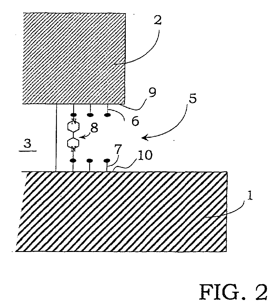
- an undercut 5 of substantially rectangular cross-sectional shape is formed between the peripheral edge of the polysilicon top layer 2 and the substrate 1. It has been thought that the aforementioned organic molecules could fit in this undercut, whose height is controlled by the gate oxidation process to vary between 2 and 100 ⁇ ngströms.
- the layers 1 and 2 will also be referred to as the plates hereinafter.
- the molecules should be anchored with one end in the bottom surface 9 of the top silicon layer 2 (polysilicon) and with the other end in the top surface 10 of the bottom silicon layer 1 (the substrate), as in the even more enlarged view of Figure 2.
- said surfaces should include suitable functional groups to bond to the terminating groups of the molecules.
- the terminating functional groups of the molecules should be prevented from reacting with functional groups in the silicon plate surfaces that lie outside the undercut 5, for otherwise, the molecules would fail to bridge the gap between the plates and function as expected.
- the problem that underlies this invention is solved by a method of controlling and modulating the charge flow through a dielectric oxide of a MOS transistor, wherein the transistor structure comprises a layer of silicon oxide (gate oxide) formed between two silicon plates, with the plates overhanging the silicon oxide layer all around to define an undercut having a substantially rectangular cross-sectional shape and a height of about 3 nm, which method comprises the steps of:
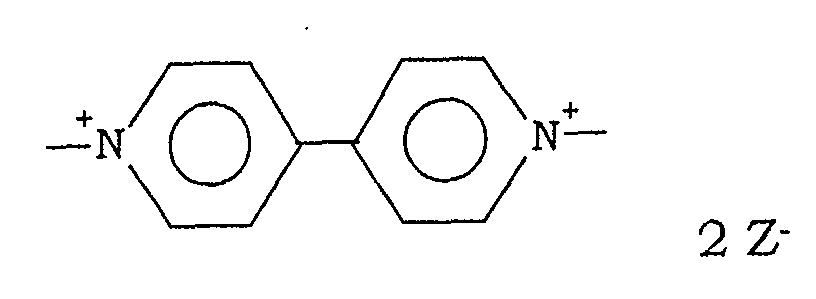
- Said organic molecule has formula R 1 -Y-R 1 , where Y is a redox center having the following formula:
- the structure of a MOS transistor comprises basically a bottom layer or plate 1 and a top layer or plate 2, which plates are separated by a dielectric oxide layer 3.
- the layers 1 and 2 define an undercut 5 in cooperation with the layer 3.
- the first reaction is widely carried out to substitute -OCH 3 groups for the ⁇ OH terminations of glass object surfaces in order to make the glass surface hydrophobic that was originally hydrophilic.
- Such terminations have been used as stoppers in rotaxanes (B. Munn, The New Chemistry, ed. N. Hall (Cambridge University Press, Cambridge), 2000, page 375).
- the second reaction requires external activation (G.P. Lopinski, D.D.M. Wayner, R.A. Wolkow, Nature, 2000, 406 , 48) or a catalyst (F.A. Cotton, G. Wilkinson, Advanced Inorganic Chemistry, 5th Ed., 1988, Wiley, New York, page 1255), in the instance of the molecules being short-chained, but takes place spontaneously in the instance of molecules that, like those used in this invention, have a chain of at least 10 carbon atoms.
- the terminations in the silicon surface need be controlled.
- wet processing under oxidizing conditions e.g. treating with H 2 SO 4 :H 2 O 2 followed by rinsing with water, can be adopted. This process would leave the silicon surface covered with a highly hydroxylated oxide about the thickness of a single layer.
- the native oxide obtained by treating with an aqueous solution of HF may be exposed to a hydrogen atmosphere at moderate temperature for a suitably long time. For example, exposure to H 2 under 30 Pa, at 700°C for 20 minutes, will reduce the amount of oxygen to less than 10 -2 -single layer (T. Ayoama, K. Goto, T. Yamazaki, and T. Ito, J. Vac. Sci. Technol., A 14 , 1996, page 2909).
- the resultant hydrogen-terminated surface is relatively stable, since exposure to air for 10 4 s reveals no appreciable oxidation of the silicon (G.F. Cerofolini, M. Camalleri, C. Galati, S. Lorenti, L. Renna, O. Viscuso, G.G. Condorelli, and I.L. Fragalà, Appl. Phys. Lett. 79 , 2001, page 2378).
- the organic molecule should only anchor itself in the undercut region, not all over the surfaces of the individual silicon plates. Accordingly, the undercut region alone must be provided with suitable terminations for bonding to the molecule.
- the silicon surface of the above MOS transistor structure provided with the undercut is first plasma etched to remove the resist, and then isotropically wet etched using aqueous HF.
- hydrogen terminations should be provided in the surfaces of the undercut region, and oxygenated terminations in the remaining surfaces of the transistor structure.
- the process comprises the following steps:
- hydroxyl terminations should be provided in the surfaces of the undercut region, and hydrogen terminations in the other surfaces.
- the process would include the following steps:
- the invention teaches fabricating a semiconductor electronic device, specifically a FET or a MOSFET, in which an organic molecule is firmly anchored between two opposite surfaces of an undercut provided between two parallel plates 1, 2 of a conductive material (monocrystalline and polycrystalline silicon), with the plates being separated by a layer 3 of dielectric oxide, e.g. a gate oxide or a tunnel oxide.
- the organic molecule 8 can be excited electrically as a Schmitt trigger by applying an electric potential thereto.
Landscapes
- Formation Of Insulating Films (AREA)
- Insulated Gate Type Field-Effect Transistor (AREA)
- Thin Film Transistor (AREA)
- Electroluminescent Light Sources (AREA)
- Semiconductor Memories (AREA)
- Non-Volatile Memory (AREA)
Abstract
Description
Claims (18)
- A method of fabricating a MOS transistor with a controllable and modulatable conduction path through a dielectric gate oxide, the transistor structure comprising a layer (3) of said dielectric oxide formed between two silicon plates (1,2), wherein said silicon plates (1,2) overhang said oxide layer (3) all around to define an undercut (5) having a substantially rectangular cross-sectional shape, said method comprising the steps of:chemically altering the surfaces of said silicon plates (1,2) to have different functional groups (6,7) provided at said undercut (5) from those in the remainder of the surfaces; andselectively reacting said functional groups (6,7) provided at said undercut (5) with an organic molecule (8) having a reversibly reducible center and a molecular length substantially equal to the breadth of said undercut (5), thereby to establish a covalent bond to each end of said organic molecule (8).
- A method according to Claim 1, wherein said organic molecule (8) has formula R1-Y-R1, where Y is a redox center having the following formula:R1 is a -CH2-(CHR2)n-R3 chain, where n=6-8, R2 is H or a C1-C6alkyl group, Z- is a monovalent anion, and R3 is selected from a group that comprises -CH2-CH2-X, -CH=CH2, -C≡CH, and C≡N, where X is either -SH or -SiH2Cl.

- A method according to Claim 2, characterized in that n=7 in said organic molecule (8).
- A method according to Claim 3, characterized in that R2 = H, Z- = Br-, Cl-, F-, I- or PF6 -, and R3 = -CH=CH2, -C≡CH or -CH2-CH2-SiH2Cl in said organic molecule (8).
- A method according to Claim 4, characterized in that n=7, R2 = H, Z- = Br-, and R3 = -CH2-CH2-SiH2Cl or -CH=CH2 or -C≡CH in said organic molecule (8).
- A method according to Claim 2, wherein the surfaces of said silicon plates (1,2) in said undercut (5) are chemically altered to have functional groups (6,7) selected from a group comprising -H, -OH, -Au,-NHnR(2-n), where R = lower alkyl and n = 0, 1, 2.
- A method according to Claim 6, wherein the surfaces of said silicon plates (1,2) in said undercut (5) are chemically altered to have -H functional groups (6,7), whereas said surfaces outside said undercut have -OH functional groups, and wherein R3 = -CH=CH2 or -C≡CH in said organic molecule (8), said method comprising the steps of:a) exposing the surfaces of said plates (1,2), as previously conventionally plasma etched and isotropically etched with aqueous HF, to hydrogen at a high temperature for a sufficiently long time to cleave all of the -OH terminations and hydrogenate the surfaces throughout;b) anisotropically sputtering said plates (1,2) to remove the hydrogen from the surfaces outside the undercut;c) exposing said plates (1,2) to air; andd) exposing said plates (1,2) to a solution of said organic molecule (8).
- A method according to Claim 6, wherein the surfaces of said silicon plates (1,2) in said undercut (5) are chemically altered to have-OH functional groups (6,7), whereas said surfaces outside said undercut have -H functional groups, and wherein R3 = --CH2-CH2-SiH2Cl in said organic molecule (8), said method comprising the steps of:a) exposing the surfaces of said plates (1,2), as previously conventionally plasma etched and isotropically etched with aqueous HF, to oxidation under O2 at a high temperature until oxide as thick as a single layer is obtained;b) anisotropically sputtering said plates (1,2) to remove the oxygen from the surfaces outside the undercut;c) exposing said plates (1,2) to hydrogen at a high temperature for a sufficiently long time to form hydrogen terminations in the surfaces outside the undercut and form hydroxyl terminations in the surfaces of the undercut region; andd) exposing said plates (1,2) to a solution of said organic molecule (8).
- A transistor structure for carrying out the method of Claim 1, which structure comprises a layer (3) of dielectric silicon oxide formed between two silicon plates (1,2), wherein said plates (1,2) overhang said oxide layer (3) all around to define an undercut (5) having a substantially rectangular cross-sectional shape and a preset height, and wherein the surfaces of said plates (1,2) at said undercut (5) have different functional groups (6,7) from those in the other surfaces.
- A transistor structure according to Claim 9, wherein said functional groups (6,7) in the surfaces of said plates (1,2) at said undercut (5) are selected from a group comprising -H, -OH, -Au,-NHnR(2-n), where R = lower alkyl and n = 0, 1, 2.
- A transistor structure according to Claim 10, wherein said functional groups (6,7) in the surfaces of said plates (1,2) at said undercut (5) are either -H or -OH.
- A semiconductor electronic device having a controllable and modulatable conduction path through a dielectric silicon oxide and comprising a layer (3) of said dielectric silicon oxide formed between two silicon plates (1,2), wherein said silicon plates (1,2) overhang said silicon oxide layer (3) all around to define an undercut (5) having a substantially rectangular cross-sectional shape and a preset height, characterized in that an organic molecular moiety (8) is provided within said undercut (5) which contains a reversibly reducible center and whose molecular length substantially equals the width of said undercut (5), said organic molecular moiety (8) being anchored with its ends in opposite surfaces of said undercut (5).
- An electronic device according to Claim 12, wherein said organic molecular moiety (8) is anchored in said opposite surfaces of said undercut (5) by covalent bonds to functional groups (6,7) provided in said opposite surfaces.
- An electronic device according to Claim 13, wherein said organic molecular moiety (8) has formula R1-Y-R1, where Y is a redox center having the following formula:R1 is a -CH2-(CHR2)n-R3' chain, where n=6-8, R2 = H or a C1-C6alkyl group, Z- = monovalent anion, and R3' is selected from a group comprising -CH2-CH2-, -CH2-CH2-Si-, -CH2-CH2-S-, and -CH=CH-.

- An electronic device according to Claim 14, characterized in that n=7, R2 = H, Z- = Br-, Cl-, F-, I- or PF6 -, and R3' = -CH2=CH2-, -CH2-CH2-Si- or -CH=CH- in said organic molecular moiety (8).
- An electronic device according to Claim 14, characterized in that n=7, R2 = H, Z- = Br-, and R3' = -CH2-CH2- or -CH2-CH2-Si- in said organic molecular moiety (8).
- An electronic device according to Claim 12, characterized in that it comprises either a FET or a MOSFET.
- An electronic device according to Claim 12, wherein said organic molecule (8) can be electrically excited as a Schmitt trigger by the application of an electric potential.
Priority Applications (4)
| Application Number | Priority Date | Filing Date | Title |
|---|---|---|---|
| EP01127923A EP1278234B1 (en) | 2001-07-19 | 2001-11-23 | MOS transistor and method of manufacturing |
| JP2002203102A JP4332328B2 (en) | 2001-07-19 | 2002-07-11 | EEPROM having floating gate and method of manufacturing the same |
| US10/199,964 US6724009B2 (en) | 2001-07-19 | 2002-07-18 | Semiconductor integrated electronic device and corresponding manufacturing method |
| US10/763,626 US6890806B2 (en) | 2001-07-19 | 2004-01-23 | Semiconductor integrated electronic device and corresponding manufacturing method |
Applications Claiming Priority (3)
| Application Number | Priority Date | Filing Date | Title |
|---|---|---|---|
| EP01830486 | 2001-07-19 | ||
| EP01830486 | 2001-07-19 | ||
| EP01127923A EP1278234B1 (en) | 2001-07-19 | 2001-11-23 | MOS transistor and method of manufacturing |
Publications (3)
| Publication Number | Publication Date |
|---|---|
| EP1278234A2 true EP1278234A2 (en) | 2003-01-22 |
| EP1278234A3 EP1278234A3 (en) | 2004-04-28 |
| EP1278234B1 EP1278234B1 (en) | 2012-01-11 |
Family
ID=26076773
Family Applications (1)
| Application Number | Title | Priority Date | Filing Date |
|---|---|---|---|
| EP01127923A Expired - Lifetime EP1278234B1 (en) | 2001-07-19 | 2001-11-23 | MOS transistor and method of manufacturing |
Country Status (3)
| Country | Link |
|---|---|
| US (2) | US6724009B2 (en) |
| EP (1) | EP1278234B1 (en) |
| JP (1) | JP4332328B2 (en) |
Cited By (4)
| Publication number | Priority date | Publication date | Assignee | Title |
|---|---|---|---|---|
| EP1630881A1 (en) | 2004-08-31 | 2006-03-01 | STMicroelectronics S.r.l. | Hosting structure of nanometric elements and corresponding manufacturing method |
| EP1630882A1 (en) * | 2004-08-31 | 2006-03-01 | STMicroelectronics S.r.l. | Nanometric structure and corresponding manufacturing method |
| JP2006507660A (en) * | 2002-05-01 | 2006-03-02 | ヒューレット−パッカード デベロップメント カンパニー エル.ピー. | Molecular wire crossbar flash memory |
| US7432120B2 (en) | 2004-08-31 | 2008-10-07 | Stmicroelectronics S.R.L. | Method for realizing a hosting structure of nanometric elements |
Families Citing this family (6)
| Publication number | Priority date | Publication date | Assignee | Title |
|---|---|---|---|---|
| US8362559B2 (en) * | 2002-02-01 | 2013-01-29 | William Marsh Rice University | Hybrid molecular electronic devices containing molecule-functionalized surfaces for switching, memory, and sensor applications and methods for fabricating same |
| US7473947B2 (en) * | 2002-07-12 | 2009-01-06 | Intel Corporation | Process for ultra-thin body SOI devices that incorporate EPI silicon tips and article made thereby |
| JP4723797B2 (en) * | 2003-06-13 | 2011-07-13 | 財団法人国際科学振興財団 | CMOS transistor |
| JP5380481B2 (en) * | 2011-03-07 | 2014-01-08 | 株式会社東芝 | Storage device and manufacturing method thereof |
| JP5781039B2 (en) * | 2012-08-28 | 2015-09-16 | 株式会社東芝 | Method and apparatus for manufacturing functional element |
| JP2015111737A (en) * | 2015-03-06 | 2015-06-18 | 株式会社東芝 | Organic molecular memory |
Family Cites Families (10)
| Publication number | Priority date | Publication date | Assignee | Title |
|---|---|---|---|---|
| US5543356A (en) * | 1993-11-10 | 1996-08-06 | Hitachi, Ltd. | Method of impurity doping into semiconductor |
| EP0926260A3 (en) * | 1997-12-12 | 2001-04-11 | Matsushita Electric Industrial Co., Ltd. | Using antibody - antigen interaction for formation of a patterened metal film |
| US6492695B2 (en) * | 1999-02-16 | 2002-12-10 | Koninklijke Philips Electronics N.V. | Semiconductor arrangement with transistor gate insulator |
| US6459095B1 (en) * | 1999-03-29 | 2002-10-01 | Hewlett-Packard Company | Chemically synthesized and assembled electronics devices |
| US6512119B2 (en) * | 2001-01-12 | 2003-01-28 | Hewlett-Packard Company | Bistable molecular mechanical devices with an appended rotor activated by an electric field for electronic switching, gating and memory applications |
| WO2002080365A1 (en) * | 2001-03-30 | 2002-10-10 | The Penn State Research Foundation | Proton or ion movement assisted molecular devices |
| DE10132640A1 (en) * | 2001-07-05 | 2003-01-23 | Infineon Technologies Ag | Molecular electronics arrangement and method for producing a molecular electronics arrangement |
| US6794220B2 (en) * | 2001-09-05 | 2004-09-21 | Konica Corporation | Organic thin-film semiconductor element and manufacturing method for the same |
| US7074519B2 (en) * | 2001-10-26 | 2006-07-11 | The Regents Of The University Of California | Molehole embedded 3-D crossbar architecture used in electrochemical molecular memory device |
| US6674121B2 (en) * | 2001-12-14 | 2004-01-06 | The Regents Of The University Of California | Method and system for molecular charge storage field effect transistor |
-
2001
- 2001-11-23 EP EP01127923A patent/EP1278234B1/en not_active Expired - Lifetime
-
2002
- 2002-07-11 JP JP2002203102A patent/JP4332328B2/en not_active Expired - Fee Related
- 2002-07-18 US US10/199,964 patent/US6724009B2/en not_active Expired - Lifetime
-
2004
- 2004-01-23 US US10/763,626 patent/US6890806B2/en not_active Expired - Lifetime
Cited By (7)
| Publication number | Priority date | Publication date | Assignee | Title |
|---|---|---|---|---|
| JP2006507660A (en) * | 2002-05-01 | 2006-03-02 | ヒューレット−パッカード デベロップメント カンパニー エル.ピー. | Molecular wire crossbar flash memory |
| EP1630881A1 (en) | 2004-08-31 | 2006-03-01 | STMicroelectronics S.r.l. | Hosting structure of nanometric elements and corresponding manufacturing method |
| EP1630882A1 (en) * | 2004-08-31 | 2006-03-01 | STMicroelectronics S.r.l. | Nanometric structure and corresponding manufacturing method |
| US7432120B2 (en) | 2004-08-31 | 2008-10-07 | Stmicroelectronics S.R.L. | Method for realizing a hosting structure of nanometric elements |
| US7456508B2 (en) | 2004-08-31 | 2008-11-25 | Stmicroelectronics S.R.L. | Hosting structure of nanometric elements and corresponding manufacturing method |
| US7834344B2 (en) | 2004-08-31 | 2010-11-16 | Stmicroelectronics S.R.L. | Nanometric structure and corresponding manufacturing method |
| US7952173B2 (en) | 2004-08-31 | 2011-05-31 | Stmicroelectronics S.R.L. | Nanometric device with a hosting structure of nanometric elements |
Also Published As
| Publication number | Publication date |
|---|---|
| EP1278234B1 (en) | 2012-01-11 |
| EP1278234A3 (en) | 2004-04-28 |
| US6724009B2 (en) | 2004-04-20 |
| US20040152249A1 (en) | 2004-08-05 |
| JP4332328B2 (en) | 2009-09-16 |
| JP2003133551A (en) | 2003-05-09 |
| US6890806B2 (en) | 2005-05-10 |
| US20030049895A1 (en) | 2003-03-13 |
Similar Documents
| Publication | Publication Date | Title |
|---|---|---|
| KR101208785B1 (en) | Floating gate memory device with interpoly charge trapping structure | |
| EP0935293A2 (en) | Nonvolatile semiconductor memory device and method for fabricating the same, and semiconductor integrated circuit device | |
| KR100206985B1 (en) | Flash memory device and manufacturing method thereof | |
| EP1278234B1 (en) | MOS transistor and method of manufacturing | |
| US20070200168A1 (en) | MONOS type nonvolatile memory cell, nonvolatile memory, and manufacturing method thereof | |
| US6127229A (en) | Process of forming an EEPROM device having a split gate | |
| CN102543885A (en) | Split-gate memory device and forming method thereof | |
| JPH05235368A (en) | Erasing of data | |
| US6180977B1 (en) | Self-aligned edge implanted cell to reduce leakage current and improve program speed in split-gate flash | |
| KR20060093914A (en) | Split type flash memory device having self-aligned control gate and manufacturing method thereof | |
| EP1293987A1 (en) | Nonvolatile semiconductor memory device and method of manufacturing the same | |
| CN101814322A (en) | Operation method of non-volatile memory cell and memory device using the method | |
| CN1885508A (en) | Flash memory process | |
| CN1202981A (en) | Method for producing very small structural widths on a semiconductor substrate | |
| JP2842169B2 (en) | Nonvolatile semiconductor memory device | |
| KR20050069149A (en) | Semiconductor device and fabricating method thereof | |
| KR20100078498A (en) | Non-volatile memory device and the method for fabricating the same | |
| KR100310424B1 (en) | A method of fabricating a semiconductor device | |
| KR19990007264A (en) | Semiconductor memory device and manufacturing method thereof | |
| KR100281117B1 (en) | Ipyrom element and its manufacturing method | |
| TW400655B (en) | The method of forming the spacer on the peripheral of the lower portion of the floating gate in split gate type flash memory | |
| KR100657151B1 (en) | Nonvolatile Memory Device and Manufacturing Method Thereof | |
| Carvalho et al. | Effect of Gate Capacitance Ratio on Ion-Sensitive Fet Memory | |
| KR20090110806A (en) | Floating Gate Memory Device with Interpoly Charge Trapping Structure | |
| KR20050100058A (en) | Split-gate type non-volatile memory device and method of fabricating the same |
Legal Events
| Date | Code | Title | Description |
|---|---|---|---|
| PUAI | Public reference made under article 153(3) epc to a published international application that has entered the european phase |
Free format text: ORIGINAL CODE: 0009012 |
|
| AK | Designated contracting states |
Kind code of ref document: A2 Designated state(s): AT BE CH CY DE DK ES FI FR GB GR IE IT LI LU MC NL PT SE TR |
|
| AX | Request for extension of the european patent |
Free format text: AL;LT;LV;MK;RO;SI |
|
| PUAL | Search report despatched |
Free format text: ORIGINAL CODE: 0009013 |
|
| AK | Designated contracting states |
Kind code of ref document: A3 Designated state(s): AT BE CH CY DE DK ES FI FR GB GR IE IT LI LU MC NL PT SE TR |
|
| AX | Request for extension of the european patent |
Extension state: AL LT LV MK RO SI |
|
| RIC1 | Information provided on ipc code assigned before grant |
Ipc: 7H 01L 21/28 A Ipc: 7H 01L 29/51 B Ipc: 7H 01L 51/20 B |
|
| 17P | Request for examination filed |
Effective date: 20041025 |
|
| AKX | Designation fees paid |
Designated state(s): DE FR GB IT |
|
| 17Q | First examination report despatched |
Effective date: 20080609 |
|
| RAP1 | Party data changed (applicant data changed or rights of an application transferred) |
Owner name: STMICROELECTRONICS SRL |
|
| GRAP | Despatch of communication of intention to grant a patent |
Free format text: ORIGINAL CODE: EPIDOSNIGR1 |
|
| RIC1 | Information provided on ipc code assigned before grant |
Ipc: H01L 29/51 20060101ALI20110617BHEP Ipc: H01L 21/28 20060101AFI20110617BHEP |
|
| GRAS | Grant fee paid |
Free format text: ORIGINAL CODE: EPIDOSNIGR3 |
|
| GRAA | (expected) grant |
Free format text: ORIGINAL CODE: 0009210 |
|
| AK | Designated contracting states |
Kind code of ref document: B1 Designated state(s): DE FR GB IT |
|
| REG | Reference to a national code |
Ref country code: GB Ref legal event code: FG4D |
|
| REG | Reference to a national code |
Ref country code: DE Ref legal event code: R096 Ref document number: 60145924 Country of ref document: DE Effective date: 20120308 |
|
| RAP2 | Party data changed (patent owner data changed or rights of a patent transferred) |
Owner name: STMICROELECTRONICS SRL |
|
| PLBE | No opposition filed within time limit |
Free format text: ORIGINAL CODE: 0009261 |
|
| STAA | Information on the status of an ep patent application or granted ep patent |
Free format text: STATUS: NO OPPOSITION FILED WITHIN TIME LIMIT |
|
| PG25 | Lapsed in a contracting state [announced via postgrant information from national office to epo] |
Ref country code: IT Free format text: LAPSE BECAUSE OF FAILURE TO SUBMIT A TRANSLATION OF THE DESCRIPTION OR TO PAY THE FEE WITHIN THE PRESCRIBED TIME-LIMIT Effective date: 20120111 |
|
| 26N | No opposition filed |
Effective date: 20121012 |
|
| REG | Reference to a national code |
Ref country code: DE Ref legal event code: R097 Ref document number: 60145924 Country of ref document: DE Effective date: 20121012 |
|
| PGFP | Annual fee paid to national office [announced via postgrant information from national office to epo] |
Ref country code: FR Payment date: 20130107 Year of fee payment: 12 |
|
| GBPC | Gb: european patent ceased through non-payment of renewal fee |
Effective date: 20121123 |
|
| PG25 | Lapsed in a contracting state [announced via postgrant information from national office to epo] |
Ref country code: GB Free format text: LAPSE BECAUSE OF NON-PAYMENT OF DUE FEES Effective date: 20121123 |
|
| REG | Reference to a national code |
Ref country code: FR Ref legal event code: ST Effective date: 20140731 |
|
| PG25 | Lapsed in a contracting state [announced via postgrant information from national office to epo] |
Ref country code: FR Free format text: LAPSE BECAUSE OF NON-PAYMENT OF DUE FEES Effective date: 20131202 |
|
| REG | Reference to a national code |
Ref country code: DE Ref legal event code: R082 Ref document number: 60145924 Country of ref document: DE Representative=s name: SCHMITT-NILSON SCHRAUD WAIBEL WOHLFROM PATENTA, DE |
|
| PGFP | Annual fee paid to national office [announced via postgrant information from national office to epo] |
Ref country code: DE Payment date: 20201020 Year of fee payment: 20 |
|
| REG | Reference to a national code |
Ref country code: DE Ref legal event code: R071 Ref document number: 60145924 Country of ref document: DE |