EP1277112B1 - Erfassung eines regeisterwertes zu einem anderen taktbereich - Google Patents
Erfassung eines regeisterwertes zu einem anderen taktbereich Download PDFInfo
- Publication number
- EP1277112B1 EP1277112B1 EP01928878A EP01928878A EP1277112B1 EP 1277112 B1 EP1277112 B1 EP 1277112B1 EP 01928878 A EP01928878 A EP 01928878A EP 01928878 A EP01928878 A EP 01928878A EP 1277112 B1 EP1277112 B1 EP 1277112B1
- Authority
- EP
- European Patent Office
- Prior art keywords
- signal
- register
- shift
- address
- recited
- Prior art date
- Legal status (The legal status is an assumption and is not a legal conclusion. Google has not performed a legal analysis and makes no representation as to the accuracy of the status listed.)
- Expired - Lifetime
Links
Images


Classifications
-
- G—PHYSICS
- G01—MEASURING; TESTING
- G01R—MEASURING ELECTRIC VARIABLES; MEASURING MAGNETIC VARIABLES
- G01R31/00—Arrangements for testing electric properties; Arrangements for locating electric faults; Arrangements for electrical testing characterised by what is being tested not provided for elsewhere
- G01R31/28—Testing of electronic circuits, e.g. by signal tracer
- G01R31/317—Testing of digital circuits
- G01R31/31725—Timing aspects, e.g. clock distribution, skew, propagation delay
-
- G—PHYSICS
- G06—COMPUTING OR CALCULATING; COUNTING
- G06F—ELECTRIC DIGITAL DATA PROCESSING
- G06F5/00—Methods or arrangements for data conversion without changing the order or content of the data handled
- G06F5/06—Methods or arrangements for data conversion without changing the order or content of the data handled for changing the speed of data flow, i.e. speed regularising or timing, e.g. delay lines, FIFO buffers; over- or underrun control therefor
-
- G—PHYSICS
- G01—MEASURING; TESTING
- G01R—MEASURING ELECTRIC VARIABLES; MEASURING MAGNETIC VARIABLES
- G01R31/00—Arrangements for testing electric properties; Arrangements for locating electric faults; Arrangements for electrical testing characterised by what is being tested not provided for elsewhere
- G01R31/28—Testing of electronic circuits, e.g. by signal tracer
- G01R31/317—Testing of digital circuits
- G01R31/3181—Functional testing
- G01R31/3185—Reconfiguring for testing, e.g. LSSD, partitioning
- G01R31/318533—Reconfiguring for testing, e.g. LSSD, partitioning using scanning techniques, e.g. LSSD, Boundary Scan, JTAG
- G01R31/318594—Timing aspects
Definitions
- This invention is related to the field of electronic circuits and, more particularly, to capturing a register value to another clock domain within an integrated circuit.
- Integrated circuits typically include test circuitry used to allow testing of the integrated circuits at manufacturing time or even in a system with other integrated circuits.
- the test access port defined by the Joint Test Access Group (JTAG) and later refined into Institute of Electrical and Electronics Engineers (IEEE) standard 1149.1 is a popular test circuit.
- the JTAG TAP typically operates at a relatively low clock frequency (e.g. 10 MHz).
- the other circuitry within the integrated circuit may operate at a significantly higher frequency (e.g. 33 MHz to approximately 1 GHz is possible today, and higher frequencies than 1 GHz are expected in the future).
- the JTAG TAP is said to be in a first clock domain and the other circuitry in the integrated circuit is said to be in a second clock domain different than the first.
- the test involves transferring a value from a register in the second clock domain to a register in the first clock domain. Since the clocks are of different frequencies (and/or may have phase differences with respect to each other or no phase relationship at all), the transfer must be synchronized in some fashion. This transfer may be particularly problematic if the value to be transferred is changing at the time the value is being transferred. For example, a register in the first clock domain may be configured to receive a multi-bit register value from the second clock domain one bit at a time.
- the multi-bit register value is changing during the synchronization, some bits of the multi-bit value may reflect the value prior to the change, and other bits of the multi-bit value may reflect the value subsequent to the change. Thus, the resulting multi-bit value in the first clock domain may be inaccurate. Even if the multi-bit value is synchronized in parallel, some of the bits may synchronize on one clock of the first clock domain and other bits may synchronize on another clock. Thus, the synchronized value in the first clock domain may not reflect the state of the multi-bit value.
- EP-A-0 798 630 describes a method and circuit for transferring data between clock domains having first and second clock signals at different rates. Data is received and provided in holding registers at a first clock rate. Data is synchronized in the holding registers then transferred to the sampling registers at the second clock rate. The data is read in the sampling registers at the second clock rate.
- An aspect of the invention provides an apparatus according to claim 1. Another aspect of the invention provides a method according to claim 16.
- the problems outlined above are in large part solved by an integrated circuit as described herein.
- the integrated circuit includes an address register, clocked by the clock signal corresponding to the TAP and thus in a first clock domain, used to address a control/status register within the integrated circuit.
- the address register receives a signal indicating that an address is to be loaded into the address register.
- a control circuit is coupled to receive the signal and to generate a second signal responsive to the address register being loaded.
- the control register may generate the second signal after the address register has stabilized for observation in a second clock domain corresponding to the clock signal of the integrated circuit.
- a shadow register clocked by the clock signal of the integrated circuit and thus in the second clock domain, is coupled to receive the second signal and to load a value from the control/status register addressed by the address loaded into the address register responsive to the second signal. In this manner, a valid value from the addressed register is synchronized in the second clock domain.
- the value for the shadow register may subsequently be synchronized into the first clock domain (of the TAP), and subsequently transferred out of the integrated circuit via the test interface.
- a similar sequence may be performed for a write from the TAP to a control/status register. More particularly, the control circuit may receive the signal indicating that an address is loaded into the address register and may generate a second signal to select the addressed control/status register in response to the signal (after the address register is stabilized for observation in the second clock domain). Similarly, the control circuit may receive a third signal indicating that the data to be written is loaded into a data register (in the first clock domain) and may generate a fourth signal in response to the third signal (after the data register is stabilized for observation in the second clock domain). In response to the fourth signal, the data may be loaded into the selected control/status register.
- integrated circuit 10 includes a JTAG TAP controller 12 (which includes an instruction register (IR) 14 specified by the IEEE 1149.1 specification), an address register 16, a data register 18, a shadow register 20, a plurality of control/status registers (CSRs) 22A-22E, a CSR access control circuit 24, and a CSR mux 26.
- JTAG TAP controller 12 is coupled to a test interface and is further coupled to address register 16, data register 18, and CSR access control circuit 24.
- the test interface comprises various inputs and outputs to the test TAP controller 12 and circuitry.
- the test interface is the JTAG test interface including a clock signal (TCK) on line 28, a test data out (TDO) signal on line 30, a test data in signal (TDI) on line 32, and a test mode select (TMS) signal on line 34.
- the interface may also include a reset signal (TRST) (not shown).
- Address register 16 is coupled to CSR access control circuit 24 and is clocked by the TCK clock signal, and may also be coupled to receive the TDI signal.
- Data register 18 is coupled to shadow register 18 and is clocked by the TCK signal as well.
- CSR access control circuit 24 is coupled to receive a clock signal CLK on line 36.
- shadow register 20 and CSRs 22A-22E are clocked by the clock signal CLK (connections to CSRs 22A-22E not shown in Fig. 1). While the connection of shadow register 20 to line 36 is shown separate from the connection to CSR access control circuit 24 for clarity in the drawing, the clock signal CLK may generally be routed to shadow register 20 within integrated circuit 10.
- CSR access control circuit 24 is further coupled to CSR mux 26 and shadow register 20.
- Shadow register 20 is coupled to receive an output of CSR mux 26, which is further coupled to each of CSRs 22A-22E as inputs.
- the frequency of the CLK clock signal may generally be greater than the frequency of the TCK clock signal.
- the TCK clock signal may generally operate at a frequency of approximately 10 MHz, while the CLK clock signal may operate at any other frequency.
- the CLK clock signal may have a frequency in the range of 33 MHz to 1 GHz or more.
- the frequency of the CLK clock signal may be greater than the frequency of the TCK clock signal.
- each of CSRs 22A-22E is scannable via the test interface.
- each of the CSRs 22A-22E may be selected, via signal combinations on the test interface, to provide its current value on the test interface. In this manner, observability to the internal state of integrated circuit 10 may be achieved.
- each of the CSRs 22A-22E may be assigned an address that uniquely identifies that CSR among the CSRs 22A-22E.
- Signal combinations on the test interface may be used to provide an address in address register 16 which identifies one of the CSRs 22A-22E.
- An internal signal (Shift_AR in Fig. 1) may be asserted by TAP controller 12 to indicate that address register 16 is to load the address provided on the test interface.
- the same signal may be applied to CSR access control circuit 24, ultimately causing the value in the identified CSR to be loaded into shadow register 20 responsive to the signal.
- the CSR access control circuit 24 may include a decoder that decodes the address and selects the CSR Then the CSR may be loaded into shadow register 20 after the address register has stabilized for observation in the CLK clock domain. Subsequently, the value in shadow register 20 may be loaded into data register 18, thus transferring the value into the clock domain of the TCK clock signal. More particularly, the data may be transferred into the data register 18 after the data in the shadow register 20 has stabilized for observation in the TCK clock domain. Additional commands on the test interface may be used to scan the data out of data register 18 onto the test interface, and thus the value of the selected CSR may be observed on the test interface.
- each of the bits stored in the CSR is concurrently synchronized in the clock domain of the CSR (i.e. the CLK clock domain).
- a valid value is captured, and later transferred to the clock domain of the JTAG TAP (i.e. the TCK clock domain).
- the bits stored in the CSR are concurrently loaded into shadow register 20 in the clock domain of the CSR, even CSRs which are frequently changing (e.g. a counter which changes every period or every N periods) may be validly observed via the test interface.
- Each CSR 22A-22E may store a portion of the state of integrated circuit 10.
- Various circuitry within integrated circuit 10 may use the values in the CSRs 22A-22E to determine the operation of the circuitry and/or to report status of the circuitry in operation.
- the address is shifted into the address register 16 from the test interface.
- JTAG TAP controller 12 upon determining that the test interface is providing an address, may assert the Shift_AR signal coupled to address register 16.
- the Shift_AR signal may remain asserted until each bit of the address has been shifted into address register, and may then be deasserted. While the Shift_AR signal is asserted, address register 16 shifts in input bits from the TDI signal. Address register 16 ceases shifting when the Shift_AR signal is deasserted.
- CSR access control circuit 24 receives the Shift_AR signal and may determine that the address register has been loaded by detecting the deassertion transition (from asserted to deasserted) of the Shift_AR signal.
- CSR access control circuit 24 may synchronize the Shift_AR signal into the CLK clock domain. More particularly, CSR access control circuit 24 may "dual rank synchronize" the Shift_AR signal and may detect the deassertion of the Shift_AR signal by examining the dual rank synchronized signal.
- a signal is dual ranked synchronized into a clock domain if the signal has been passed through at least a pair of clocked storage devices (e.g. flops, registers, latches, etc.) clocked by the clock signal defining that clock domain. If the signal is stable after each transition for at least 2 clock periods of the clock signal, dual rank synchronization may be used to detect each transition.
- CSR access control circuit 24 may delay N CLK clock periods from detecting the transition before it uses the address in order to allow the address to stabilize in the CLK clock domain.
- the number of clock periods of delay may be based, in part, on the ratio of the frequency of the CLK clock signal to the frequency of the TCK clock signal.
- the delay may be a number of CLK clock periods greater than or equal to the ratio, allowing a clock period of the TCK clock to expire from the transition of the Shift_AR signal to the use of the address.
- the delay may be a number of CLK clock periods greater than or equal to twice the ratio, allowing for two clock periods of the TCK clock to expire.
- CSR access control circuit 24 decodes the address from address register 16 and provides select controls to CSR mux 26 to select the addressed CSR 22A-22E. In this manner, the value stored in the addressed CSR 22A-22E may be provided as an input to shadow register 20. CSR access control circuit 24 may then assert the Shadow_Load signal to shadow register 20 to cause shadow register 20 to load the input.
- Shadow register 20 may be physically located within integrated circuit 10 at any convenient place (e.g. not physically near data register 18), since the interconnect between the two registers is limited.
- shadow register 20 may receive the TCK clock signal and may control shifting using the TCK clock signal.
- the parallel load from mux 26 may be controlled by the CLK clock signal.
- shadow register 20 may not receive the TCK clock signal.
- shadow register 20 may load the input (the value from the addressed CSR 22A-22E) well before the value is shifted into the data register (e.g. at least several clock periods of the TCK clock signal).
- the value at the output of shadow register 20 may be stable prior to transferring the value to data register 18 and thus the data need not be explicitly synchronized. However, this synchronization could be implemented, if desired.
- a register is loaded if the value at the input of the register is stored into the register and retained by the register during the succeeding clock period.
- the register provides a value loaded into the register at its output subsequent to being loaded.
- the test interface is the JTAG test interface including the TMS, TDI, and TDO signals.
- the TDI signal is used to shift bits of data into integrated circuit 10
- the TDO signal is used to shift bits of data out of integrated circuit 10, at a maximum rate of one bit per TCK clock period.
- the TMS signal is used to select test modes, and cycles the JTAG TAP controller 12 through the TAP state machine defined by the IEEE 1449.1 specification. It is noted that various signal combinations may be used to cause the desired behavior in JTAG TAP controller 12.
- a signal combination may be one or more TCK periods of signal assertions and deassertions on the TMS and TDI signals as defined in the IEEE 1149.1 specification.
- JTAG TAP controller 12 includes instruction register 14, into which instructions may be shifted using the TDI input signal.
- the IEEE 1449.1 specification defines three mandatory instructions (EXTEST, SAMPLE/PRELOAD, and BYPASS).
- JTAG TAP controller 12 may support one or more additional instructions, such as an address load instruction and a data load instruction described herein.
- JTAG TAP controller 12 may load the next M bits transmitted on the TDI signal into address register 16 (where M is the number of bits in address register 16, which may be at least enough bits to specify an address for each of the CSRs).
- the JTAG TAP controller 12 may assert the Shift_AR signal to address register 16, which may then receive the TDI signal as a shift-in input Thus, over the next M clock periods of the TCK clock signal, bits transmitted on the TDI signal are shifted into address register 16.
- JTAG TAP controller 12 may ensure sufficient delay has occurred to stabilize the shadow register data value in the TCK clock domain and may assert the Shift_D signal for a number of TCK clock periods equal to the number of bits in data register 18.
- the delay to ensure stability of the shadow register data value may occur inherently due to the longer clock period of the TCK clock signal and the shifting of the instruction into the IR register 14.
- a sequence of signal combinations on the JTAG interface to read a value of a CSR may include signal combinations shifting the address load instruction into the instruction register, followed by the shifting of the address of the CSR to be read into address register 16, followed by shifting the data load instruction into the instruction register 14, followed by shifting the transfer to DR instruction into the instruction register, followed by shifting data from the DR register 13 onto the TDO signal.
- test interface is used as the test interface
- any suitable test interface could be used in alternative embodiments.
- the above method for addressing a register in a first clock domain from a second clock domain, using the signal indicating that the address register is loaded to load a shadow register with the value in the addressed register may be used for any two clock domains, even if circuitry in the two domains is not being used for testing purposes.
- Fig. 1 illustrates one shadow register 20
- multiple shadow registers could be used.
- a shadow register could be included for each CSR, if desired.
- an integrated circuit having two or more clock domains in addition to the TCK clock domain may employ the above method.
- each of the clock domains other than the TCK clock domain could employ a CSR access control circuit and a shadow register as described above.
- a single CSR access control circuit may be used, designed for the worst case delay of the various clock domains.
- the CSR access control circuit 24 may receive the Shift_AR signal and may generate a second signal to select the addressed CSR 22A-22E in response to the Shift_AR signal (after the address register is stabilized for observation in the second clock domain).
- the CSR access control circuit may receive the Shift_DR signal and may generate a CSR load signal to the selected CSR 22A-22E in response to the deassertion transition of the Shift_DR signal (after the data register 18 is stabilized for observation in the CLK clock domain).
- the data may be loaded into the selected control/status register.
- Dotted lines from the Shift_DR signal to CSR access control circuit 24, from CSR access control circuit 24 to each CSR 22A-22E (for the control signal for each CSR to load the data from data register 18), and from data register 18 to each CSR 22A-22E (to provide the data from data register 18 as an input) illustrate exemplary connections for performing writes to CSRs.
- Each CSR 22A-22E may receive a separate control signal from CSR access control circuit 24, and CSR access control circuit 24 may assert one of the signals responsive to decoding the address from the address register to cause the selected CSR 22A-22 to update with the data from data register 18.
- each bit of the address register 16 and/or data register 18 may be parallel loaded and the signal to load could be a pulse.
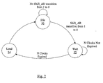
- Fig. 2 a state machine diagram of an exemplary state machine that may be employed in one embodiment of CSR access control circuit 24 is shown. Other embodiments are possible and contemplated.
- the state machine includes an idle state 50, a wait state 52, and a load state 54.
- CSR access control circuit 24 In idle state 50, CSR access control circuit 24 is not preparing to load data corresponding to an addressed CSR into shadow register 20.
- the state machine remains in idle state 50 if no deassertion transition on the Shift_AR signal is detected. If a deassertion transition on the Shift_AR signal is detected, the state machine transitions to wait state 52.
- CSR access control circuit 24 waits for N clock periods to expire, in order to allow the address in address register 16 to stabilize (as described above). Thus, the state machine remains in wait state 52 if N clock periods have not expired and transitions to load state 54 if N clock periods have expired.
- CSR access control circuit 24 decodes the address from address register 16 and asserts select control signals to CSR mux 26, and asserts the Shadow_Load signal. The state machine then returns to idle state 50.
- CSR access control circuit 24 may decodes the address from address register 16 and asserts a CSR_Load signal to the selected CSR.
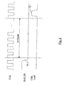
- a timing diagram is shown illustrating the CLK clock signal, the Shift_AR signal, and the Shadow_Load signal according to one embodiment of CSR access control circuit 24.
- the Shift_AR signal transitions to a logic low (which may represent deassertion) (reference numeral 60).
- the Shift_AR signal shown in Fig. 3 may represent the dual rank synchronized output of the Shift_AR signal. Since the transition has been detected, CSR access control circuit 24 begins counting the N clock periods of delay prior to decoding the address and asserting the Shadow_Load signal.
- the N clock periods of delay may be represented in Fig. 3 as the distance between the two vertical dashed lines.
- CSR access control circuit 24 pulse the Shadow_Load signal (reference numeral 62) to cause shadow register 24 to capture the value of the addressed CSR.
- a similar timing diagram with the Shift_DR signal 70 and N clock periods of delay to asserting the control signal (CSR_load) from CSR access control circuit 24 to the addressed CSR 22A-22E to update with the data from the data register is illustrated in Fig. 4.
- the CSR_load signal is pulsed after the N clock periods of delay (reference numeral 72).
- the deassertion transition of the Shift_AR signal is illustrated as a transition from a logical 1 to a logical 0, or from a high to a low.
- a signal may be defined to be asserted at a low value and deasserted at a high value, if desired.
- responsive means that the event being responded to (e.g. a signal assertion or generation, etc.) is a condition precedent to the response.
- the response may be either indirectly or directly caused by the event being responded to.
Landscapes
- Engineering & Computer Science (AREA)
- Physics & Mathematics (AREA)
- General Engineering & Computer Science (AREA)
- General Physics & Mathematics (AREA)
- Theoretical Computer Science (AREA)
- Tests Of Electronic Circuits (AREA)
- Time-Division Multiplex Systems (AREA)
- Synchronisation In Digital Transmission Systems (AREA)
- Stabilization Of Oscillater, Synchronisation, Frequency Synthesizers (AREA)
- Radar Systems Or Details Thereof (AREA)
- Test And Diagnosis Of Digital Computers (AREA)
Claims (22)
- Vorrichtung, die aufweist:ein Adressenregister (16), das dafür ausgelegt ist, eine Adresse zu speichern, die ein erstes Register (22A) aus einer Mehrzahl von Registern (22A-22E) anzeigt, wobei das Adreßregister (16) so angeschlossen ist, daß es ein erstes Signal (Shift_AR) zum Laden der Adresse in das Adreßregister (16) empfängt, und wobei das Adreßregister (16) von einem ersten Taktsignal (28) getaktet wird, und wobei das erste Register (22A) von einem zweiten Taktsignal (36), das verschieden von dem ersten Taktsignal (28) ist, getaktet wird; undeinen Steuerschaltkreis (24), der so angeschlossen ist, daß er das erste Signal (Shift_AR) empfängt, wobei der Steuerschaltkreis (24) so eingerichtet ist, daß er die Adresse als Antwort auf das erste Signal (Shift_AR) verwendet, um das erste Register (22A) auszuwählen.
- Vorrichtung nach Anspruch 1, dadurch gekennzeichnet, daß der Steuerschaltkreis (24) eingerichtet ist, um die Adresse nach Verzögerung um N Taktperioden des zweiten Taktsignals (36) nach dem Empfangen des ersten Signals (Shift_AR) zu verwenden, wobei N eine positive ganze Zahl ist.
- Vorrichtung nach Anspruch 2, dadurch gekennzeichnet, daß sie darüber hinaus ein Datenregister (18) aufweist, das von dem ersten Taktsignal (28) getaktet wird, wobei das Datenregister (18) so angeschlossen ist, daß es ein zweites Signal (Shift_D) zum Laden von Daten in das Datenregister (18) empfängt, und wobei der Steuerschaltkreis (24) so angeschlossen ist, daß er das zweite Signal (Shift_D) mpfängt und das erste Register (22A) veranlaßt, sich als Antwort auf das zweite Signal (Shift_D) mit den Daten zu aktualisieren.
- Vorrichtung nach Anspruch 3, dadurch gekennzeichnet, daß der Steuerschaltkreis (24) so eingerichtet ist, daß er das erste Register (22A) veranlaßt, sich nach einer Verzögerung von N Taktperioden des zweiten Taktsignals (36) nach dem Empfangen des zweiten Signals (Shift_D) zu aktualisieren, wobei N eine positive ganze Zahl ist.
- Vorrichtung nach Anspruch 1, dadurch gekennzeichnet, daß sie darüber hinaus ein Datenregister (18) aufweist, das eingerichtet ist, um einen Inhalt des ersten Registers (22A) als Antwort auf das Auswählen des ersten Registers (22A) durch den Steuerschaltkreis (24) zu empfangen.
- Vorrichtung nach Anspruch 5, dadurch gekennzeichnet, daß das Datenregister (18) von den ersten Taktsignalen (28) getaktet wird.
- Vorrichtung nach Anspruch 5, dadurch gekennzeichnet, daß das Datenregister (18) so angeschlossen ist, daß es ein zweites Signal (Shift_D) zum Laden von Daten in das Datenregister (18) empfängt und daß der Steuerschaltkreis (24) so angeschlossen ist, daß er das zweite Signal (Shift_D) empfängt und so eingerichtet ist, daß er das erste Register (22A) veranlasst, sich mit den geladenen Daten als Antwort auf das zweite Signal (Shift_D) zu aktualisieren.
- Vorrichtung nach Anspruch 1, dadurch gekennzeichnet, daß sie darüber hinaus aufweist:ein zweites Register (20), das so angeschlossen ist, daß es einen Wert, der in dem ersten Register (22A) gespeichert ist, empfängt, wobei das zweite Register (20) durch das zweite Taktsignal (36) getaktet wird; undder Steuerschaltkreis (24) so eingerichtet ist, daß er ein zweites Signal (Shadow_Load) als Antwort auf das erste Signal (Shift_AR) erzeugt und wobei das zweite Register (20) so angeschlossen ist, daß es das zweite Signal (Shadow_Load) empfängt und den Wert als Antwort auf das zweite Signal (Shadow_Load) lädt.
- Vorrichtung nach Anspruch 8, dadurch gekennzeichnet, daß der Steuerschaltkreis (24) so eingerichtet ist, daß er das zweite Signal (Shadow_Load) als Antwort darauf erzeugt, daß das erste Signal (Shift_AR) anzeigt, daß die Adresse in das Adreßregister (16) geladen wurde.
- Vorrichtung nach Anspruch 9, dadurch gekennzeichnet, daß der Steuerschaltkreis (24) so eingerichtet ist, daß er: (i) ein oder mehrere Taktperioden des zweiten Taktsignals (36) ab dem ersten Signal (Shift_AR) verzögert, das anzeigt, daß die Adresse in das Adreßregister (16) geladen wurde und dann (ii) das zweite Signal (Shadow_Load) generiert, um das zweite Register zu veranlassen, den Wert zu laden.
- Vorrichtung nach Anspruch 9, dadurch gekennzeichnet, daß das erste Signal (Shift_AR) ein Verschiebesignal ist und daß das Verschiebesignal anzeigt, daß das Adreßregister (16) geladen wird durch einen Übergang von dem Verschiebezustand in einen Nicht-Verschiebezustand.
- Vorrichtung nach Anspruch 11, dadurch gekennzeichnet, daß der Steuerschaltkreis (24) so eingerichtet ist, daß er das Verschiebesignal in zwei Ebenen synchronisiert, um das zweite Signal (Shadow_Load) zu generieren.
- Vorrichtung nach Anspruch 8, dadurch gekennzeichnet, daß sie zusätzlich einen Multiplexer (26) aufweist, der an jedes aus der Mehrzahl von Registern (22A-22E) so angeschlossen ist, daß er Werte, die in Ihnen gespeichert sind, empfängt und der darüber hinaus so an den Steuerschaltkreis (24) angeschlossen ist, daß er ein oder mehrere ausgewählte Steuersignale empfängt und wobei der Steuerschaltkreis (24) so angeschlossen ist, daß er die Adresse empfängt und die Adresse decodiert, um die ausgewählten Steuersignale zu generieren.
- Vorrichtung nach Anspruch 8, dadurch gekennzeichnet, daß sie darüber hinaus einen zweiten Steuerschaltkreis (12) aufweist, der an eine Testschnittstelle (28-34) angeschlossen ist, wobei der zweite Steuerschaltkreis (12) so eingerichtet ist, daß er das erste Signal (Shift_AR) als Antwort auf einen oder mehrere Befehle generiert, die von der Testschnittstelle (28-34) empfangen wurden.
- Vorrichtung nach Anspruch 14, dadurch gekennzeichnet, daß die Testschnittstelle (28-34) kompatibel ist mit dem Joint Test Access Group (JTAG) Testzugangsanschluß (test access port, TAP).
- Verfahren, das aufweist:Laden eines Adreßregisters (16) mit einer Adresse, die ein erstes Register (22A) aus einer Mehrzahl von Registern (22A-22E) anzeigt, wobei das Adreßregister (16) von einem ersten Taktsignal (28) getaktet wird, und wobei das erste Register (22A) von einem zweiten Taktsignal (36) getaktet wird, das verschieden von dem ersten Taktsignal (28) ist und wobei das Laden des Adreßregisters (16) von einem ersten Signal (Shift_AR) gesteuert wird, das von dem Adreßregister (16) empfangen wird; undVerwenden der Adresse, um das erste Register (22A) als Antwort auf das erste Signal (Shift_AR) auszuwählen.
- Verfahren nach Anspruch 16, dadurch gekennzeichnet, daß es darüber hinaus aufweist:Laden eines Wertes, der in dem ersten Register (22A) gespeichert ist, in ein zweites Register (20) als Antwort auf das Laden des ersten Adreßregisters (16), wobei das zweite Register (20) von einem zweiten Taktsignal (36) getaktet wird, das verschieden von dem ersten Taktsignal (28) ist.
- Verfahren nach Anspruch 17, dadurch gekennzeichnet, daß das erste Signal (Shift_AR) ein Verschiebesignal ist und daß das Laden des Wertes als Antwort auf das Verschiebesignal, das den Übergang von einem Verschiebezustand in einen Nicht-Verschiebezustand schafft, erfolgt.
- Verfahren nach Anspruch 18, dadurch gekennzeichnet, daß das Laden des Wertes um eine oder mehrere Taktperioden des zweiten Taktsignals (36) verzögert wird.
- Verfahren nach Anspruch 17, dadurch gekennzeichnet, daß das Laden des Wertes eine Zwei-Ebenen-Synchronisation des ersten Signals (Shift_AR) in eine Taktdomäne des zweiten Taktsignals (36) aufweist.
- Verfahren nach Anspruch 17, dadurch gekennzeichnet, daß das Laden des Wertes aufweist:Decodieren der Adresse; undAuswahl des ersten Registers (22A) aus der Mehrzahl von Registern (22A-22E), um den Wert in das zweite Register (20) einzugeben, wobei die Auswahl als Antwort auf das Decodieren erfolgt.
- Verfahren nach Anspruch 17, dadurch gekennzeichnet, daß es darüber hinaus ein Generieren des ersten Signals (Shift_AR) als Antwort auf einen oder mehrere Befehle aufweist, die von einer Testschnittstelle (28-34) empfangen wurden.
Applications Claiming Priority (3)
| Application Number | Priority Date | Filing Date | Title |
|---|---|---|---|
| US09/557,987 US6681337B1 (en) | 2000-04-25 | 2000-04-25 | Method and apparatus for loading data from an address specified by an address register into a different register wherein the registers are clocked in different time domains |
| US557987 | 2000-04-25 | ||
| PCT/US2001/013397 WO2001082081A2 (en) | 2000-04-25 | 2001-04-25 | Capturing of a register value to another clock domain |
Publications (2)
| Publication Number | Publication Date |
|---|---|
| EP1277112A2 EP1277112A2 (de) | 2003-01-22 |
| EP1277112B1 true EP1277112B1 (de) | 2003-09-17 |
Family
ID=24227684
Family Applications (1)
| Application Number | Title | Priority Date | Filing Date |
|---|---|---|---|
| EP01928878A Expired - Lifetime EP1277112B1 (de) | 2000-04-25 | 2001-04-25 | Erfassung eines regeisterwertes zu einem anderen taktbereich |
Country Status (6)
| Country | Link |
|---|---|
| US (1) | US6681337B1 (de) |
| EP (1) | EP1277112B1 (de) |
| AT (1) | ATE250241T1 (de) |
| AU (1) | AU2001255687A1 (de) |
| DE (1) | DE60100808T2 (de) |
| WO (1) | WO2001082081A2 (de) |
Cited By (1)
| Publication number | Priority date | Publication date | Assignee | Title |
|---|---|---|---|---|
| GB2528481A (en) * | 2014-07-23 | 2016-01-27 | Ibm | Updating of shadow registers in N:1 clock domain |
Families Citing this family (9)
| Publication number | Priority date | Publication date | Assignee | Title |
|---|---|---|---|---|
| US7308629B2 (en) | 2004-12-07 | 2007-12-11 | Texas Instruments Incorporated | Addressable tap domain selection circuit with TDI/TDO external terminal |
| US7260105B2 (en) * | 2002-07-12 | 2007-08-21 | Freescale Semiconductor, Inc. | Reduced peak EMI bus using variable bit rate spreading |
| US7515667B2 (en) * | 2005-11-09 | 2009-04-07 | Hewlett-Packard Development Company, L.P. | Method and apparatus for reducing synchronizer shadow |
| US7224638B1 (en) | 2005-12-15 | 2007-05-29 | Sun Microsystems, Inc. | Reliability clock domain crossing |
| US7627065B2 (en) | 2005-12-21 | 2009-12-01 | Sun Microsystems, Inc. | Generating a clock crossing signal based on clock ratios |
| US8589714B2 (en) | 2009-12-18 | 2013-11-19 | Texas Instruments Incorporated | Falling clock edge JTAG bus routers |
| WO2013147730A1 (en) * | 2012-03-25 | 2013-10-03 | Intel Corporation | Asynchronous programmable jtag-based interface to debug any system-on-chip states, power modes, resets, clocks, and complex digital logic |
| US9052900B2 (en) | 2013-01-29 | 2015-06-09 | Oracle International Corporation | Serdes fast retrain method upon exiting power saving mode |
| US9697145B2 (en) * | 2015-06-12 | 2017-07-04 | Apple Inc. | Memory interface system |
Family Cites Families (17)
| Publication number | Priority date | Publication date | Assignee | Title |
|---|---|---|---|---|
| US4025900A (en) * | 1976-06-03 | 1977-05-24 | Bell & Howell Company | Race tally apparatus |
| US4642791A (en) * | 1983-09-15 | 1987-02-10 | Pitney Bowes Inc. | Interface for mailing system peripheral devices |
| US5179679A (en) * | 1989-04-07 | 1993-01-12 | Shoemaker Kenneth D | Apparatus and method for permitting reading of data from an external memory when data is stored in a write buffer in the event of a cache read miss |
| US5598552A (en) | 1991-04-17 | 1997-01-28 | Sierra Semiconductor Corporation | Error free data transfers |
| US5497456A (en) * | 1992-12-31 | 1996-03-05 | Intel Corporation | Apparatus for transferring information between an interrupt producer and an interrupt service environment |
| FR2725825B1 (fr) | 1994-10-12 | 1997-01-10 | Majos Jacques | Dispositif de memoire asynchrone a acces sequentiel et procede de stockage et de lecture correspondant |
| US5812875A (en) * | 1995-05-02 | 1998-09-22 | Apple Computer, Inc. | Apparatus using a state device and a latching circuit to generate an acknowledgement signal in close proximity to the request signal for enhancing input/output controller operations |
| US5734869A (en) * | 1995-09-06 | 1998-03-31 | Chen; Duan-Ping | High speed logic circuit simulator |
| DE19537632C1 (de) | 1995-10-10 | 1997-04-03 | Dornier Gmbh | Einrichtung zur Überwachung von Objekten |
| US5712992A (en) * | 1995-12-06 | 1998-01-27 | Cypress Semiconductor Corporation | State machine design for generating empty and full flags in an asynchronous FIFO |
| US5905766A (en) * | 1996-03-29 | 1999-05-18 | Fore Systems, Inc. | Synchronizer, method and system for transferring data |
| US5812813A (en) * | 1996-07-29 | 1998-09-22 | Integrated Device Technology, Inc. | Apparatus and method for of register changes during execution of a micro instruction tracking sequence |
| US5760836A (en) * | 1996-08-22 | 1998-06-02 | International Business Machines Corporation | FIFO feedback and control for digital video encoder |
| US5900753A (en) | 1997-03-28 | 1999-05-04 | Logicvision, Inc. | Asynchronous interface |
| US6185664B1 (en) * | 1997-11-17 | 2001-02-06 | Micron Technology, Inc. | Method for providing additional latency for synchronously accessed memory |
| US5978311A (en) * | 1998-03-03 | 1999-11-02 | Micron Technology, Inc. | Memory with combined synchronous burst and bus efficient functionality |
| US6496544B1 (en) * | 1998-12-14 | 2002-12-17 | Cray Inc. | Digital computing system having adaptive communication components |
-
2000
- 2000-04-25 US US09/557,987 patent/US6681337B1/en not_active Expired - Lifetime
-
2001
- 2001-04-25 EP EP01928878A patent/EP1277112B1/de not_active Expired - Lifetime
- 2001-04-25 AU AU2001255687A patent/AU2001255687A1/en not_active Abandoned
- 2001-04-25 DE DE60100808T patent/DE60100808T2/de not_active Expired - Fee Related
- 2001-04-25 WO PCT/US2001/013397 patent/WO2001082081A2/en not_active Ceased
- 2001-04-25 AT AT01928878T patent/ATE250241T1/de not_active IP Right Cessation
Cited By (3)
| Publication number | Priority date | Publication date | Assignee | Title |
|---|---|---|---|---|
| GB2528481A (en) * | 2014-07-23 | 2016-01-27 | Ibm | Updating of shadow registers in N:1 clock domain |
| GB2528481B (en) * | 2014-07-23 | 2016-08-17 | Ibm | Updating of shadow registers in N:1 clock domain |
| US9658852B2 (en) | 2014-07-23 | 2017-05-23 | International Business Machines Corporation | Updating of shadow registers in N:1 clock domain |
Also Published As
| Publication number | Publication date |
|---|---|
| ATE250241T1 (de) | 2003-10-15 |
| AU2001255687A1 (en) | 2001-11-07 |
| DE60100808D1 (de) | 2003-10-23 |
| WO2001082081A2 (en) | 2001-11-01 |
| WO2001082081A3 (en) | 2002-05-23 |
| DE60100808T2 (de) | 2004-07-15 |
| EP1277112A2 (de) | 2003-01-22 |
| US6681337B1 (en) | 2004-01-20 |
Similar Documents
| Publication | Publication Date | Title |
|---|---|---|
| JP3856696B2 (ja) | 2倍データ速度同期式動的ランダムアクセスメモリのための構成可能同期装置 | |
| US7619404B2 (en) | System and method for testing integrated circuit timing margins | |
| US7574638B2 (en) | Semiconductor device tested using minimum pins and methods of testing the same | |
| US7586337B2 (en) | Circuit for switching between two clock signals independently of the frequency of the clock signals | |
| EP1277112B1 (de) | Erfassung eines regeisterwertes zu einem anderen taktbereich | |
| US7793183B2 (en) | Microcomputer and method of testing the same | |
| US5313470A (en) | Boundary-scan input cell for a clock pin | |
| KR20010033801A (ko) | 집적 회로 테스터를 위한 이벤트 위상 변조기 | |
| US10915485B2 (en) | Circuit for asynchronous data transfer | |
| JP4091957B2 (ja) | 複数のクロック発生回路を含むテスト可能な集積回路 | |
| EP1544633B1 (de) | TAP Multiplexer | |
| EP1851560B1 (de) | Testen einer integrierten schaltung mit mehreren taktdomänen | |
| US6470483B1 (en) | Method and apparatus for measuring internal clock skew | |
| EP1817596B1 (de) | Integrierte schaltung und verfahren zum prüfen einer integrierten schaltung mit mehreren abgriffen | |
| US7100099B2 (en) | Test apparatus | |
| US7574635B1 (en) | Circuit for and method of testing a memory device | |
| US6900665B2 (en) | Transfer of digital data across asynchronous clock domains | |
| US6651200B1 (en) | Method and apparatus for adaptive clocking for boundary scan testing and device programming | |
| US6654917B1 (en) | Method and apparatus for scanning free-running logic | |
| US7761729B2 (en) | Delay compensation | |
| US6324664B1 (en) | Means for testing dynamic integrated circuits | |
| US6378092B1 (en) | Integrated circuit testing | |
| US6748563B1 (en) | Method and apparatus for testing path delays in a high-speed boundary scan implementation | |
| KR100706241B1 (ko) | 테스트 핀을 사용하지 않고 테스트할 수 있는 시스템-온-칩 및 테스트 방법 | |
| WO2006138583A2 (en) | Sequential scan test of interface between ic modules that operate at different frequencies |
Legal Events
| Date | Code | Title | Description |
|---|---|---|---|
| PUAI | Public reference made under article 153(3) epc to a published international application that has entered the european phase |
Free format text: ORIGINAL CODE: 0009012 |
|
| 17P | Request for examination filed |
Effective date: 20021023 |
|
| AK | Designated contracting states |
Kind code of ref document: A2 Designated state(s): AT BE CH CY DE DK ES FI FR GB GR IE IT LI LU MC NL PT SE TR |
|
| AX | Request for extension of the european patent |
Free format text: AL;LT;LV;MK;RO;SI |
|
| GRAH | Despatch of communication of intention to grant a patent |
Free format text: ORIGINAL CODE: EPIDOS IGRA |
|
| RAP1 | Party data changed (applicant data changed or rights of an application transferred) |
Owner name: SUN MICROSYSTEMS, INC. |
|
| GRAS | Grant fee paid |
Free format text: ORIGINAL CODE: EPIDOSNIGR3 |
|
| GRAA | (expected) grant |
Free format text: ORIGINAL CODE: 0009210 |
|
| AK | Designated contracting states |
Kind code of ref document: B1 Designated state(s): AT BE CH CY DE DK ES FI FR GB GR IE IT LI LU MC NL PT SE TR |
|
| PG25 | Lapsed in a contracting state [announced via postgrant information from national office to epo] |
Ref country code: TR Free format text: LAPSE BECAUSE OF FAILURE TO SUBMIT A TRANSLATION OF THE DESCRIPTION OR TO PAY THE FEE WITHIN THE PRESCRIBED TIME-LIMIT Effective date: 20030917 Ref country code: NL Free format text: LAPSE BECAUSE OF FAILURE TO SUBMIT A TRANSLATION OF THE DESCRIPTION OR TO PAY THE FEE WITHIN THE PRESCRIBED TIME-LIMIT Effective date: 20030917 Ref country code: LI Free format text: LAPSE BECAUSE OF FAILURE TO SUBMIT A TRANSLATION OF THE DESCRIPTION OR TO PAY THE FEE WITHIN THE PRESCRIBED TIME-LIMIT Effective date: 20030917 Ref country code: IT Free format text: LAPSE BECAUSE OF FAILURE TO SUBMIT A TRANSLATION OF THE DESCRIPTION OR TO PAY THE FEE WITHIN THE PRESCRIBED TIME-LIMIT;WARNING: LAPSES OF ITALIAN PATENTS WITH EFFECTIVE DATE BEFORE 2007 MAY HAVE OCCURRED AT ANY TIME BEFORE 2007. THE CORRECT EFFECTIVE DATE MAY BE DIFFERENT FROM THE ONE RECORDED. Effective date: 20030917 Ref country code: FI Free format text: LAPSE BECAUSE OF FAILURE TO SUBMIT A TRANSLATION OF THE DESCRIPTION OR TO PAY THE FEE WITHIN THE PRESCRIBED TIME-LIMIT Effective date: 20030917 Ref country code: CY Free format text: LAPSE BECAUSE OF FAILURE TO SUBMIT A TRANSLATION OF THE DESCRIPTION OR TO PAY THE FEE WITHIN THE PRESCRIBED TIME-LIMIT Effective date: 20030917 Ref country code: CH Free format text: LAPSE BECAUSE OF FAILURE TO SUBMIT A TRANSLATION OF THE DESCRIPTION OR TO PAY THE FEE WITHIN THE PRESCRIBED TIME-LIMIT Effective date: 20030917 Ref country code: BE Free format text: LAPSE BECAUSE OF FAILURE TO SUBMIT A TRANSLATION OF THE DESCRIPTION OR TO PAY THE FEE WITHIN THE PRESCRIBED TIME-LIMIT Effective date: 20030917 Ref country code: AT Free format text: LAPSE BECAUSE OF FAILURE TO SUBMIT A TRANSLATION OF THE DESCRIPTION OR TO PAY THE FEE WITHIN THE PRESCRIBED TIME-LIMIT Effective date: 20030917 |
|
| REG | Reference to a national code |
Ref country code: GB Ref legal event code: FG4D |
|
| REG | Reference to a national code |
Ref country code: CH Ref legal event code: EP |
|
| REF | Corresponds to: |
Ref document number: 60100808 Country of ref document: DE Date of ref document: 20031023 Kind code of ref document: P |
|
| REG | Reference to a national code |
Ref country code: IE Ref legal event code: FG4D |
|
| PG25 | Lapsed in a contracting state [announced via postgrant information from national office to epo] |
Ref country code: SE Free format text: LAPSE BECAUSE OF FAILURE TO SUBMIT A TRANSLATION OF THE DESCRIPTION OR TO PAY THE FEE WITHIN THE PRESCRIBED TIME-LIMIT Effective date: 20031217 Ref country code: GR Free format text: LAPSE BECAUSE OF FAILURE TO SUBMIT A TRANSLATION OF THE DESCRIPTION OR TO PAY THE FEE WITHIN THE PRESCRIBED TIME-LIMIT Effective date: 20031217 Ref country code: DK Free format text: LAPSE BECAUSE OF FAILURE TO SUBMIT A TRANSLATION OF THE DESCRIPTION OR TO PAY THE FEE WITHIN THE PRESCRIBED TIME-LIMIT Effective date: 20031217 |
|
| PG25 | Lapsed in a contracting state [announced via postgrant information from national office to epo] |
Ref country code: ES Free format text: LAPSE BECAUSE OF FAILURE TO SUBMIT A TRANSLATION OF THE DESCRIPTION OR TO PAY THE FEE WITHIN THE PRESCRIBED TIME-LIMIT Effective date: 20031228 |
|
| PG25 | Lapsed in a contracting state [announced via postgrant information from national office to epo] |
Ref country code: PT Free format text: LAPSE BECAUSE OF FAILURE TO SUBMIT A TRANSLATION OF THE DESCRIPTION OR TO PAY THE FEE WITHIN THE PRESCRIBED TIME-LIMIT Effective date: 20031229 |
|
| LTIE | Lt: invalidation of european patent or patent extension |
Effective date: 20030917 |
|
| NLV1 | Nl: lapsed or annulled due to failure to fulfill the requirements of art. 29p and 29m of the patents act | ||
| REG | Reference to a national code |
Ref country code: CH Ref legal event code: PL |
|
| PG25 | Lapsed in a contracting state [announced via postgrant information from national office to epo] |
Ref country code: LU Free format text: LAPSE BECAUSE OF NON-PAYMENT OF DUE FEES Effective date: 20040425 |
|
| PG25 | Lapsed in a contracting state [announced via postgrant information from national office to epo] |
Ref country code: IE Free format text: LAPSE BECAUSE OF NON-PAYMENT OF DUE FEES Effective date: 20040426 |
|
| PG25 | Lapsed in a contracting state [announced via postgrant information from national office to epo] |
Ref country code: MC Free format text: LAPSE BECAUSE OF NON-PAYMENT OF DUE FEES Effective date: 20040430 |
|
| ET | Fr: translation filed | ||
| PLBE | No opposition filed within time limit |
Free format text: ORIGINAL CODE: 0009261 |
|
| STAA | Information on the status of an ep patent application or granted ep patent |
Free format text: STATUS: NO OPPOSITION FILED WITHIN TIME LIMIT |
|
| 26N | No opposition filed |
Effective date: 20040618 |
|
| PG25 | Lapsed in a contracting state [announced via postgrant information from national office to epo] |
Ref country code: DE Free format text: LAPSE BECAUSE OF NON-PAYMENT OF DUE FEES Effective date: 20041103 |
|
| PG25 | Lapsed in a contracting state [announced via postgrant information from national office to epo] |
Ref country code: FR Free format text: LAPSE BECAUSE OF NON-PAYMENT OF DUE FEES Effective date: 20041231 |
|
| REG | Reference to a national code |
Ref country code: FR Ref legal event code: ST |
|
| REG | Reference to a national code |
Ref country code: IE Ref legal event code: MM4A |
|
| PGFP | Annual fee paid to national office [announced via postgrant information from national office to epo] |
Ref country code: GB Payment date: 20060419 Year of fee payment: 6 |
|
| GBPC | Gb: european patent ceased through non-payment of renewal fee |
Effective date: 20070425 |
|
| PG25 | Lapsed in a contracting state [announced via postgrant information from national office to epo] |
Ref country code: GB Free format text: LAPSE BECAUSE OF NON-PAYMENT OF DUE FEES Effective date: 20070425 |