EP1276216A2 - Decide for driving a power output stage - Google Patents
Decide for driving a power output stage Download PDFInfo
- Publication number
- EP1276216A2 EP1276216A2 EP02013212A EP02013212A EP1276216A2 EP 1276216 A2 EP1276216 A2 EP 1276216A2 EP 02013212 A EP02013212 A EP 02013212A EP 02013212 A EP02013212 A EP 02013212A EP 1276216 A2 EP1276216 A2 EP 1276216A2
- Authority
- EP
- European Patent Office
- Prior art keywords
- power output
- output stage
- feedback
- uges
- voltage
- Prior art date
- Legal status (The legal status is an assumption and is not a legal conclusion. Google has not performed a legal analysis and makes no representation as to the accuracy of the status listed.)
- Withdrawn
Links
Images

Classifications
-
- H—ELECTRICITY
- H02—GENERATION; CONVERSION OR DISTRIBUTION OF ELECTRIC POWER
- H02P—CONTROL OR REGULATION OF ELECTRIC MOTORS, ELECTRIC GENERATORS OR DYNAMO-ELECTRIC CONVERTERS; CONTROLLING TRANSFORMERS, REACTORS OR CHOKE COILS
- H02P7/00—Arrangements for regulating or controlling the speed or torque of electric DC motors
- H02P7/06—Arrangements for regulating or controlling the speed or torque of electric DC motors for regulating or controlling an individual DC dynamo-electric motor by varying field or armature current
- H02P7/18—Arrangements for regulating or controlling the speed or torque of electric DC motors for regulating or controlling an individual DC dynamo-electric motor by varying field or armature current by master control with auxiliary power
- H02P7/24—Arrangements for regulating or controlling the speed or torque of electric DC motors for regulating or controlling an individual DC dynamo-electric motor by varying field or armature current by master control with auxiliary power using discharge tubes or semiconductor devices
- H02P7/28—Arrangements for regulating or controlling the speed or torque of electric DC motors for regulating or controlling an individual DC dynamo-electric motor by varying field or armature current by master control with auxiliary power using discharge tubes or semiconductor devices using semiconductor devices
- H02P7/285—Arrangements for regulating or controlling the speed or torque of electric DC motors for regulating or controlling an individual DC dynamo-electric motor by varying field or armature current by master control with auxiliary power using discharge tubes or semiconductor devices using semiconductor devices controlling armature supply only
- H02P7/288—Arrangements for regulating or controlling the speed or torque of electric DC motors for regulating or controlling an individual DC dynamo-electric motor by varying field or armature current by master control with auxiliary power using discharge tubes or semiconductor devices using semiconductor devices controlling armature supply only using variable impedance
-
- H—ELECTRICITY
- H02—GENERATION; CONVERSION OR DISTRIBUTION OF ELECTRIC POWER
- H02M—APPARATUS FOR CONVERSION BETWEEN AC AND AC, BETWEEN AC AND DC, OR BETWEEN DC AND DC, AND FOR USE WITH MAINS OR SIMILAR POWER SUPPLY SYSTEMS; CONVERSION OF DC OR AC INPUT POWER INTO SURGE OUTPUT POWER; CONTROL OR REGULATION THEREOF
- H02M3/00—Conversion of DC power input into DC power output
- H02M3/02—Conversion of DC power input into DC power output without intermediate conversion into AC
- H02M3/04—Conversion of DC power input into DC power output without intermediate conversion into AC by static converters
- H02M3/10—Conversion of DC power input into DC power output without intermediate conversion into AC by static converters using discharge tubes with control electrode or semiconductor devices with control electrode
- H02M3/145—Conversion of DC power input into DC power output without intermediate conversion into AC by static converters using discharge tubes with control electrode or semiconductor devices with control electrode using devices of a triode or transistor type requiring continuous application of a control signal
- H02M3/155—Conversion of DC power input into DC power output without intermediate conversion into AC by static converters using discharge tubes with control electrode or semiconductor devices with control electrode using devices of a triode or transistor type requiring continuous application of a control signal using semiconductor devices only
- H02M3/156—Conversion of DC power input into DC power output without intermediate conversion into AC by static converters using discharge tubes with control electrode or semiconductor devices with control electrode using devices of a triode or transistor type requiring continuous application of a control signal using semiconductor devices only with automatic control of output voltage or current, e.g. switching regulators
-
- H—ELECTRICITY
- H02—GENERATION; CONVERSION OR DISTRIBUTION OF ELECTRIC POWER
- H02M—APPARATUS FOR CONVERSION BETWEEN AC AND AC, BETWEEN AC AND DC, OR BETWEEN DC AND DC, AND FOR USE WITH MAINS OR SIMILAR POWER SUPPLY SYSTEMS; CONVERSION OF DC OR AC INPUT POWER INTO SURGE OUTPUT POWER; CONTROL OR REGULATION THEREOF
- H02M1/00—Details of apparatus for conversion
- H02M1/44—Circuits or arrangements for compensating for electromagnetic interference in converters or inverters
-
- H—ELECTRICITY
- H02—GENERATION; CONVERSION OR DISTRIBUTION OF ELECTRIC POWER
- H02M—APPARATUS FOR CONVERSION BETWEEN AC AND AC, BETWEEN AC AND DC, OR BETWEEN DC AND DC, AND FOR USE WITH MAINS OR SIMILAR POWER SUPPLY SYSTEMS; CONVERSION OF DC OR AC INPUT POWER INTO SURGE OUTPUT POWER; CONTROL OR REGULATION THEREOF
- H02M3/00—Conversion of DC power input into DC power output
- H02M3/02—Conversion of DC power input into DC power output without intermediate conversion into AC
- H02M3/04—Conversion of DC power input into DC power output without intermediate conversion into AC by static converters
- H02M3/10—Conversion of DC power input into DC power output without intermediate conversion into AC by static converters using discharge tubes with control electrode or semiconductor devices with control electrode
- H02M3/145—Conversion of DC power input into DC power output without intermediate conversion into AC by static converters using discharge tubes with control electrode or semiconductor devices with control electrode using devices of a triode or transistor type requiring continuous application of a control signal
- H02M3/155—Conversion of DC power input into DC power output without intermediate conversion into AC by static converters using discharge tubes with control electrode or semiconductor devices with control electrode using devices of a triode or transistor type requiring continuous application of a control signal using semiconductor devices only
- H02M3/1555—Conversion of DC power input into DC power output without intermediate conversion into AC by static converters using discharge tubes with control electrode or semiconductor devices with control electrode using devices of a triode or transistor type requiring continuous application of a control signal using semiconductor devices only for the generation of a regulated current to a load whose impedance is substantially inductive
Definitions
- the invention is based on a control device a power stage according to the genre of the independent Claim.
- a power output stage circuit is already known from EP-A 899 860 with PWM operation and continuous switch-on operation known.
- An upstream control circuit controls depending from an external predefinable setpoint, a Actual value of the power output stage and one of the supply voltage derived reference voltage the pulse width modulation generator and the power output stage in a permanent switch-off state, PWM operation with pulse width modulated Pulses and a continuous on state.
- the object of the present invention is a power output stage control specify the EMC compatibility further increased and power loss reduced. This task is solved by the features of the independent claim.
- the invention is based on a control device a power output stage that depends on at least a control signal is a control signal for at least one Power output stage generated to the in a switching operation To control the power output stage with an electrical load inductive component, preferably with a free-wheeling diode, on.
- the device further comprises a detection device, which measures a measure of an electrical quantity, with which the electrical load is applied. she draws is characterized in that a feedback device is provided which is dependent on the measure of the electrical Size of the power stage control at least one Feedback signal feeds to influence the control signal. This allows both line-guided and radiated Interferences especially with pulse width modulated Power controllers for inductive consumers in motor vehicles can be further reduced since the feedback a optimized control of the power semiconductor enables becomes.
- a Feedback activation device the controls the forwarding of the feedback signal.
- the Feedback activation device conducts the feedback signal only to reduce the slope continue if the switching process of the diode has not yet ended is. This minimizes interference.
- this is Switching operation of the diode ended, this recognizes the feedback activation device based on the decline in Voltage increase or decrease and deactivated the forwarding of the feedback signal. This can do that Switching behavior of the power output stage specifically influenced be on the one hand during the switching process of the diode minimize the disturbances, on the other hand when the Switching operation of the diode, the switching behavior of the power output stage to accelerate to reduce power loss.
- the feedback activation device guides the feedback signal then continue if the measure of the electrical quantity has a limit exceeds or falls below. Because the beginning of the switching process the diode takes the form of a voltage increase or lowering noticeable by comparison of limits can be detected.
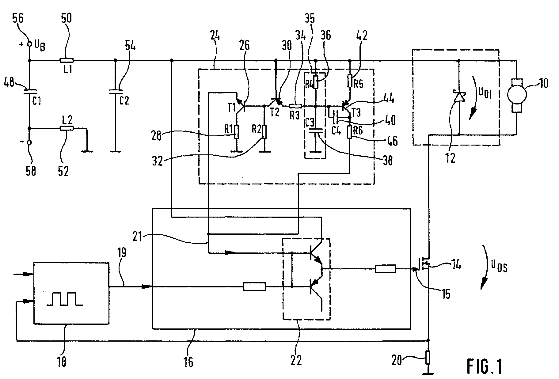
- FIG. 1 shows a circuit arrangement for activation a power output stage
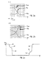
- the figure 2a time-dependent voltage curves the drain voltage of the output stage, the diode voltage on the freewheeling diode and the resulting total voltage during a switch-on process
- the figure 2b corresponding time-dependent voltage curves during switch-off processes
- FIG. 2c shows the time-dependent course the drain voltage with feedback according to the invention.
- An inductive consumer 10 is provided as the electrical load, for example an electric motor.
- This inductive Consumer 10 a free-wheeling diode 12 is connected in parallel.
- the inductive consumer 10 is via a power output stage 14 switched.
- To record the through the power stage 14 flowing current is one against ground interconnected measuring resistor 20 is provided, its potential tapped and fed to a PWM controller 18.
- This A setpoint is also supplied to PWM controller 18.
- the PWM controller 18 Out The setpoint and actual value, the PWM controller 18 generates a control signal 19, which a power stage control 16 as Input variable serves.
- the power stage control 16 comprises a push-pull stage 22 consisting of two transistors, their respective bases are electrically conductive with each other are connected.
- push-pull level 22 The basis of push-pull level 22 are both the control signal 19 via a series resistor and a feedback signal 21 supplied electrically conductive.
- the push-pull level 22 is determined by the positive supply voltage UB fed and on the other hand is connected to ground.
- the emitter of the one transistor of the push-pull stage 22 is over a series resistor with the gate connection of the power output stage 14 connected for forwarding a control signal 15.
- the two transistors of the push-pull stage 22 are as Emitter follower interconnected.
- the supply voltage UB which can be tapped off at the positive pole 56 arrives via a first choke 50 to the parallel connection of the inductive Consumer 10 and the freewheeling diode 12. Between the positive pole 56 and a negative pole 58 is a first capacitance 48 arranged. The minus potential is over a second Throttle 52 led to ground. Furthermore is a second Capacity 54 provided the positive supply potential of inductive consumer 10 couples to ground. First and second inductor 50, 52 and first and second capacitors 48, 54 are used for interference suppression.
- a feedback device 24 is from the positive supply potential controlled as an input variable.
- the positive Supply potential is based on a second Transistor 30 connected, the collector via a second Resistor 32 on the one hand with ground, on the other hand with the Base of a first transistor 26 is connected.
- the collector of the first transistor 26 is through a first resistor 28 switched to ground, the emitter of the first Transistor 26 is the output of a sixth Resistor 46 brought together in an electrically conductive manner and arrives thereafter as a feedback signal 21 to the base of the Push-pull stage 22.
- the feedback device 24 comprises an RC element 35, which consists of a fourth resistor 36 and a third capacitance 38 connected to ground and is fed by the positive supply potential becomes.
- the common potential of the fourth resistor 36 and the third capacitance 38 passes through a third resistor 34 to the emitter of the second transistor 30, on the other hand is the common potential with the base of one third transistor 44 and a fourth capacitance 40 with the collector of the third transistor 44 electrically conductive connected.
- the positive supply potential of the inductive Consumer 10 also passes through the fifth resistor 42 to the emitter of the third transistor 44.
- the Collector output of the third transistor 44 is the sixth resistor 46 with the output potential of the emitter of the first transistor 26 is connected in an electrically conductive manner, so that the feedback signal 21 arises.
- FIG. 1 Circuit The functionality and mode of operation of those shown in FIG. 1 Circuit is now closer with reference to Figures 2a to 2c described.
- the waveforms shown in Figures 2a and 2b show the drain voltage UDS, the diode voltage UDI and the resulting total voltage Uges when switching on ( Figure 2a) and when switching off ( Figure 2b) the power stage 14. If you look at the time-dependent Voltage curve of the total voltage Uges, so one can Detect voltage drop or a voltage peak. This Voltage dips or voltage increases depend on the Switching behavior of the freewheeling diode 12 together. The freewheeling diode 12 must first when switching (switching) occurs clear the junction capacitance to its switching state switch.
- a short circuit occurs for a short time, if the output stage 14 is already controlling the Free-wheeling diode 12, however, is not yet complete Lock mode is located. The result is a dip in voltage the total voltage Uges. This drop in voltage has an effect negative for conducted and radiated interference out. According to the invention, the detected voltage drop is now or voltage increase used to the control signal for the power stage 14 to influence specifically. This influence can be seen in Figure 2c.
- the Power stage 14 controlled with a lower slope, i.e. the switching process is deliberately slowed down. This slowdown in the switching behavior of the power output stage 14 is shown in the second area 62 and - for the Switching off the power stage 14 - as part of the fifth Area 65.
- the power stage control generates 16 a control signal 15 in such a way that the gate voltage UDS of power stage 14 with maximum slope (third area 63) changed until approximately that Ground potential is reached. The same thing happens for the switch-off phase of power stage 14, based on the fourth to sixth regions 64 to 66 are shown.
- the signal curve shown in FIG. 2c can be, for example achieve by the circuit shown in Figure 1.
- the voltage peaks Voltage drop during the switch-on phase, voltage increase during the switch-off phase
- the power stage control 16 in the form of the feedback signal 21. This will only occur in the times until the complete blocking operation or forward operation of the freewheeling diode 12 the switching behavior of the power output stage 14 slows down, causing the resulting EMC interference greatly decrease.
- the power stage control 16 is designed so that the maximum switching speed without feedback the power stage 14 is achieved what in the very steep flanks of the first, third, fourth and sixth areas 61, 63, 64, 66.
- the PWM controller 18 generates a control signal 19 in the Way that the power amplifier 14 are turned on should.
- the power output stage control 16 generates a control signal 15, which has a drain voltage UDS with maximum Switching speed (first area 61) causes. While feedback is not yet active during this period, there is still no feedback signal 21 by the Feedback device generated. Because so far it has exceeded Total voltage Uges not yet the one stored in the RC element 35 Reference voltage, so none of the three transistors 26, 30, 44 controlled.
- the power stage 14 is first with maximum Switching speed controlled. Because of the switching processes a voltage increase occurs in the freewheeling diode 12 the total voltage Uges according to Figure 2b. In the RC link 36 is the voltage level of the total voltage Uges before saved the voltage increase. Exceeds the voltage peak the reference voltage stored in the RC element by a certain amount, the third transistor 44 turned on. Now the positive voltage peak passes the third transistor 44 as a feedback signal 21 to the Basis of the push-pull stage 22. This becomes a control signal 15 generated in such a way that the switching speed reduced.
- the two chokes 50, 52 and the two capacitors 48, 54 are used to improve EMC behavior. Also ensure the two chokes 50, 52 that it is short term actually a detectable voltage drop or to a voltage increase in the total voltage Uges comes. This voltage dip or this voltage increase can be detected more easily and - according to the corresponding Signal adaptation via resistors 25, 32, 34, 42, 46 - also use accordingly as feedback signal 21.
- the circuit described in FIG. 1 can be used analogously can also be used if the power stage 14 at the positive pole and the inductive consumer 10 with free-wheeling diode 12 is connected to the negative pole. The levels are adjust accordingly.
- This circuit is particularly preferred for controlling an adjustment drive in a motor vehicle, for example for fan control or flap adjustment. However, it is not restricted to this.
Landscapes
- Engineering & Computer Science (AREA)
- Power Engineering (AREA)
- Dc-Dc Converters (AREA)
- Control Of Electric Motors In General (AREA)
Abstract
Es wird eine Vorrichtung zur Ansteuerung einer Leistungsendstufe
vorgeschlagen, welche eine Leistungsendstufenansteuerung
(16, 22) umfasst, die in Abhängigkeit von zumindest einem
Steuersignal (19) ein Ansteuersignal (15) erzeugt zur
Ansteuerung zumindest einer Leistungsendstufe (14), welche
eine elektrische Last (10), vorzugsweise eine induktive Last
(10) mit einer Freilaufdiode (12) schaltet, wobei eine Erfassungseinrichtung
(34, 35, 36) vorgesehen ist, die ein Maß
für eine elektrische Größe UGES erfasst, mit der die elektrische
Last (10) beaufschlagt ist. Erfindungsgemäß ist eine
Rückkopplungseinrichtung (24) vorgesehen, die in Abhängigkeit
von dem Maß für die elektrische Größe UGES der Leistungsendstufensansteuerung
(16, 22) zumindest ein Rückkopplungssignal
(21) zuführt zur Beeinflussung des Ansteuersignals
(15).
Description
Die Erfindung geht aus von einer Vorrichtung zur Ansteuerung einer Leistungsendstufe nach der Gattung des unabhängigen Anspruchs. Aus der EP-A 899 860 ist bereits eine Leistungsendstufenschaltung mit PWM-Betrieb und Dauereinschaltbetrieb bekannt. Eine vorgeschaltete Regelschaltung steuert in Abhängigkeit von einem externen vorgebbaren Sollwert, einem Istwert der Leistungsendstufe und einer von der Versorgungsspannung abgeleiteten Bezugsspannung den Pulsweitenmodulationsgenerator und die Leistungsendstufe in einen Dauerausschaltzustand, einen PWM-Betrieb mit pulsweitenmodulierten Pulsen und einen Dauereinschaltzustand. Eine erhöhte Verlustleistung und hohe EMV im Grenzbereich zur Volllast wird dadurch vermieden, dass sie in Abhängigkeit von einem vorgebbaren Sollwert und der Versorgungsspannung vorzeitig vom PWM-Betrieb in den Dauereinschaltbetrieb übergeht und mit einer Hysterese dieser Werte wieder in den PWM-Betrieb zurückkehrt.The invention is based on a control device a power stage according to the genre of the independent Claim. A power output stage circuit is already known from EP-A 899 860 with PWM operation and continuous switch-on operation known. An upstream control circuit controls depending from an external predefinable setpoint, a Actual value of the power output stage and one of the supply voltage derived reference voltage the pulse width modulation generator and the power output stage in a permanent switch-off state, PWM operation with pulse width modulated Pulses and a continuous on state. An increased power loss and high EMC in the limit range to full load thereby avoided that depending on a predefinable Setpoint and the supply voltage prematurely from PWM mode switches to continuous switch-on mode and with a hysteresis of these values returns to PWM operation.
Es ist Aufgabe der vorliegenden Erfindung, eine Leistungsendstufenansteuerung anzugeben, die die EMV-Verträglichkeit weiter erhöht und Verlustleistung reduziert. Diese Aufgabe wird durch die Merkmale des unabhängigen Anspruchs gelöst. The object of the present invention is a power output stage control specify the EMC compatibility further increased and power loss reduced. This task is solved by the features of the independent claim.
Die Erfindung geht aus von einer Vorrichtung zur Ansteuerung einer Leistungsendstufe, die in Abhängigkeit von zumindest einem Steuersignal ein Ansteuersignal für zumindest eine Leistungsendstufe erzeugt, um in einem Schaltbetrieb die Leistungsendstufe anzusteuern, die eine elektrische Last mit induktivem Anteil, vorzugsweise mit einer Freilaufdiode, schaltet. Die Vorrichtung umfasst weiterhin eine Erfassungseinrichtung, die ein Maß für eine elektrische Größe erfasst, mit der die elektrische Last beaufschlagt ist. Sie zeichnet sich dadurch aus, dass eine Rückkopplungseinrichtung vorgesehen ist, die in Abhängigkeit von dem Maß für die elektrische Größe der Leistungsendstufenansteuerung zumindest ein Rückkopplungssignal zuführt zur Beeinflussung des Ansteuersignals. Dadurch können sowohl leitungsgeführte als auch abgestrahlte Störungen insbesondere bei pulsweitenmodulierten Leistungsstellern für induktive Verbraucher in Kraftfahrzeugen weiter reduziert werden, da durch die Rückkopplung eine optimierte Ansteuerung des Leistungshalbleiters ermöglicht wird. Insbesondere durch die Zeitverzögerungen beim Übergang vom leitenden Betrieb auf sperrenden Betrieb oder umgekehrt bei einer einem Elektromotor parallel geschalteten Freilaufdiode werden beim hochfrequenten, steilflankigen Ein- und Ausschalten Störungen verursacht. Diese Zeitverzögerung der Freilaufdiode beim Übergang vom leitenden Betrieb auf sperrenden Betrieb und umgekehrt lässt sich anhand eines Spannungseinbruchs oder einer Spannungserhöhung detektieren und für eine störungsoptimierte Ansteuerung der Leistungsendstufe verwenden. Zu den Zeiten des Übergangs vom leitenden in den nichtleitenden Zustand der Freilaufdiode wird gezielt die Flankensteilheit der Drainspannung der Leistungsendstufe reduziert. Dies wird durch die Rückkopplungseinrichtung erreicht, die ein Rückkopplungssignal an die Leistungsendstufenansteuerung weiterleitet, so dass sich die Schaltgeschwindigkeit der Leistungsendstufe während der Übergangszeit verlangsamt. In Zeiten, in denen der Schaltvorgang der Diode beendet ist, wird die Leistungsendstufe zur Reduzierung der Gesamtverlustleistung mit maximaler Schaltgeschwindigkeit angesteuert, d.h. mit maximaler Flankensteilheit.The invention is based on a control device a power output stage that depends on at least a control signal is a control signal for at least one Power output stage generated to the in a switching operation To control the power output stage with an electrical load inductive component, preferably with a free-wheeling diode, on. The device further comprises a detection device, which measures a measure of an electrical quantity, with which the electrical load is applied. she draws is characterized in that a feedback device is provided which is dependent on the measure of the electrical Size of the power stage control at least one Feedback signal feeds to influence the control signal. This allows both line-guided and radiated Interferences especially with pulse width modulated Power controllers for inductive consumers in motor vehicles can be further reduced since the feedback a optimized control of the power semiconductor enables becomes. Especially due to the time delays during the transition from managerial operation to blocking operation or vice versa with a freewheeling diode connected in parallel with an electric motor are used for high-frequency, steep-sided entry and exit Switching off causes interference. This time delay the Free-wheeling diode during the transition from conductive operation to blocking Operation and vice versa can be based on a voltage dip or detect a voltage increase and for fault-optimized control of the power output stage use. At the time of transition from senior to the non-conductive state of the freewheeling diode is targeted the slope of the drain voltage of the power stage reduced. This is achieved by the feedback device, which a feedback signal to the power stage control forwards so that the switching speed the power stage during the transition period slowed down. At times when the switching process of the Diode is finished, the power output stage for reduction the total power loss at maximum switching speed controlled, i.e. with maximum slope.
In einer zweckmäßigen Weiterbildung ist vorgesehen, dass eine Rückkopplungsaktivierungseinrichtung vorgesehen ist, die die Weiterleitung des Rückkopplungssignals steuert. Die Rückkopplungsaktivierungseinrichtung leitet das Rückkopplungssignal zur Reduzierung der Flankensteilheit nur dann weiter, wenn der Schaltvorgang der Diode noch nicht beendet ist. Dadurch werden Störungen minimiert. Ist jedoch der Schaltvorgang der Diode beendet, so erkennt dies die Rückkopplungsaktivierungseinrichtung anhand des Rückgangs der Spannungserhöhung bzw. Spannungsabsenkung und deaktiviert die Weiterleitung des Rückkopplungssignals. Dadurch kann das Schaltverhalten der Leistungsendstufe gezielt beeinflusst werden, um einerseits während des Schaltvorgangs der Diode die Störungen zu minimieren, andererseits bei Beendigung des Schaltvorgangs der Diode das Schaltverhalten der Leistungsendstufe zu beschleunigen zur Verlustleistungsreduzierung.In an expedient further development it is provided that a Feedback activation device is provided, the controls the forwarding of the feedback signal. The Feedback activation device conducts the feedback signal only to reduce the slope continue if the switching process of the diode has not yet ended is. This minimizes interference. However, it is Switching operation of the diode ended, this recognizes the feedback activation device based on the decline in Voltage increase or decrease and deactivated the forwarding of the feedback signal. This can do that Switching behavior of the power output stage specifically influenced be on the one hand during the switching process of the diode minimize the disturbances, on the other hand when the Switching operation of the diode, the switching behavior of the power output stage to accelerate to reduce power loss.
In einer zweckmäßigen Weiterbildung leitet die Rückkopplungsaktivierungseinrichtung das Rückkopplungssignal dann weiter, wenn das Maß für die elektrische Größe einen Grenzwert über- oder unterschreitet. Denn der Beginn des Schaltvorgangs der Diode macht sich in Form einer Spannungserhöhung bzw. -erniedrigung bemerkbar, die durch Grenzwertvergleich detektiert werden kann.In an expedient development, the feedback activation device guides the feedback signal then continue if the measure of the electrical quantity has a limit exceeds or falls below. Because the beginning of the switching process the diode takes the form of a voltage increase or lowering noticeable by comparison of limits can be detected.
In einer zweckmäßigen Weiterbildung ist vorgesehen, die elektrische Größe in einem Speicherglied, vorzugsweise einem RC-Glied, zwischenzuspeichern als Referenzwert. Übersteigt bzw. unterschreitet die elektrische Grösse den zwischengespeicherten Referenzwert, wird auf einen Spannungspeak geschlossen und die Rückkopplung aktiviert. Als Rückkopplungssignal wird der Spannungspeak verwendet, gegebenenfalls nach Signalanpassungen über Widerstände. Diese analoge Schaltungsrealisierung gewährleistet eine störungs- und verlustminimierte Ansteuerung der Leistungsendstufe.In an expedient further training it is provided that electrical quantity in a memory element, preferably one RC element, to be buffered as a reference value. exceeds or falls below the electrical size of the buffered Reference value, a voltage peak is concluded and activated the feedback. As a feedback signal the voltage peak is used, if necessary after Signal adjustments via resistors. This analog circuit realization ensures a failure and loss minimized Control of the power stage.
Weitere zweckmäßige Weiterbildungen ergeben sich aus weiteren abhängigen Ansprüchen und aus der Beschreibung.Further expedient further developments result from further dependent claims and from the description.
Die Erfindung wird anhand eines in den Zeichnungen dargestellten Ausführungsbeispiels näher erläutert.The invention is illustrated by means of one in the drawings Embodiment explained in more detail.
Es zeigen Figur 1 eine Schaltungsanordnung zur Ansteuerung einer Leistungsendstufe, die Figur 2a zeitabhängige Spannungsverläufe der Drainspannung der Endstufe, der Diodenspannung an der Freilaufdiode sowie die resultierende Gesamtspannung bei einem Einschaltvorgang, die Figur 2b die entsprechenden zeitabhängigen Spannungsverläufe bei Ausschaltvorgängen sowie die Figur 2c den zeitabhängigen Verlauf der Drainspannung bei erfindungsgemäßer Rückkopplung.FIG. 1 shows a circuit arrangement for activation a power output stage, the figure 2a time-dependent voltage curves the drain voltage of the output stage, the diode voltage on the freewheeling diode and the resulting total voltage during a switch-on process, the figure 2b corresponding time-dependent voltage curves during switch-off processes and FIG. 2c shows the time-dependent course the drain voltage with feedback according to the invention.
Als elektrische Last ist ein induktiver Verbraucher 10 vorgesehen,
beispielsweise ein Elektromotor. Diesem induktiven
Verbraucher 10 ist eine Freilaufdiode 12 parallel geschaltet.
Der induktive Verbraucher 10 wird über eine Leistungsendstufe
14 geschaltet. Zur Erfassung des durch die Leistungsendstufe
14 fliessenden Stroms ist ein gegen Masse
verschalteter Messwiderstand 20 vorgesehen, dessen Potential
abgegriffen und einer PWM-Steuerung 18 zugeführt ist. Dieser
PWM-Steuerung 18 ist außerdem ein Sollwert zugeführt. Aus
Soll- und Istwert erzeugt die PWM-Steuerung 18 ein Steuersignal
19, welches einer Leistungsendstufenansteuerung 16 als
Eingangsgröße dient. Die Leistungsendstufenansteuerung 16
umfasst eine Push-Pull-Stufe 22, bestehend aus zwei Transistoren,
deren jeweilige Basis elektrisch leitend miteinander
verbunden sind. Der Basis der Push-Pull-Stufe 22 sind sowohl
das Steuersignal 19 über einen Vorwiderstand sowie ein Rückkopplungssignal
21 elektrisch leitend zugeführt. Die Push-Pull-Stufe
22 wird durch die positive Versorgungsspannung UB
gespeist und ist andererseits mit Masse verbunden. Der Emitter
des einen Transistors der Push-Pull-Stufe 22 ist über
einen Vorwiderstand mit dem Gateanschluss der Leistungsendstufe
14 verbunden zur Weiterleitung eines Ansteuersignals
15. Die beiden Transistoren der Push-Pull-Stufe 22 sind als
Emitterfolger verschaltet.An
Die am Pluspol 56 abgreifbare Versorgungsspannung UB gelangt
über eine erste Drossel 50 an die Parallelschaltung des induktiven
Verbrauchers 10 und der Freilaufdiode 12. Zwischen
dem Pluspol 56 und einem Minuspol 58 ist eine erste Kapazität
48 angeordnet. Das Minuspotential wird über eine zweite
Drossel 52 gegen Masse geführt. Weiterhin ist eine zweite
Kapazität 54 vorgesehen, die das positive Versorgungspotential
des induktiven Verbrauchers 10 gegen Masse koppelt. Erste
und zweite Drossel 50, 52 sowie erste und zweite Kapazität
48, 54 dienen der Entstörung.The supply voltage UB which can be tapped off at the
Eine Rückkopplungseinrichtung 24 wird von dem positiven Versorgungspotential
als Eingangsgröße angesteuert. Das positive
Versorgungspotential ist mit der Basis eines zweiten
Transistors 30 verbunden, dessen Kollektor über einen zweiten
Widerstand 32 einerseits mit Masse, andererseits mit der
Basis eines ersten Transistors 26 verbunden ist. Der Kollektor
des ersten Transistors 26 ist über einen ersten Widerstand
28 gegen Masse geschaltet, der Emitter des ersten
Transistors 26 wird mit dem Ausgangssignal eines sechsten
Widerstands 46 elektrisch leitend zusammengeführt und gelangt
danach als Rückkopplungssignal 21 an die Basis der
Push-Pull-Stufe 22. Die Rückkopplungseinrichtung 24 umfasst
ein RC-Glied 35, welches aus einem vierten Widerstand 36 und
einer dritten Kapazität 38, gegen Masse geschaltet, gebildet
ist und von dem positiven Versorgungspotential gespeist
wird. Das gemeinsame Potential des vierten Widerstands 36
und der dritten Kapazität 38 gelangt über einen dritten Widerstand
34 an den Emitter des zweiten Transistors 30, andererseits
ist das gemeinsame Potential mit der Basis eines
dritten Transistors 44 sowie über eine vierte Kapazität 40
mit dem Kollektor des dritten Transistors 44 elektrisch leitend
verbunden. Das positive Versorgungspotential des induktiven
Verbrauchers 10 gelangt außerdem über den fünften Widerstand
42 an den Emitter des dritten Transistors 44. Der
Kollektorausgang des dritten Transistors 44 wird über den
sechsten Widerstand 46 mit dem Ausgangspotential des Emitters
des ersten Transistors 26 elektrisch leitend verbunden,
so dass das Rückkopplungssignal 21 entsteht.A
Die Funktionalität und Wirkungsweise der in Figur 1 gezeigten
Schaltung wird nun anhand der Figuren 2a bis 2c näher
beschrieben. Die in den Figuren 2a und 2b dargestellten Signalverläufe
zeigen die Drainspannung UDS, die Diodenspannung
UDI sowie die daraus resultierende Gesamtspannung Uges
beim Einschalten (Figur 2a) und beim Ausschalten (Figur 2b)
der Leistungsendstufe 14. Betrachtet man den zeitabhängigen
Spannungsverlauf der Gesamtspannung Uges, so lässt sich ein
Spannungseinbruch bzw. ein Spannungspeak feststellen. Diese
Spannungseinbrüche bzw. Spannungserhöhungen hängen mit dem
Schaltverhalten der Freilaufdiode 12 zusammen. Die Freilaufdiode
12 muss bei den auftretenden (Um-)Schaltvorgängen erst
die Sperrschichtkapazität freiräumen, um ihren Schaltzustand
zu wechseln. Es kommt quasi kurzzeitig zu einem Kurzschluss,
wenn die Leistungsendstufe 14 bereits durchsteuert, die
Freilaufdiode 12 sich jedoch noch nicht in dem vollständigen
Sperrbetrieb befindet. Die Folge ist ein Spannungseinbruch
der Gesamtspannung Uges. Dieser Spannungseinbruch wirkt sich
negativ auf leitungsgebundene und abgestrahlte Störungen
aus. Erfindungsgemäß wird nun die detektierte Spannungsabsenkung
bzw. Spannungserhöhung dazu verwendet, um das Ansteuersignal
für die Leistungsendstufe 14 gezielt zu beeinflussen.
Diese Beeinflussung wird aus Figur 2c ersichtlich.
Während des Umschaltvorgangs der Freilaufdiode 12 wird die
Leistungsendstufe 14 mit einer geringeren Steilheit angesteuert,
d.h. der Schaltvorgang wird bewusst verlangsamt.
Diese Verlangsamung des Schaltverhaltens der Leistungsendstufe
14 zeigt sich im zweiten Bereich 62 sowie - für das
Abschalten der Leistungsendstufe 14 - im Rahmen des fünften
Bereichs 65. Ist der Umschaltvorgang der Freilaufdiode 12
abgeschlossen, was anhand der Beendigung des Spannungseinbruchs
bzw. der Spannungserhöhung der Gesamtspannung Uges
erkannt wird, so erzeugt die Leistungsendstufenansteuerung
16 ein Ansteuersignal 15 in der Weise, dass sich die Gatespannung
UDS der Leistungsendstufe 14 mit maximaler Steilheit
(dritter Bereich 63) verändert, bis näherungsweise das
Massepotential erreicht ist. Entsprechendes geschieht auch
für die Ausschaltphase der Leistungsendstufe 14, anhand der
vierten bis sechsten Bereiche 64 bis 66 gezeigt.The functionality and mode of operation of those shown in FIG. 1
Circuit is now closer with reference to Figures 2a to 2c
described. The waveforms shown in Figures 2a and 2b
show the drain voltage UDS, the diode voltage
UDI and the resulting total voltage Uges
when switching on (Figure 2a) and when switching off (Figure 2b)
the
Der in Figur 2c dargestellte Signalverlauf lässt sich beispielsweise
durch die in Figur 1 gezeigte Schaltung erreichen.
Durch die Rückkopplungseinrichtung 24 werden die Spannungspeaks
(Spannungseinbruch bei der Einschaltphase, Spannungserhöhung
bei der Ausschaltphase), die durch das zeitverzögerte
Schaltverhalten der Freilaufdiode 12 entstehen,
zum Zeitpunkt ihres Entstehens auf die Leistungsendstufenansteuerung
16 in Form des Rückkopplungssignals 21 gegengekoppelt.
Dadurch wird nur in den Zeiten bis zum Erreichen des
vollständigen Sperrbetriebs oder Durchlassbetriebs der Freilaufdiode
12 das Schaltverhalten der Leistungsendstufe 14
verlangsamt, wodurch sich die resultierenden EMV-Störungen
stark vermindern. Die Leistungsendstufenansteuerung 16 ist
so ausgelegt, dass ohne Rückkopplung die maximale Schaltgeschwindigkeit
der Leistungsendstufe 14 erreicht wird, was
sich in den sehr steilen Flanken der ersten, dritten, vierten
und sechsten Bereiche 61, 63, 64, 66 bemerkbar macht.The signal curve shown in FIG. 2c can be, for example
achieve by the circuit shown in Figure 1.
Through the
In dem RC-Glied 35, welches aus dem vierten Widerstand 36
und der dritten Kapazität 38 besteht, ist quasi der Normalpegel
der Gesamtspannung Uges, d.h. wenn kein Spannungseinbruch
bzw. keine Spannungserhöhung erfolgt, gespeichert.
Nun erzeugt die PWM-Steuerung 18 ein Steuersignal 19 in der
Weise, dass die Leistungsendstufe 14 eingeschaltet werden
soll. Die Leistungsendstufenansteuerung 16 erzeugt ein Ansteuersignal
15, das eine Drainspannung UDS mit maximaler
Schaltgeschwindigkeit (erster Bereich 61) hervorruft. Während
dieser Zeitspanne ist die Rückkopplung noch nicht aktiv,
es wird noch kein Rückkopplungssignal 21 durch die
Rückkopplungseinrichtung erzeugt. Denn bislang überstieg die
Gesamtspannung Uges noch nicht die in dem RC-Glied 35 gespeicherte
Referenzspannung, so dass keiner der drei Transistoren
26, 30, 44 durchsteuert.In the
Anschließend tritt wegen des Umschaltens der Freilaufdiode
12 ein Spannungseinbruch der Gesamtspannung Uges beim Einschaltvorgang
der Leistungsendstufe 14 auf. Unterschreitet
der Spannungseinbruch der Gesamtspannung Uges um einen bestimmten
Betrag den in dem RC-Glied 36 gespeicherten Referenzwert,
bewirken die Spannungsverhältnisse ein Aufsteuern
von erstem und zweitem Transistor 26, 30. Der Spannungseinbruch
der Gesamtspannung Uges gelangt über ersten und zweiten
Transistor 26, 30 als Rückkopplungssignal 21 an die Basis
der Push-Pull-Stufe 22. Das ebenfalls der Basis der
Push-Pull-Stufe 22 zugeführte Steuersignal 19 wird entsprechend
des Spannungseinbruchs durch das Rückkopplungssignal
21 reduziert (Gegenkopplung). Dadurch verringert sich die
Schaltgeschwindigkeit der Leistungsendstufe 14. Die Drainspannung
UDS der Leistungsendstufe 14 fällt dadurch in dem
zweiten Bereich 62 flacher ab als in den ersten und dritten
Bereichen 61, 63, in welchen keine Spannungseinbrüche der
Gesamtspannung Uges detektiert wurden.Then occurs because of the switching of the freewheeling diode
12 a voltage drop in the total voltage Uges during the switch-on
In der Zwischenzeit ist die Freilaufdiode 12 vollkommen umgesteuert.
Dies zeigt sich am Rückgang des Spannungseinbruchs.
Die Gesamtspannung Uges erreicht nun näherungsweise
wieder den im RC-Glied 35 zwischengespeicherten Wert. Erster
und zweiter Transistor 26, 30 steuern nun nicht mehr durch,
so dass kein Rückkopplungssignal 21 an die Basis der Push-Pull-Stufe
22 gelangt. Die Leistungsendstufenansteuerung 16
generiert nun ein Ansteuersignal 15 mit maximaler Schaltgeschwindigkeit,
was sich in Form der maximalen Flankensteilheit
in dem dritten Bereich 63 bemerkbar macht.In the meantime, the freewheeling
Von der PWM-Steuerung 18 gelangt nun ein Steuersignal 19 an
die Leistungsendstufenansteuerung 16, das ein Abschalten der
Leistungsendstufe 14 bewirken soll. In dem vierten Bereich
64 wird die Leistungsendstufe 14 zuerst mit maximaler
Schaltgeschwindigkeit angesteuert. Aufgrund der Umschaltvorgänge
in der Freilaufdiode 12 kommt es zu einer Spannungserhöhung
der Gesamtspannung Uges gemäß Figur 2b. In dem RC-Glied
36 ist das Spannungsniveau der Gesamtspannung Uges vor
der Spannungserhöhung abgespeichert. Übersteigt der Spannungspeak
die in dem RC-Glied gespeicherte Referenzspannung
um einen bestimmten Betrag, so wird der dritte Transistor 44
aufgesteuert. Nun gelangt der positive Spannungspeak über
den dritten Transistor 44 als Rückkopplungssignal 21 an die
Basis der Push-Pull-Stufe 22. Dadurch wird ein Ansteuersignal
15 in der Weise erzeugt, dass sich die Schaltgeschwindigkeit
reduziert. Dies geht einher mit einer weniger großen
Spannungsänderung der Drainspannung UDS in dem fünften Bereich
65. Ist der Umschaltvorgang der Freilaufdiode 12 abgeschlossen,
so reduziert sich die Spannungserhöhung der Gesamtspannung
Uges. Unterschreitet die Spannungserhöhung wieder
einen bestimmten Grenzwert, so wird der dritte Transistor
44 nicht mehr aktiviert. Das Rückkopplungssignal 21
gelangt nicht mehr an die Basis der Push-Pull-Stufe 22. Die
Leistungsendstufe 14 wird nun wieder mit maximaler Schaltgeschwindigkeit
angesteuert (sechster Bereich 66).A
Die beiden Drosseln 50, 52 sowie die beiden Kapazitäten 48,
54 dienen der Verbesserung des EMV-Verhaltens. Außerdem gewährleisten
die beiden Drosseln 50, 52, dass es kurzfristig
auch tatsächlich zu einem detektierbaren Spannungseinbruch
bzw. zu einer Spannungserhöhung der Gesamtspannung Uges
kommt. Dieser Spannungseinbruch bzw. diese Spannungserhöhung
lässt sich dadurch leichter detektieren und - nach entsprechender
Signalanpassung über die Widerstände 25, 32, 34, 42,
46 - auch entsprechend als Rückkopplungssignal 21 verwenden.The two chokes 50, 52 and the two
Die vorbeschriebene Schaltung gemäß Figur 1 kann sinngemäß
auch dann zum Einsatz kommen, wenn die Leistungsendstufe 14
an dem Pluspol und der induktive Verbraucher 10 mit Freilaufdiode
12 am Minuspol angeschlossen ist. Die Pegel sind
entsprechend anzupassen.The circuit described in FIG. 1 can be used analogously
can also be used if the
Bevorzugte Verwendung findet diese Schaltung insbesondere zur Ansteuerung eines Verstellantriebs in einem Kraftfahrzeug, beispielsweise zur Gebläseansteuerung bzw. Klappenverstellung. Sie ist jedoch hierauf nicht eingeschränkt.This circuit is particularly preferred for controlling an adjustment drive in a motor vehicle, for example for fan control or flap adjustment. However, it is not restricted to this.
Claims (10)
Applications Claiming Priority (2)
| Application Number | Priority Date | Filing Date | Title |
|---|---|---|---|
| DE10133389A DE10133389A1 (en) | 2001-07-10 | 2001-07-10 | Device for controlling a power output stage |
| DE10133389 | 2001-07-10 |
Publications (2)
| Publication Number | Publication Date |
|---|---|
| EP1276216A2 true EP1276216A2 (en) | 2003-01-15 |
| EP1276216A3 EP1276216A3 (en) | 2006-07-26 |
Family
ID=7691215
Family Applications (1)
| Application Number | Title | Priority Date | Filing Date |
|---|---|---|---|
| EP02013212A Withdrawn EP1276216A3 (en) | 2001-07-10 | 2002-06-15 | Decide for driving a power output stage |
Country Status (3)
| Country | Link |
|---|---|
| US (1) | US6873141B1 (en) |
| EP (1) | EP1276216A3 (en) |
| DE (1) | DE10133389A1 (en) |
Families Citing this family (2)
| Publication number | Priority date | Publication date | Assignee | Title |
|---|---|---|---|---|
| US7276954B2 (en) * | 2002-06-26 | 2007-10-02 | Kabushiki Kaisha Toyota Jidoshokki | Driver for switching device |
| ITMI20081600A1 (en) * | 2008-09-09 | 2010-03-10 | Cross Technology S R L | ACTUATOR-SENSOR SYSTEM |
Family Cites Families (6)
| Publication number | Priority date | Publication date | Assignee | Title |
|---|---|---|---|---|
| US4837495A (en) * | 1987-10-13 | 1989-06-06 | Astec U.S.A. (Hk) Limited | Current mode converter with controlled slope compensation |
| US4959606A (en) * | 1989-01-06 | 1990-09-25 | Uniphase Corporation | Current mode switching regulator with programmed offtime |
| US5197375A (en) * | 1991-08-30 | 1993-03-30 | The Middleby Corporation | Conveyor oven control |
| DE19736338A1 (en) * | 1997-08-21 | 1999-02-25 | Fahrzeugklimaregelung Gmbh | Power stage switch with PWM operation and continuous switch-on operation |
| DE19740697C1 (en) * | 1997-09-16 | 1999-02-11 | Siemens Ag | Power output stage control method for vehicle fuel injection or ignition |
| US6342822B1 (en) * | 2000-11-28 | 2002-01-29 | Fairchild Semiconductor Corporation | Method and apparatus for implementing improved pulse width modulation |
-
2001
- 2001-07-10 DE DE10133389A patent/DE10133389A1/en not_active Ceased
-
2002
- 2002-06-15 EP EP02013212A patent/EP1276216A3/en not_active Withdrawn
- 2002-07-08 US US10/190,781 patent/US6873141B1/en not_active Expired - Fee Related
Also Published As
| Publication number | Publication date |
|---|---|
| EP1276216A3 (en) | 2006-07-26 |
| US6873141B1 (en) | 2005-03-29 |
| DE10133389A1 (en) | 2003-01-23 |
Similar Documents
| Publication | Publication Date | Title |
|---|---|---|
| DE10061563B4 (en) | Method and apparatus for switching on and off of power semiconductors, in particular for a variable-speed operation of an asynchronous machine, operating an ignition circuit for gasoline engines, and switching power supply | |
| DE69728715T2 (en) | driver circuit | |
| EP1602169A2 (en) | Control circuit for a switched mode power supply unit | |
| DE102004018823B3 (en) | Power transistor circuit device with control circuit for power transistor provided with current source device providing current dependent on variation in potential supplied to power transistor | |
| DE102012015787B3 (en) | Gate driver for driving gate of switch, has control input for receiving control signal, where amplified output signal is provided by output for controlling gate of switch, while control device is connected between control input and output | |
| DE102009046255B4 (en) | A driving method for a semiconductor switch and circuit arrangement for driving a gate of a switching transistor | |
| EP1715582B1 (en) | Circuit arrangement for driving an electric power switch at high voltage | |
| WO2006125697A1 (en) | Method for controlling an electric motor fed by a constant voltage supply system | |
| DE102004016927A1 (en) | Method for current and voltage regulation for a switching power supply | |
| DE10252827B3 (en) | Circuit arrangement for fast control, especially of inductive loads | |
| EP2193534A1 (en) | Apparatus and method for supplying power to a voltage- or current-releasing switching device | |
| DE10312221A1 (en) | Voltage regulator with variable output impedance has proportionality factor matched to equivalent serial resistance of output capacitor coupled to output terminal of voltage regulator | |
| EP1728324B1 (en) | Control circuitry for controlling a power electronic circuit and method therefor | |
| EP1658676B1 (en) | Circuit and method for conditioning a supply voltage containing voltage peaks | |
| EP3605832B1 (en) | Adaptive holding current for electrically commutated electric motors | |
| EP1737113A2 (en) | Control circuit for regulating current and voltage of a switch mode power supply | |
| EP2732541B1 (en) | Assembly having a potential-isolated electrical power supply device | |
| EP1276216A2 (en) | Decide for driving a power output stage | |
| EP1880096B1 (en) | Method and device for electrically actuating a valve with a mechanical closing element | |
| EP1703629B1 (en) | Method for digital current control | |
| DE10345235B4 (en) | Power supply circuit and method for powering a load | |
| EP1701434A2 (en) | Control circuit for the switch in a switched-mode power supply | |
| DE4330996A1 (en) | Control device for an electric load, particularly an inductive load | |
| DE19718814C2 (en) | Method and device for power control of electrical consumers connected to an AC supply network | |
| DE102009041451B4 (en) | Control unit for electric and / or pneumatic adjusting drives |
Legal Events
| Date | Code | Title | Description |
|---|---|---|---|
| PUAI | Public reference made under article 153(3) epc to a published international application that has entered the european phase |
Free format text: ORIGINAL CODE: 0009012 |
|
| AK | Designated contracting states |
Kind code of ref document: A2 Designated state(s): AT BE CH CY DE DK ES FI FR GB GR IE IT LI LU MC NL PT SE TR |
|
| AX | Request for extension of the european patent |
Free format text: AL;LT;LV;MK;RO;SI |
|
| PUAL | Search report despatched |
Free format text: ORIGINAL CODE: 0009013 |
|
| AK | Designated contracting states |
Kind code of ref document: A3 Designated state(s): AT BE CH CY DE DK ES FI FR GB GR IE IT LI LU MC NL PT SE TR |
|
| AX | Request for extension of the european patent |
Extension state: AL LT LV MK RO SI |
|
| RIC1 | Information provided on ipc code assigned before grant |
Ipc: H02M 3/156 20060101AFI20060616BHEP |
|
| 17P | Request for examination filed |
Effective date: 20070126 |
|
| 17Q | First examination report despatched |
Effective date: 20070226 |
|
| AKX | Designation fees paid |
Designated state(s): DE ES FR GB IT |
|
| STAA | Information on the status of an ep patent application or granted ep patent |
Free format text: STATUS: THE APPLICATION IS DEEMED TO BE WITHDRAWN |
|
| 18D | Application deemed to be withdrawn |
Effective date: 20160105 |