EP1276170B1 - Antenne multibande - Google Patents
Antenne multibande Download PDFInfo
- Publication number
- EP1276170B1 EP1276170B1 EP01202677A EP01202677A EP1276170B1 EP 1276170 B1 EP1276170 B1 EP 1276170B1 EP 01202677 A EP01202677 A EP 01202677A EP 01202677 A EP01202677 A EP 01202677A EP 1276170 B1 EP1276170 B1 EP 1276170B1
- Authority
- EP
- European Patent Office
- Prior art keywords
- patch
- antenna
- slot
- sides
- feed
- Prior art date
- Legal status (The legal status is an assumption and is not a legal conclusion. Google has not performed a legal analysis and makes no representation as to the accuracy of the status listed.)
- Expired - Lifetime
Links
Images


Classifications
-
- H—ELECTRICITY
- H01—ELECTRIC ELEMENTS
- H01Q—ANTENNAS, i.e. RADIO AERIALS
- H01Q9/00—Electrically-short antennas having dimensions not more than twice the operating wavelength and consisting of conductive active radiating elements
- H01Q9/04—Resonant antennas
- H01Q9/0407—Substantially flat resonant element parallel to ground plane, e.g. patch antenna
- H01Q9/0478—Substantially flat resonant element parallel to ground plane, e.g. patch antenna with means for suppressing spurious modes, e.g. cross polarisation
-
- H—ELECTRICITY
- H01—ELECTRIC ELEMENTS
- H01Q—ANTENNAS, i.e. RADIO AERIALS
- H01Q1/00—Details of, or arrangements associated with, antennas
- H01Q1/36—Structural form of radiating elements, e.g. cone, spiral, umbrella; Particular materials used therewith
-
- H—ELECTRICITY
- H01—ELECTRIC ELEMENTS
- H01Q—ANTENNAS, i.e. RADIO AERIALS
- H01Q1/00—Details of, or arrangements associated with, antennas
- H01Q1/36—Structural form of radiating elements, e.g. cone, spiral, umbrella; Particular materials used therewith
- H01Q1/38—Structural form of radiating elements, e.g. cone, spiral, umbrella; Particular materials used therewith formed by a conductive layer on an insulating support
-
- H—ELECTRICITY
- H01—ELECTRIC ELEMENTS
- H01Q—ANTENNAS, i.e. RADIO AERIALS
- H01Q5/00—Arrangements for simultaneous operation of antennas on two or more different wavebands, e.g. dual-band or multi-band arrangements
- H01Q5/30—Arrangements for providing operation on different wavebands
- H01Q5/307—Individual or coupled radiating elements, each element being fed in an unspecified way
- H01Q5/342—Individual or coupled radiating elements, each element being fed in an unspecified way for different propagation modes
- H01Q5/357—Individual or coupled radiating elements, each element being fed in an unspecified way for different propagation modes using a single feed point
- H01Q5/364—Creating multiple current paths
- H01Q5/371—Branching current paths
-
- H—ELECTRICITY
- H01—ELECTRIC ELEMENTS
- H01Q—ANTENNAS, i.e. RADIO AERIALS
- H01Q9/00—Electrically-short antennas having dimensions not more than twice the operating wavelength and consisting of conductive active radiating elements
- H01Q9/04—Resonant antennas
- H01Q9/0407—Substantially flat resonant element parallel to ground plane, e.g. patch antenna
- H01Q9/0442—Substantially flat resonant element parallel to ground plane, e.g. patch antenna with particular tuning means
Definitions
- the present invention relates to multi-band antennas, and in particular to multi-band planar antennas.
- a multi-band antenna is an antenna capable of operating in more than one frequency band.
- Planar antennas such as microstrip patch antennas
- Planar antennas are an increasingly popular form of antenna.
- Planar antennas are relatively compact in structure, relatively lightweight, relatively simple to manufacture and hence relatively inexpensive.
- planar antennas are suitable for internal use, i.e. they can be incorporated within a telecommunications apparatus, for example a mobile telephone handset. Not only does this improve the aesthetic appeal of the apparatus, but it also protects the antenna making it less susceptible to damage.
- a further advantage of planar antennas is that they may be arranged within, say, a telephone handset in such manner that the radiation emitted during use is primarily directed away from the user of the handset.
- United States Patent US 5,955,995 (Silverstein) discloses a planar antenna that is fed at a corner of the patch thereby causing the antenna to resonate at two adjacent frequencies. None of these antennas achieves resonance in multiple discrete frequency bands. US 5,955,995 discloses the preamble of claim 1.
- a patch antenna comprising a generally rectangular conductive patch defined by first and second pairs of opposing sides; a ground plane; a dielectric substrate between the patch and the ground plane; a feed mechanism for providing electromagnetic signals to a feed point on said conductive patch; and one or more slots formed in the patch, each slot being spaced-apart from the sides of the patch, wherein the feed point is located on, or in-line with, a notional line through a corner and the centre of the conductive patch, a first slot comprises an elongate body portion that is located adjacent and parallel with one of said first sides of the patch, characterised in that the antenna further includes a second slot comprising an elongate body portion that is located adjacent and parallel with the other of said first sides of the patch, said first slot including a respective foot slot portion located adjacent to and parallel with a respective second side of the patch, said second slot including a respective foot slot portion located adjacent to and parallel with the respective second sides of the patch.
- the antenna is able to resonate in a plurality of discrete frequency bands. This means that the antenna is capable of multi-band operation without the need for additional resonating patches, shorting pins, matching circuits or multiple feed points.
- the feed mechanism is arranged to provide a direct feed to the conductive patch.
- the feed mechanism may alternatively feed the patch by indirect coupling.
- the antenna is formed from microstrip.
- At least part of at least one of said slots is positioned in close proximity with an edge of the patch so that said at least one slot part radiates electromagnetic energy in a frequency band other than the natural resonant frequency bands of the patch.
- At least one slot includes a first and a second non-parallel slot portions. More preferably, said first and second slot portions are substantially perpendicular with each other. Further preferably, said at least one slot is substantially I-shaped, or H-shaped.
- the conductive patch is generally rectangular in shape and includes a first and a second slot, one on either side of the feed point, each slot having an elongate body portion with a respective foot portion at, or adjacent, either end of the body portion, the slots being arranged so that the respective elongate body portions are substantially parallely disposed with respect to one pair of opposing edges of the patch and that the respective foot portions are located in close proximity with the other pair of opposing patch edges.
- said one pair of opposing patch edges are the patch edges that radiate electromagnetic energy during resonance in a frequency band in respect of which the conductive patch is designed primarily to resonate.
- said first and second slots are substantially I-shaped and said respective foot portions are arranged to be substantially parallely disposed to said other opposing patch edges.
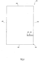
- the handset 10 includes a planar antenna in the preferred form of a microstrip patch antenna 12.
- the patch antenna 12 is mounted on a radio module, or Front End Module (FEM) 14, which in turn is mounted on a printed circuit board (PCB) 16 in conventional manner.
- the antenna 12 comprises a dielectric substrate 20 having a first conductive layer, or patch 18, on one face and a second conductive layer, or ground plane 22, on the opposite face.
- a feed mechanism (not shown in Figure 1) is provided for communication between the FEM 14 and the antenna 12.
- the feed mechanism may be connected directly to the patch (direct feed) or may be coupled indirectly to the patch.
- the FEM 14 sends and receives electromagnetic signals, including radio frequency signals, via the antenna 12 as is conventional.
- the FEM 14 feeds an electrical signal to the antenna 12 via the feed mechanism.
- the signal excites the patch 18 to cause the radiation of electromagnetic energy, or waves, therefrom. More particularly, when the patch 18 is excited by a feed signal, a charge distribution is established on the reverse side, or underside, of the patch 18 and the ground plane. At a particular instant in time, the underside of the patch is positively charged and the ground plane is negatively charged. The attractive forces between these charges tend to hold a large percentage of the charge between the two reverse surfaces.
- a planar, or patch, antenna radiates energy only in frequency bands where resonance occurs.
- the location of the resonant, or operational, frequency band of a patch antenna depends primarily on its dimensions and composition. Thus, when a patch is fed with a signal in the resonant frequency band, the patch radiates energy in that frequency band.
- the efficiency at which the patch radiates energy depends on, amongst other things, whether or not there is an impedance match between the patch 18 and the feed mechanism.
- a coaxial feeder has an impedance of 50 Ohms and it is important therefore to position the feed point such that the effective impedance presented by the patch at the feed point matches the feeder impedance.
- Radiation efficiency may be measured in terms of Return Loss (typically in decibels(dB)) or Voltage Standing Wave Ratio (VSWR).
- RLV Return Loss Value
- a patch antenna 12 is considered as a single band structure with narrow bandwidth i.e. a structure having only one, relatively narrow, resonant frequency band.
- equations [1] to [4] of Figure 7 may be used to determine the approximate required length and width of the patch 18. Normally some fine tuning is then required in order to finalise patch dimensions to suit the application in question.
- the next step in the design of the patch antenna 12 is to determine the position of the point at which the feed mechanism feeds the antenna.
- the feed point is on a notional straight line perpendicular to the patch 18 edges and running through the centre of the patch.
- Such a feed position is hereinafter referred to as a central, or symmetrical, feed position.
- a common way to determine the best position for the feed point is to simulate the operation of the antenna 12 for various feed positions starting on a patch edge moving towards the patch centre along the notional centre line.
- a suitable feed point is found when there is an impedance match between the feed mechanism and the patch (it is noted that in some cases an impedance match is not found on the centre line. In such cases, the normal solution is to enlarge the size of the patch 18 or to provide an impedance matching network between the feed mechanism and the patch 18).
- the current density on the surface of the patch 18 increases significantly along two opposing edges of the patch 18 causing electromagnetic waves to radiate from those edges.
- the current density also increases across the surface of the patch 18 between the two radiating edges and.this causes further electromagnetic radiation from between the two radiating edges.
- the resulting radiation pattern is substantially symmetrical with respect to the patch 18 and this optimises the gain of the antenna. This is the main reason why patch antennas are conventionally fed from a central position.
- a centrally fed patch antenna provides only one resonant frequency band.
- Previous attempts have been made to provide multi-band planar antennas, including multi-band patch antennas. These attempts include stacking or layering two patch antennas one on top of the other, or side-by-side, or using a matching network. Other attempts have involved the combination of slots and shorting pins, or providing multiple feed points. It is considered that such earlier attempts suffer in terms of size and/or complexity. As a result they can be relatively difficult and expensive to manufacture. Moreover, it is considered that the size of such antennas makes them unsuitable for incorporation into modern telecommunication devices, particularly telephone handsets. The problem of size is exacerbated by the fact that many mobile telecommunications networks operate in relatively low frequency bands, low frequency operation normally requiring a large antenna.
- one aspect of the invention provides a single layer planar, or patch, antenna capable of multi-band operation without the use of shorting pins, matching networks or multiple feed points.
- FIGS 2 and 3 illustrate a patch antenna 112, arranged in accordance with a preferred embodiment of the invention, mounted on an FEM 114.
- the antenna 112 comprises a multi-sided patch 118 in the form of a layer of conductive material, particularly conductive metal such as copper or copper alloy.
- the patch 118 coats one face of a substrate 120 made of a dielectric material such as duroid, ceramic or alumina.
- a second conductive layer 122 coats the opposite face of the dielectric substrate 120.
- the second conductive layer. 122 which is typically made from the same material as the patch 118, serves as a ground plane for the antenna 112.
- the antenna 112 includes a feed mechanism 124 for supplying electromagnetic signals (such as radio or microwave signals) in the form of electrical signals between the antenna 112 and the FEM 14.
- the feed mechanism 124 takes the form of a coaxial feeder although a skilled person will appreciate that other forms of conventional feed mechanisin, such as microstrips, striplines and waveguides, may alternatively be used.
- the feeder 124 is preferably arranged to provide a direct feed to the patch 118 and so is fixed to a feed point 126 on the patch 118 itself.
- a non-conductive sleeve 123 formed for example from polytetrafluoroethylene (PTFE), surrounds the body of the feeder 124.
- PTFE polytetrafluoroethylene
- the feed point 126 is positioned on a notional straight line 128 passing through a corner of the patch 118 and the centre of the patch 118.
- the patch is a straight-sided figure, such as the generally rectangular patch 118 shown in the example of Figure 2, the feed point 126 is positioned on, a diagonal of the patch.
- the patch 118 When the feed point 126 is positioned on a diagonal, it is found that the patch 118 resonates in a plurality of different frequency bands. This phenomenon is believed to occur because all sides of the patch are presented to the excitation signal as possible areas from which radiation may emanate. Thus, for the generally rectangular patch 118 of Figure 2, all four sides of the patch 118 are available as possible radiating elements as a result of the diagonally positioned feed point 126. Since the frequency at which radiation occurs depends on patch dimensions, and since the respective opposing sides of the patch 118 are different lengths, the respective resonant states occur in different frequency bands.
- the patch 118 includes two slots 130, 132 for manipulating the performance of the antenna 112 as is described in more detail below.
- Figure 4 shows a plan view of an unslotted patch 218 provided with a diagonally positioned feed point 226.
- the patch 218 dimensions are calculated using equations [1] to [4] of Figure 7 for a desired operational frequency, fr, of approximately 1800 MHz, where the substrate thickness, t, is approximately 1.2 mm and the dielectric constant, ⁇ r, is approximately 10. Accordingly, the length, 1, of the patch 218 is approximately 34.20 mm, and the patch width, w, is approximately 23.37 min.
- the optimal position of the feed point 226 was determined by simulating the operation of the patch 218 with the feed point first positioned at or near a corner 234 of the patch 218 and then subsequently positioned at points progressively nearer the patch centre along the diagonal. For the present design, an impedance match was found when the feed point 226 was positioned 5.70 mm from the longer edge 236 of the patch 218 and 7.98 mm from the shorter edge 238 of the patch 218 as shown in Figure 4. It will be understood that the feed point 226 may equally be positioned along the respective diagonal from any corner of the patch 218.
- Figures 5a to 5c show plots of the current density across the patch 218 at different feed frequencies where resonance occurs.
- Figures 5a to 5c thus show the current density of patch 218 in three different resonant states in three different frequency bands.
- current density is indicated by short dashes on the patch 218 surface, the density of the dashes corresponds to the current density.
- Figure 5a shows the current density when patch 218 is fed with an excitation signal of approximately 1389MHz.
- the main area of high current density is indicated approximately by dashed line 501. This area corresponds to the area of most significant electromagnetic radiation from the patch 218 in this resonant state, the radiation being in a frequency band centred at approximately 1389 MHz.
- a second resonant state occurs when the excitation signal is approximately 1971MHz, and the corresponding current density plot is shown in Figure 5b.
- the main area of high current density is indicated approximately by dashed line 503.
- the key areas of high current density are at and around the mid-sections of the remaining two opposing edges 238, 242 and across the patch 218 between the two edges 238, 242. Consequently, the main radiation of electromagnetic energy in the frequency band around 1971 MHz occurs at and around the mid-sections of the edges 238, 242 and from the patch surface between the edges 238, 242.
- a third resonant state occurs when the excitation signal is approximately 2476 MHz, and the corresponding current density plot is shown in Figure 5c.
- the main area of high current density is indicated approximately by dashed lines 505.
- the key areas of high current density are at and around the mid-sections of all four edges 236, 238, 240, 242. Consequently, the main radiation of electromagnetic energy in the frequency band around 2476 MHz occurs at and around the four edges 236, 238, 240, 242.
- the current density/radiation pattern shown in Figure 5c is dual linear or circularly polarised, meaning that high current density and hence radiation is occurring simultaneously at all four edges in this frequency band.
- the patch 218 is able to radiate energy from all four of its edges 236, 238, 240, 242 in contrast to a conventional centre feed patch which only radiates energy from two opposing edges. This enables the patch 218 to resonate in more than one frequency band.
- Figure 6 shows the Return Loss (dB) for each of the resonant states illustrated in Figures 5a to 5c.
- the first Return Loss Peak 601 represents a resonant, or operational, frequency band centred at approximately 1389 MHz and corresponds with the resonant state shown in Figure 5a.
- the second Return Loss Peak 602 represents a resonant frequency band centred at approximately 1971 MHz and corresponds with the resonant state shown in Figure 5b.
- the third Return Loss Peak 603 represents a resonant frequency band centred at approximately 2476 MHz and corresponds with the resonant state shown in Figure 5c.
- the second Return Loss Peak 602 is significantly better (approximately -13dB) than the first and third Return Loss Peaks 601, 603 (approximately -4dB and -4.5dB respectively). This is expected since the patch 218 was designed particularly for resonance at around 1800 MHz and the feed point 226 was selected to provide a good impedance match in this frequency range. Nonetheless, the first and third Return Loss Peaks 601, 603 are significant and, as is described in more detail below, can be developed to provide additional operating frequency bands for an antenna into which it is incorporated.
- the unslotted patch 218 with diagonal feed may be incorporated into an antenna of the general type illustrated in Figures 2 and 3 and the resulting antenna is capable of operating in a number of different frequency bands. This is achieved using only a single conductive layer for the patch 218, using only a single feed mechanism and without the need for shorting pins or a matching circuit.
- the relatively poor Return Loss Peaks 601, 603 for the first and third frequency bands are normally considered to be unsatisfactory for commercial use.
- the three illustrated Return Loss Peaks 601, 602, 603 are in frequency bands that are not currently in commercial use in the mobile telecommunication industry.
- GSM Global System for Mobile telecommunications - approx. 890 to 960 MHz
- GPS Global Positioning System - approx. 1.57 to 1.58 GHz
- DCS Digital Communication System - approx. 1.71 to 1.88 GHz
- Bluetooth approximately 2.4 to 2.48 GHz
- slots increases the current density in the patch around at least some of the slot edges.
- An increase in current density has the effect of making the patch electrically larger and this makes the patch behave as if it were physically larger even though the actual length and width of the patch are unchanged.
- a slot including slot shape, slot size and slot position
- one or more of the frequency bands in which the patch resonates can be adjusted.
- the frequency band can be lowered (i.e. resonance occurs at a lower frequency). This is because the increase in current density caused by the presence of the slot causes the patch to behave as if it were larger - and larger patches generally resonate at lower frequencies.
- the slots also provide a further effect when arranged in accordance with the invention.
- the increased surface current density around the slot edges gives rise to additional Return Loss Peaks in different frequency bands.
- the slot edges when appropriately placed, act as pseudo patch edges from which electromagnetic energy can radiate.
- a slot can therefore effectively create one or more further resonant states for the patch and so increase the versatility of the antenna.
- the provision of a slot on the patch can also affect the effective impedance of the patch with respect to the feed point. The slot can therefore affect the magnitude of the Return Loss Peak in one or more resonant frequency bands.
- the natural resonance frequency bands of a planar antenna can be adjusted, further resonance frequency bands, i.e. operational frequencies, can be created and the return loss value (i.e. patch efficiency) in resonance frequency bands can be improved.
- the return loss value i.e. patch efficiency
- removal of material from a patch to form a slot can be detrimental to the efficiency of the antenna and this must be taken into account during slot design.
- More than one slot is preferred as it facilitates the adjustment of a larger number of frequency bands - for example, one slot can be used to adjust the frequency value and/or return loss value primarily in one resonant frequency state, while another slot can be used to adjust the frequency value and/or return loss value primarily in another resonant frequency state.
- a slot or part-slot
- moving a slot (or part-slot) into or towards an area of higher.radiation density further increases current density and lowers frequency.
- the slot(s) can give rise to additional resonant states that are not appreciable in an unslotted patch. This is particularly the case when the slot(s) (or part-slot(s)) are located in close proximity with, and substantially in parallel with, a patch edge.
- the resonance states of both a slotted or unslotted patch may occur in different frequency bands to those described above and so the slots may have effect in different frequency bands.
- slot design techniques described herein may be applied to patches that are not necessarily fed from a point on a diagonal.
- Having more than one slot in the patch is preferred as this facilitates manipulation of more than one operational frequency. It will be appreciated, however, that an operable patch may also be achieved using only one slot.
- the or each slot does not necessarily have to be I-shaped. It is preferred, however, that at least one slot includes a first and a second non-parallel slot portions. This increases the length of slot edges in a given area (for example around the feet) which increases the effect that the slot has on the operational frequencies. More preferably, the first and second slot portions are substantially perpendicular with each other. This is particularly useful for generally rectangular patches as it allows the slot to be positioned with a respective portion substantially parallel with a respective patch edge. For a non-rectangular patch, the relative angle between the first and second slot portions can be set accordingly.
- the feet portions of the slot need not necessarily be located at the very end of the body portion.
- the second non-parallel slot portion need not necessarily be integral with the first slot portion.
- the feet portions may be detached from the body portion. This results in a decrease in current density particularly in the area between the feet portions and the body portion. The reduction in current density leads to an increase in operational frequency in the resonant states where the key radiation areas include the area around the feet portions. It is also found that separating the feet from the body improves the return loss value in the DCS frequency band
- the feet portions of an I-shaped slot may be omitted. This leads to a decrease in current density in the areas where the feet would have been which in turn leads to an increase in operational frequency in the resonant states where the key radiation areas include the area around the feet portions
- a further alternative is to omit at least part of the body portion of the slot.
- the mid-portion of the slot body may be removed to leave two spaced apart T-shaped slots. This arrangement is suitable in cases where the patch is intended for operation in frequency bands where the mid-portions of the slots do not play a significant role.
- an antenna it is generally desirable for an antenna to produce as symmetrical a radiation pattern as possible, and so it is preferred if the slots are generally symmetrical in shape and generally symmetrical in arrangement in the patch.
- the invention is not limited to use with antennas in which the patch is fed directly with an excitation signal.
- Other conventional feed arrangements such as coupling, coplanar waveguide or microstrip feedline, can also be used.
- the feed point is arranged, in accordance with the invention, to be on, or in-line with, a notional line from a corner of the patch to the centre of the patch.
- the patch 118, 218 is capable of both transmitting and receiving signals in multiple frequency bands.
- the patch 218, of the invention is mounted on a front end module (FEM) that is arranged for both transmitting and receiving signals in the appropriate frequency bands.
- FEM front end module
- the patch 218, may alternatively be used with an FEM that is receive-only or transmit-only.
- the patches 118, 218, may resonate in further frequency bands than described herein.
- a small Return Loss Peak 604 is present at approximately 2750 MHz.
- additional Return Loss Peaks are not utilised by the preferred embodiment of the invention.
Claims (8)
- Antenne patch (12) comprenant un patch conducteur généralement rectangulaire (118) défini par des première et deuxième paires de côtés opposés ; un plan de masse (122) ; un substrat diélectrique (120) entre le patch et le plan de masse ; un mécanisme d'alimentation (124) pour fournir des signaux électromagnétiques à un point d'alimentation (126, 226) sur ledit patch conducteur ; et une ou plusieurs fentes (130, 132) formées dans le patch, chaque fente étant espacée des côtés du patch, dans laquelle le point d'alimentation (126, 226) est situé ou aligné sur une ligne notionnelle passant par un coin et le centre du patch conducteur, une première fente comprend une partie de corps allongée qui est située à proximité de l'un desdits premiers côtés du patch, et parallèlement à ce côté, caractérisée en ce que l'antenne comporte en outre une deuxième fente (132) comprenant une partie de corps allongée qui est située à proximité de l'autre desdits premiers côtés du patch, et parallèlement à ce côté, ladite première fente (130) comportant une partie de fente de pied respective située à proximité d'un deuxième côté respectif du patch, et parallèlement à ce côté, ladite deuxième fente (132) comportant une partie de fente de pied respective située à proximité des deuxièmes côtés respectifs du patch, et parallèlement à ces côtés.
- Antenne selon la revendication 1, dans laquelle lesdites parties de fente de pied sont formées de façon intégrante avec les parties de corps allongées respectives de la première ou de la deuxième fente respectivement.
- Antenne selon l'une quelconque des revendications précédentes, dans laquelle les côtés de la première paire sont plus courts que les côtés (240, 246) de la deuxième paire.
- Antenne selon l'une quelconque des revendications précédentes, dans laquelle le mécanisme d'alimentation (124) est agencé pour fournir une alimentation directe au patch conducteur.
- Antenne selon l'une quelconque des revendications précédentes, dans laquelle l'antenne est formée à partir d'un microruban.
- Antenne selon l'une quelconque des revendications précédentes, dans laquelle lesdites première et deuxième fentes sont essentiellement en forme de H.
- Antenne selon l'une quelconque des revendications précédentes, dans laquelle lesdites première et deuxième fentes (130, 132) sont situées l'une et l'autre de chaque côté du point d'alimentation (124), chaque fente ayant une partie de corps allongée avec une partie de pied respective située à l'une ou l'autre extrémité, ou à proximité de l'une ou l'autre extrémité, de la partie de corps, les parties de corps allongées respectives étant disposées essentiellement parallèlement relativement à une paire respective de premiers côtés opposés du patch, les parties de pied respectives étant situées à proximité de la deuxième paire de côtés de patch opposés.
- Antenne selon la revendication 1, dans laquelle ladite première paire de côtés de patch opposés sont les côtés de patch qui rayonnent l'énergie électromagnétique durant la résonance dans une bande de fréquences relativement à laquelle le patch conducteur est conçu essentiellement pour résonner.
Priority Applications (3)
| Application Number | Priority Date | Filing Date | Title |
|---|---|---|---|
| EP01202677A EP1276170B1 (fr) | 2001-07-12 | 2001-07-12 | Antenne multibande |
| AT01202677T ATE338354T1 (de) | 2001-07-12 | 2001-07-12 | Mehrbandantenne |
| DE60122698T DE60122698T2 (de) | 2001-07-12 | 2001-07-12 | Mehrbandantenne |
Applications Claiming Priority (1)
| Application Number | Priority Date | Filing Date | Title |
|---|---|---|---|
| EP01202677A EP1276170B1 (fr) | 2001-07-12 | 2001-07-12 | Antenne multibande |
Publications (2)
| Publication Number | Publication Date |
|---|---|
| EP1276170A1 EP1276170A1 (fr) | 2003-01-15 |
| EP1276170B1 true EP1276170B1 (fr) | 2006-08-30 |
Family
ID=8180633
Family Applications (1)
| Application Number | Title | Priority Date | Filing Date |
|---|---|---|---|
| EP01202677A Expired - Lifetime EP1276170B1 (fr) | 2001-07-12 | 2001-07-12 | Antenne multibande |
Country Status (3)
| Country | Link |
|---|---|
| EP (1) | EP1276170B1 (fr) |
| AT (1) | ATE338354T1 (fr) |
| DE (1) | DE60122698T2 (fr) |
Families Citing this family (10)
| Publication number | Priority date | Publication date | Assignee | Title |
|---|---|---|---|---|
| PT103299B (pt) * | 2005-06-29 | 2007-04-30 | Univ Do Minho | Microantena integrada sintonizável com dimensões eléctricas reduzidas e seu método de fabrico |
| GB2453160B (en) * | 2007-09-28 | 2009-09-30 | Motorola Inc | Radio frequency antenna |
| KR101338787B1 (ko) * | 2012-02-09 | 2013-12-06 | 주식회사 에이스테크놀로지 | 레이더 배열 안테나 |
| US9300050B2 (en) | 2013-02-22 | 2016-03-29 | Bang & Olufsen A/S | Multiband RF antenna |
| US9954285B2 (en) * | 2014-09-12 | 2018-04-24 | Taoglas Group Holdings Limited | WiFi patch antenna with dual u-shaped slots |
| DE102016011815B3 (de) * | 2016-10-05 | 2018-02-15 | IAD Gesellschaft für Informatik, Automatisierung und Datenverarbeitung mbH | Betriebsgerät mit gestaffeltem Überspannungs- und Überstromschutz für die Ansteuerung von intelligenten Leuchtmitteln und Geräten sowie Leuchtmittel mit diesem Betriebsgerät |
| EP3343697B1 (fr) | 2016-12-30 | 2020-08-12 | Nxp B.V. | Antenne patch |
| CN112635981B (zh) * | 2019-09-24 | 2023-08-22 | 上海诺基亚贝尔股份有限公司 | 天线组件、天线阵列和通信设备 |
| CN112928480B (zh) * | 2021-02-05 | 2023-03-14 | 东莞泰升音响科技有限公司 | 一种新型ltcc贴片式蓝牙天线 |
| GB2624348A (en) * | 2021-09-23 | 2024-05-15 | Rogers Corp | Dual band antenna |
Family Cites Families (1)
| Publication number | Priority date | Publication date | Assignee | Title |
|---|---|---|---|---|
| US6181281B1 (en) * | 1998-11-25 | 2001-01-30 | Nec Corporation | Single- and dual-mode patch antennas |
-
2001
- 2001-07-12 DE DE60122698T patent/DE60122698T2/de not_active Expired - Lifetime
- 2001-07-12 AT AT01202677T patent/ATE338354T1/de not_active IP Right Cessation
- 2001-07-12 EP EP01202677A patent/EP1276170B1/fr not_active Expired - Lifetime
Also Published As
| Publication number | Publication date |
|---|---|
| EP1276170A1 (fr) | 2003-01-15 |
| DE60122698T2 (de) | 2007-08-30 |
| ATE338354T1 (de) | 2006-09-15 |
| DE60122698D1 (de) | 2006-10-12 |
Similar Documents
| Publication | Publication Date | Title |
|---|---|---|
| US6650294B2 (en) | Compact broadband antenna | |
| KR100307338B1 (ko) | 안테나및안테나용신호방향설정방법 | |
| US6424300B1 (en) | Notch antennas and wireless communicators incorporating same | |
| US6268831B1 (en) | Inverted-f antennas with multiple planar radiating elements and wireless communicators incorporating same | |
| KR100906510B1 (ko) | 안테나 장치 | |
| US7339528B2 (en) | Antenna for mobile communication terminals | |
| US7423591B2 (en) | Antenna system | |
| US6380903B1 (en) | Antenna systems including internal planar inverted-F antennas coupled with retractable antennas and wireless communicators incorporating same | |
| KR100707242B1 (ko) | 유전체 칩 안테나 | |
| US7193576B2 (en) | Ultra wideband bow-tie slot antenna | |
| US20020140607A1 (en) | Internal multi-band antennas for mobile communications | |
| US20050212706A1 (en) | Printed built-in antenna for use in a portable electronic communication apparatus | |
| JP2004088218A (ja) | 平面アンテナ | |
| US20070222699A1 (en) | Embedded antenna | |
| WO2001008260A1 (fr) | Antennes plates a double bande de frequence pour dispositifs de communicaiton sans fil | |
| US20060290575A1 (en) | Antenna integrated into a housing | |
| JP4263972B2 (ja) | 表面実装型アンテナおよびアンテナ装置ならびに無線通信装置 | |
| EP1276170B1 (fr) | Antenne multibande | |
| US20020123312A1 (en) | Antenna systems including internal planar inverted-F Antenna coupled with external radiating element and wireless communicators incorporating same | |
| KR20020065811A (ko) | 전자결합 인쇄 슬롯 마이크로스트립 안테나 | |
| KR100872685B1 (ko) | 역 에프형 안테나 | |
| Wong et al. | Dual‐band plastic chip antenna for GSM/DCS mobile phones | |
| US7149540B2 (en) | Antenna | |
| JP2007503149A (ja) | 高周波およびマイクロ波域用の広帯域アンテナモジュール | |
| EP1560287B1 (fr) | Antenne multifréquence |
Legal Events
| Date | Code | Title | Description |
|---|---|---|---|
| PUAI | Public reference made under article 153(3) epc to a published international application that has entered the european phase |
Free format text: ORIGINAL CODE: 0009012 |
|
| AK | Designated contracting states |
Kind code of ref document: A1 Designated state(s): AT BE CH CY DE DK ES FI FR GB GR IE IT LI LU MC NL PT SE TR |
|
| AX | Request for extension of the european patent |
Free format text: AL;LT;LV;MK;RO;SI |
|
| 17P | Request for examination filed |
Effective date: 20030710 |
|
| AKX | Designation fees paid |
Designated state(s): AT BE CH CY DE DK ES FI FR GB GR IE IT LI LU MC NL PT SE TR |
|
| AXX | Extension fees paid |
Extension state: AL Payment date: 20030715 Extension state: LT Payment date: 20030715 Extension state: RO Payment date: 20030715 Extension state: LV Payment date: 20030715 Extension state: MK Payment date: 20030715 Extension state: SI Payment date: 20030715 |
|
| 17Q | First examination report despatched |
Effective date: 20040205 |
|
| GRAP | Despatch of communication of intention to grant a patent |
Free format text: ORIGINAL CODE: EPIDOSNIGR1 |
|
| GRAS | Grant fee paid |
Free format text: ORIGINAL CODE: EPIDOSNIGR3 |
|
| GRAA | (expected) grant |
Free format text: ORIGINAL CODE: 0009210 |
|
| AK | Designated contracting states |
Kind code of ref document: B1 Designated state(s): AT BE CH CY DE DK ES FI FR GB GR IE IT LI LU MC NL PT SE TR |
|
| AX | Request for extension of the european patent |
Extension state: AL LT LV MK RO SI |
|
| PG25 | Lapsed in a contracting state [announced via postgrant information from national office to epo] |
Ref country code: IT Free format text: LAPSE BECAUSE OF FAILURE TO SUBMIT A TRANSLATION OF THE DESCRIPTION OR TO PAY THE FEE WITHIN THE PRESCRIBED TIME-LIMIT;WARNING: LAPSES OF ITALIAN PATENTS WITH EFFECTIVE DATE BEFORE 2007 MAY HAVE OCCURRED AT ANY TIME BEFORE 2007. THE CORRECT EFFECTIVE DATE MAY BE DIFFERENT FROM THE ONE RECORDED. Effective date: 20060830 Ref country code: FI Free format text: LAPSE BECAUSE OF FAILURE TO SUBMIT A TRANSLATION OF THE DESCRIPTION OR TO PAY THE FEE WITHIN THE PRESCRIBED TIME-LIMIT Effective date: 20060830 Ref country code: AT Free format text: LAPSE BECAUSE OF FAILURE TO SUBMIT A TRANSLATION OF THE DESCRIPTION OR TO PAY THE FEE WITHIN THE PRESCRIBED TIME-LIMIT Effective date: 20060830 Ref country code: NL Free format text: LAPSE BECAUSE OF FAILURE TO SUBMIT A TRANSLATION OF THE DESCRIPTION OR TO PAY THE FEE WITHIN THE PRESCRIBED TIME-LIMIT Effective date: 20060830 Ref country code: BE Free format text: LAPSE BECAUSE OF FAILURE TO SUBMIT A TRANSLATION OF THE DESCRIPTION OR TO PAY THE FEE WITHIN THE PRESCRIBED TIME-LIMIT Effective date: 20060830 Ref country code: CH Free format text: LAPSE BECAUSE OF FAILURE TO SUBMIT A TRANSLATION OF THE DESCRIPTION OR TO PAY THE FEE WITHIN THE PRESCRIBED TIME-LIMIT Effective date: 20060830 Ref country code: LI Free format text: LAPSE BECAUSE OF FAILURE TO SUBMIT A TRANSLATION OF THE DESCRIPTION OR TO PAY THE FEE WITHIN THE PRESCRIBED TIME-LIMIT Effective date: 20060830 |
|
| REG | Reference to a national code |
Ref country code: GB Ref legal event code: FG4D |
|
| REG | Reference to a national code |
Ref country code: CH Ref legal event code: EP |
|
| REG | Reference to a national code |
Ref country code: IE Ref legal event code: FG4D |
|
| REF | Corresponds to: |
Ref document number: 60122698 Country of ref document: DE Date of ref document: 20061012 Kind code of ref document: P |
|
| PG25 | Lapsed in a contracting state [announced via postgrant information from national office to epo] |
Ref country code: DK Free format text: LAPSE BECAUSE OF FAILURE TO SUBMIT A TRANSLATION OF THE DESCRIPTION OR TO PAY THE FEE WITHIN THE PRESCRIBED TIME-LIMIT Effective date: 20061130 Ref country code: SE Free format text: LAPSE BECAUSE OF FAILURE TO SUBMIT A TRANSLATION OF THE DESCRIPTION OR TO PAY THE FEE WITHIN THE PRESCRIBED TIME-LIMIT Effective date: 20061130 |
|
| PG25 | Lapsed in a contracting state [announced via postgrant information from national office to epo] |
Ref country code: ES Free format text: LAPSE BECAUSE OF FAILURE TO SUBMIT A TRANSLATION OF THE DESCRIPTION OR TO PAY THE FEE WITHIN THE PRESCRIBED TIME-LIMIT Effective date: 20061211 |
|
| PG25 | Lapsed in a contracting state [announced via postgrant information from national office to epo] |
Ref country code: PT Free format text: LAPSE BECAUSE OF FAILURE TO SUBMIT A TRANSLATION OF THE DESCRIPTION OR TO PAY THE FEE WITHIN THE PRESCRIBED TIME-LIMIT Effective date: 20070212 |
|
| LTIE | Lt: invalidation of european patent or patent extension |
Effective date: 20060830 |
|
| REG | Reference to a national code |
Ref country code: CH Ref legal event code: PL |
|
| NLV1 | Nl: lapsed or annulled due to failure to fulfill the requirements of art. 29p and 29m of the patents act | ||
| ET | Fr: translation filed | ||
| PLBE | No opposition filed within time limit |
Free format text: ORIGINAL CODE: 0009261 |
|
| STAA | Information on the status of an ep patent application or granted ep patent |
Free format text: STATUS: NO OPPOSITION FILED WITHIN TIME LIMIT |
|
| 26N | No opposition filed |
Effective date: 20070531 |
|
| PG25 | Lapsed in a contracting state [announced via postgrant information from national office to epo] |
Ref country code: GR Free format text: LAPSE BECAUSE OF FAILURE TO SUBMIT A TRANSLATION OF THE DESCRIPTION OR TO PAY THE FEE WITHIN THE PRESCRIBED TIME-LIMIT Effective date: 20061201 Ref country code: MC Free format text: LAPSE BECAUSE OF NON-PAYMENT OF DUE FEES Effective date: 20070731 |
|
| PG25 | Lapsed in a contracting state [announced via postgrant information from national office to epo] |
Ref country code: IE Free format text: LAPSE BECAUSE OF NON-PAYMENT OF DUE FEES Effective date: 20070712 |
|
| PGFP | Annual fee paid to national office [announced via postgrant information from national office to epo] |
Ref country code: FR Payment date: 20080528 Year of fee payment: 8 |
|
| PGFP | Annual fee paid to national office [announced via postgrant information from national office to epo] |
Ref country code: GB Payment date: 20080501 Year of fee payment: 8 |
|
| PGFP | Annual fee paid to national office [announced via postgrant information from national office to epo] |
Ref country code: DE Payment date: 20080809 Year of fee payment: 8 |
|
| PG25 | Lapsed in a contracting state [announced via postgrant information from national office to epo] |
Ref country code: LU Free format text: LAPSE BECAUSE OF NON-PAYMENT OF DUE FEES Effective date: 20070712 Ref country code: CY Free format text: LAPSE BECAUSE OF FAILURE TO SUBMIT A TRANSLATION OF THE DESCRIPTION OR TO PAY THE FEE WITHIN THE PRESCRIBED TIME-LIMIT Effective date: 20060830 |
|
| PG25 | Lapsed in a contracting state [announced via postgrant information from national office to epo] |
Ref country code: TR Free format text: LAPSE BECAUSE OF FAILURE TO SUBMIT A TRANSLATION OF THE DESCRIPTION OR TO PAY THE FEE WITHIN THE PRESCRIBED TIME-LIMIT Effective date: 20060830 |
|
| GBPC | Gb: european patent ceased through non-payment of renewal fee |
Effective date: 20090712 |
|
| REG | Reference to a national code |
Ref country code: FR Ref legal event code: ST Effective date: 20100331 |
|
| PG25 | Lapsed in a contracting state [announced via postgrant information from national office to epo] |
Ref country code: FR Free format text: LAPSE BECAUSE OF NON-PAYMENT OF DUE FEES Effective date: 20090731 |
|
| PG25 | Lapsed in a contracting state [announced via postgrant information from national office to epo] |
Ref country code: GB Free format text: LAPSE BECAUSE OF NON-PAYMENT OF DUE FEES Effective date: 20090712 |
|
| PG25 | Lapsed in a contracting state [announced via postgrant information from national office to epo] |
Ref country code: DE Free format text: LAPSE BECAUSE OF NON-PAYMENT OF DUE FEES Effective date: 20100202 |