EP1272861B1 - A method and test interface for testing digital circuitry - Google Patents
A method and test interface for testing digital circuitry Download PDFInfo
- Publication number
- EP1272861B1 EP1272861B1 EP01933773A EP01933773A EP1272861B1 EP 1272861 B1 EP1272861 B1 EP 1272861B1 EP 01933773 A EP01933773 A EP 01933773A EP 01933773 A EP01933773 A EP 01933773A EP 1272861 B1 EP1272861 B1 EP 1272861B1
- Authority
- EP
- European Patent Office
- Prior art keywords
- buffered
- circuitry
- digital
- signal
- input
- Prior art date
- Legal status (The legal status is an assumption and is not a legal conclusion. Google has not performed a legal analysis and makes no representation as to the accuracy of the status listed.)
- Expired - Lifetime
Links
- 238000012360 testing method Methods 0.000 title claims abstract description 42
- 238000000034 method Methods 0.000 title claims abstract description 9
- 238000006243 chemical reaction Methods 0.000 claims abstract 8
- 230000003139 buffering effect Effects 0.000 claims abstract 6
- 230000000694 effects Effects 0.000 claims description 3
- 230000005540 biological transmission Effects 0.000 description 4
- 238000004519 manufacturing process Methods 0.000 description 3
- 238000013461 design Methods 0.000 description 2
- 230000035945 sensitivity Effects 0.000 description 2
- 230000002457 bidirectional effect Effects 0.000 description 1
- 238000004891 communication Methods 0.000 description 1
- 238000010168 coupling process Methods 0.000 description 1
- 238000005859 coupling reaction Methods 0.000 description 1
- 238000006880 cross-coupling reaction Methods 0.000 description 1
- 230000001419 dependent effect Effects 0.000 description 1
- 238000005516 engineering process Methods 0.000 description 1
- 238000011156 evaluation Methods 0.000 description 1
- 230000003203 everyday effect Effects 0.000 description 1
- 238000009413 insulation Methods 0.000 description 1
- 238000003825 pressing Methods 0.000 description 1
- 238000011084 recovery Methods 0.000 description 1
- 238000001228 spectrum Methods 0.000 description 1
- 238000010998 test method Methods 0.000 description 1
Images


Classifications
-
- G—PHYSICS
- G01—MEASURING; TESTING
- G01R—MEASURING ELECTRIC VARIABLES; MEASURING MAGNETIC VARIABLES
- G01R31/00—Arrangements for testing electric properties; Arrangements for locating electric faults; Arrangements for electrical testing characterised by what is being tested not provided for elsewhere
- G01R31/28—Testing of electronic circuits, e.g. by signal tracer
- G01R31/317—Testing of digital circuits
- G01R31/3181—Functional testing
- G01R31/3185—Reconfiguring for testing, e.g. LSSD, partitioning
-
- G—PHYSICS
- G01—MEASURING; TESTING
- G01R—MEASURING ELECTRIC VARIABLES; MEASURING MAGNETIC VARIABLES
- G01R31/00—Arrangements for testing electric properties; Arrangements for locating electric faults; Arrangements for electrical testing characterised by what is being tested not provided for elsewhere
- G01R31/28—Testing of electronic circuits, e.g. by signal tracer
- G01R31/317—Testing of digital circuits
- G01R31/31712—Input or output aspects
- G01R31/31716—Testing of input or output with loop-back
-
- H—ELECTRICITY
- H04—ELECTRIC COMMUNICATION TECHNIQUE
- H04L—TRANSMISSION OF DIGITAL INFORMATION, e.g. TELEGRAPHIC COMMUNICATION
- H04L1/00—Arrangements for detecting or preventing errors in the information received
- H04L1/24—Testing correct operation
- H04L1/242—Testing correct operation by comparing a transmitted test signal with a locally generated replica
- H04L1/243—Testing correct operation by comparing a transmitted test signal with a locally generated replica at the transmitter, using a loop-back
Definitions
- the invention relates to a method for testing digital circuitry.
- digital full swing high speed data transmission between two integrated circuit chips necessitates the use of a wide-frequency spectrum. Therefore, actual data transmission is very frequency sensitive.
- analog low swing bit stream instead of digital data.
- an analog low swing interface (LSI ) is necessary; note that this abbreviation has a different meaning from everyday usage in electronic technology.
- LSI analog low swing interface
- a standard manufacturing test machine cannot handle the analog input and analog output signals. Therefore, a specific test interface facility should be provided, for executing the actual digital manufacturing tests.
- test facility that in the context of a loop-back configuration will be able to straightforwardly communicate test and/or result patterns to/from the intended destinations and/or sources while minimizing various items thereof with respect to cost, complexity, bandwidth, frequency sensitivity and other parameters that would burden a test manager.
- the invention provides digital circuitry testing as defined by the independent Claims.
- Figure 1 diagrammatically illustrates an archetypical test configuration.
- TESTER block 30 generates and provides test patterns through interconnection facility 32 to the D evice U nder T est 34. After execution of the test, the results of the test through interconnection facility 32 return to the tester block for evaluation, which may result in reject, repair , or pass in whole or in part.
- Tester block 30 may be either a separate device or may be wholly or partially integrated with the device under test. For brevity, external usage of the test results has not been shown in the Figure.
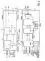
- FIG 2 diagrammatically illustrates a prior art loop-back test system as disclosed more fully in US Patent 5,787,114 , and in particular, Figure 3 thereof.
- parallel digital output patterns 9 are presented to a transmitter 5, serialized by serializer 11, buffered by output buffer 15, clocked by TX clock generators 14, and outputted 6 on a P/N wire pair.
- serial digital input patterns received on a P/N wire pair 7 are buffered by input buffer 16, deserialized by deserializer 12, clock-extracted by Data and Clock Recovery Unit 17 and/or reference-clocked (REFCLK), aligned by Data Alignment Unit 18, and presented as parallel input patterns 4.
- REFCLK reference-clocked
- a switch 19 is closed for effecting loop-back, whereas switch 25 is opened for effecting insulation from the outer world.
- a B uilt- I n- S elf- T est unit 20 may, through generating a wrap-back control 22 and in cooperation with a switch 23 effect a wrapback 10 from the data alignment unit 18 to the serializer 11, thereby effectively limiting the test procedures to only the I/O interface facilities.
- an interconnection 26 with Data Alignment Unit 18 has been shown. For additional detail, reference is had to the full prior art specification.
- FIG. 3 shows the L ow S wing I nterface circuitry to be tested still in normal mode, with a conceptual interface 50 that communicates analog signals between the first comprehensive chip actually shown and a further chip with an appropriate interface not shown.
- the interface to the outer world numbers a Transmit/Receive (RxTx) pair, one for data signals 52 and one for control signals 54.
- RxTx Transmit/Receive
- the core functionality at right in the Circuit comprises by way of example a D igital F unction M aster U nit 62 in which the data handling functionality proper is effected, a S erial I nput/ O utput unit 64, and a D igital Signal P rocessor 66 that is serially and bidirectionally interconnected to SIU 64. Clocking of the latter is effected through gate M3 58 that gets control signals as well as data signals. As shown for brevity, SIU only operates as a data source with respect to the outer world. Furthermore, gate M1 56 presents data to DFMU 62, and synchronizing signals to gate M3 58. Gate M2 57 presents data to the outer world, as received from DFMU 62 and SIU 64. In similar manner, control signals are communicated between LSI 54 and gates M3 58 and M4 60.
- the analog transmitter circuits Tx will convert the digital full swing signal into an analog low swing signal.
- the analog receiver will transform the low swing analog signal back into a full swing digital signal.
- a digital production test machine is not capable to evaluate the analog signals, so that effectively, the instant test interface solves a pressing problem.
- the first one 54 will send the control signals on two paired full-differential lines.
- the second interface 52 effects data transmission on two further likewise paired full-differential lines.
- the Rx of the transmitting LSI is in power-off mode, for data signals just as for control signals. Otherwise, the Tx is switched off while receiving. Therefore, one control signal, not shown for brevity, is needed for every Low Swing Interface circuit.
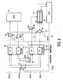
- Figure 4 illustrates the test interface of the present invention operating in actual test mode.
- elements 52, 54, 56, 57, 58, 60, 62, 64, 66 correspond to those of Figure 3 .
- the above two disadvantages are now avoided by this low power for a low swing interface. Such has been effected by the cross-coupling of both interfaces. In consequence, there are now only two conditions for every LSI circuit, as follows:
Landscapes
- Engineering & Computer Science (AREA)
- General Engineering & Computer Science (AREA)
- Physics & Mathematics (AREA)
- General Physics & Mathematics (AREA)
- Computer Networks & Wireless Communication (AREA)
- Signal Processing (AREA)
- Tests Of Electronic Circuits (AREA)
- Input From Keyboards Or The Like (AREA)
- Maintenance And Management Of Digital Transmission (AREA)
Abstract
Description
- The invention relates to a method for testing digital circuitry. In general, digital full swing high speed data transmission between two integrated circuit chips necessitates the use of a wide-frequency spectrum. Therefore, actual data transmission is very frequency sensitive. To reduce frequency sensitivity, it is better to send an analog low swing bit stream instead of digital data. Now, for sending analog bit streams, an analog low swing interface (LSI) is necessary; note that this abbreviation has a different meaning from everyday usage in electronic technology. To ensure correct functionality of this interface it is these low swing interface signals should be rendered digitally testable. However, a standard manufacturing test machine cannot handle the analog input and analog output signals. Therefore, a specific test interface facility should be provided, for executing the actual digital manufacturing tests.
- In consequence, amongst other things, it is an object of the present invention to provide a test facility that in the context of a loop-back configuration will be able to straightforwardly communicate test and/or result patterns to/from the intended destinations and/or sources while minimizing various items thereof with respect to cost, complexity, bandwidth, frequency sensitivity and other parameters that would burden a test manager.
- Now therefore, the invention provides digital circuitry testing as defined by the independent Claims.
- Further advantageous aspects of the invention are recited in dependent Claims.
- These and further aspects and advantages of the invention will be discussed more in detail hereinafter with reference to the disclosure of preferred embodiments, and in particular with reference to the appended Figures that show:
-
Figure 1 , an archetypical test configuration; -
Figure 2 , a prior art loop-back test system; -
Figure 3 , the LSI device in normal mode; -
Figure 4 , the test interface ofFigure 3 's circuitry in actual test mode. -
Figure 1 diagrammatically illustrates an archetypical test configuration. Herein, TESTERblock 30 generates and provides test patterns throughinterconnection facility 32 to the Device UnderT est 34. After execution of the test, the results of the test throughinterconnection facility 32 return to the tester block for evaluation, which may result in reject, repair, or pass in whole or in part.Tester block 30 may be either a separate device or may be wholly or partially integrated with the device under test. For brevity, external usage of the test results has not been shown in the Figure. -
Figure 2 diagrammatically illustrates a prior art loop-back test system as disclosed more fully inUS Patent 5,787,114 , and in particular,Figure 3 thereof. Here, under non-test circumstances, paralleldigital output patterns 9 are presented to atransmitter 5, serialized byserializer 11, buffered byoutput buffer 15, clocked byTX clock generators 14, and outputted 6 on a P/N wire pair. Also, serial digital input patterns received on a P/N wire pair 7 are buffered byinput buffer 16, deserialized bydeserializer 12, clock-extracted by Data andClock Recovery Unit 17 and/or reference-clocked (REFCLK), aligned byData Alignment Unit 18, and presented asparallel input patterns 4. Under test conditions, aswitch 19 is closed for effecting loop-back, whereasswitch 25 is opened for effecting insulation from the outer world. A Built-In-Self-T est unit 20 may, through generating a wrap-back control 22 and in cooperation with aswitch 23 effect awrapback 10 from thedata alignment unit 18 to theserializer 11, thereby effectively limiting the test procedures to only the I/O interface facilities. Furthermore, aninterconnection 26 withData Alignment Unit 18 has been shown. For additional detail, reference is had to the full prior art specification. -
Figure 3 shows the Low Swing Interface circuitry to be tested still in normal mode, with aconceptual interface 50 that communicates analog signals between the first comprehensive chip actually shown and a further chip with an appropriate interface not shown. The interface to the outer world numbers a Transmit/Receive (RxTx) pair, one fordata signals 52 and one forcontrol signals 54. For effecting bidirectional transmission, each time an input lead has been joined to an output lead. No further chip has been shown for brevity. - In contradistinction to the above, the core functionality at right in the Circuit comprises by way of example a Digital
F unction Master Unit 62 in which the data handling functionality proper is effected, a Serial Input/O utput unit 64, and aD igital Signal Processor 66 that is serially and bidirectionally interconnected toSIU 64. Clocking of the latter is effected through gate M3 58 that gets control signals as well as data signals. As shown for brevity, SIU only operates as a data source with respect to the outer world. Furthermore, gate M1 56 presents data to DFMU 62, and synchronizing signals to gate M3 58. Gate M2 57 presents data to the outer world, as received from DFMU 62 and SIU 64. In similar manner, control signals are communicated betweenLSI 54 and gates M3 58 and M4 60. - In this setup, the analog transmitter circuits Tx will convert the digital full swing signal into an analog low swing signal. In its turn, the analog receiver will transform the low swing analog signal back into a full swing digital signal. In fact, a digital production test machine is not capable to evaluate the analog signals, so that effectively, the instant test interface solves a pressing problem.
- In the setup, communication between the two chips necessitates at least two of the interface arrangements. Of these, the first one 54 will send the control signals on two paired full-differential lines. The
second interface 52 effects data transmission on two further likewise paired full-differential lines. To save power and to suppress unwanted self-coupling and instability, the Rx of the transmitting LSI is in power-off mode, for data signals just as for control signals. Otherwise, the Tx is switched off while receiving. Therefore, one control signal, not shown for brevity, is needed for every Low Swing Interface circuit. Now, with this prior art test interface there are three different operating modes: - Transmitting, with Tx on and Rx off.
- Receiving, with Tx off and Rx on.
- Testing, with both Tx and Rx on.
- The providing of these three modes necessitates extra design effort for the power control circuit of the LSI under test, and moreover, for each LSI a second control wire is necessary for effecting these three modes, inasmuch as a single wire is insufficient.
- In this respect,
Figure 4 illustrates the test interface of the present invention operating in actual test mode. Generally,elements Figure 3 . The above two disadvantages are now avoided by this low power for a low swing interface. Such has been effected by the cross-coupling of both interfaces. In consequence, there are now only two conditions for every LSI circuit, as follows: - Transmitting, with Tx on and Rx off.
- Receiving, with Tx off and Rx on.
- Having only these two modes renders it much easier to save power. As shown,
Switches control line 67. Such is also the case for the control LSI and data LSI themselves. The control is provided byblock 66 in the lower right corner of the Figure. Furthermore, the appropriate number of control bits has been indicated with respect to thevarious gates Gate M2 57 needs only one control bit to select between standard data out and test data out.Gate M 1 56 needs two control bits to select between standard data in and test data in, on the one hand, and between various different sources, on the other hand, four possibilities in total in this embodiment as indicated. Likewise,Gate M4 60 needs two control bits to select between standard data out and test data out, on the one hand, and between various different destinations, on the other hand, three possibilities in total in this embodiment as indicated. Likewise,Gate M3 58 needs three control bits to select between standard data in and control in, on the one hand, and between various different sources, on the other hand, four possibilities in total in this embodiment as indicated. - It should be noted that the above-mentioned embodiments illustrate rather than limit the invention, and that those skilled in the art will be able to design many alternative embodiments without departing from the scope of the appended Claims.
Claims (7)
- A method for testing digital circuitry, effecting a paired loop-back (53, 55) from a first buffered output (Tx) to a first buffered input (Rx) whilst within the circuitry executing at least part of the test through using a Built-In-Self-Test methodology,
characterized in that the digital circuitry is arranged to communicate digital signals in an analog form (DATA_P, DATA_N, CON_P, CON_N) with the outside world through a signal conversion interface (52, 54) comprising the first buffered input (Tx) and the first buffered output (Rx), the method being further characterized by effecting said loop-back (53, 55) from at least one of:a first buffered data output to a buffered control input; anda buffered control output to a first buffered data input. - A method as claimed in Claim 1, whilst in connection with said buffering executing a conversion between a digital full swing internal signal and an analog low swing external signal with respect to core circuitry (62) of said digital circuitry.
- A method as claimed in Claim 1, whilst controlling both said loop-back (53, 55) as well as said buffering through a one-bit control signal (67).
- A method as claimed in Claim 3, whilst controlling signal routing between said buffering on the one hand, and test circuitry as well as core circuitry (62) of said digital circuitry, on the other hand, through a plural bit control signal.
- A signal conversion interface (52, 54) for communicating digital signals between digital circuitry and the outside world in an analog form, characterized in that the interface is arranged to effect in an analog form at least one paired loop-back (53, 55) associated with an in-circuit Built-In-Self-Test facility of the digital circuitry from:a first buffered data output (52_Tx) to a buffered control input (54_Rx); anda buffered control output (54_Tx) to a first buffered data input (52_Rx).
- A signal conversion interface (52, 54) as claimed in Claim 5, provided with conversion means for in connection with said buffering executing a conversion between a digital full swing internal signal and an analog low swing external signal with respect to core circuitry (62) said digital circuitry.
- A signal conversion interface (52, 54) as claimed in Claim 5, wherein both said loop-back (53, 55) as well as said buffering have a one-bit control signal input.
Priority Applications (1)
| Application Number | Priority Date | Filing Date | Title |
|---|---|---|---|
| EP01933773A EP1272861B1 (en) | 2000-04-05 | 2001-03-29 | A method and test interface for testing digital circuitry |
Applications Claiming Priority (4)
| Application Number | Priority Date | Filing Date | Title |
|---|---|---|---|
| EP00201242 | 2000-04-05 | ||
| EP00201242 | 2000-04-05 | ||
| PCT/EP2001/003566 WO2001077700A1 (en) | 2000-04-05 | 2001-03-29 | A method and apparatus for testing digital circuitry |
| EP01933773A EP1272861B1 (en) | 2000-04-05 | 2001-03-29 | A method and test interface for testing digital circuitry |
Publications (2)
| Publication Number | Publication Date |
|---|---|
| EP1272861A1 EP1272861A1 (en) | 2003-01-08 |
| EP1272861B1 true EP1272861B1 (en) | 2008-09-10 |
Family
ID=8171311
Family Applications (1)
| Application Number | Title | Priority Date | Filing Date |
|---|---|---|---|
| EP01933773A Expired - Lifetime EP1272861B1 (en) | 2000-04-05 | 2001-03-29 | A method and test interface for testing digital circuitry |
Country Status (6)
| Country | Link |
|---|---|
| US (1) | US6928597B2 (en) |
| EP (1) | EP1272861B1 (en) |
| JP (1) | JP2003530556A (en) |
| AT (1) | ATE408151T1 (en) |
| DE (1) | DE60135735D1 (en) |
| WO (1) | WO2001077700A1 (en) |
Families Citing this family (8)
| Publication number | Priority date | Publication date | Assignee | Title |
|---|---|---|---|---|
| US6656751B2 (en) * | 2001-11-13 | 2003-12-02 | International Business Machines Corporation | Self test method and device for dynamic voltage screen functionality improvement |
| US7111208B2 (en) * | 2002-10-02 | 2006-09-19 | Broadcom Corporation | On-chip standalone self-test system and method |
| US20040193986A1 (en) * | 2003-03-31 | 2004-09-30 | Canagasaby Karthisha S. | On-die pattern generator for high speed serial interconnect built-in self test |
| US7139957B2 (en) * | 2003-06-30 | 2006-11-21 | Intel Corporation | Automatic self test of an integrated circuit component via AC I/O loopback |
| WO2006061668A1 (en) * | 2004-12-07 | 2006-06-15 | Infineon Technologies Ag | Test time reduction for multi-chip modules (mcm) and for system-in-packages (sip) |
| US7855969B2 (en) * | 2005-05-24 | 2010-12-21 | Lsi Corporation | Selective test point for high speed SERDES cores in semiconductor design |
| JP4437986B2 (en) * | 2005-09-30 | 2010-03-24 | 富士通マイクロエレクトロニクス株式会社 | Semiconductor integrated circuit device, interface test control circuit, and test method |
| JP4422134B2 (en) * | 2006-09-29 | 2010-02-24 | Okiセミコンダクタ株式会社 | USB test circuit |
Family Cites Families (5)
| Publication number | Priority date | Publication date | Assignee | Title |
|---|---|---|---|---|
| US5787114A (en) | 1996-01-17 | 1998-07-28 | Lsi Logic Corporation | Loop-back test system and method |
| US5790563A (en) * | 1996-02-05 | 1998-08-04 | Lsi Logic Corp. | Self test of core with unpredictable latency |
| DE19832307C2 (en) * | 1998-07-17 | 2000-09-21 | Siemens Ag | Integrated circuit with a self-test facility |
| US6493124B1 (en) * | 1999-07-27 | 2002-12-10 | Tellabs Operations, Inc. | Looping back signals in optical switches |
| US6348811B1 (en) * | 2000-06-28 | 2002-02-19 | Intel Corporation | Apparatus and methods for testing simultaneous bi-directional I/O circuits |
-
2001
- 2001-03-29 JP JP2001574502A patent/JP2003530556A/en not_active Withdrawn
- 2001-03-29 EP EP01933773A patent/EP1272861B1/en not_active Expired - Lifetime
- 2001-03-29 WO PCT/EP2001/003566 patent/WO2001077700A1/en not_active Ceased
- 2001-03-29 AT AT01933773T patent/ATE408151T1/en not_active IP Right Cessation
- 2001-03-29 DE DE60135735T patent/DE60135735D1/en not_active Expired - Lifetime
- 2001-04-03 US US09/825,279 patent/US6928597B2/en not_active Expired - Lifetime
Also Published As
| Publication number | Publication date |
|---|---|
| US6928597B2 (en) | 2005-08-09 |
| JP2003530556A (en) | 2003-10-14 |
| ATE408151T1 (en) | 2008-09-15 |
| DE60135735D1 (en) | 2008-10-23 |
| US20020053056A1 (en) | 2002-05-02 |
| EP1272861A1 (en) | 2003-01-08 |
| WO2001077700A1 (en) | 2001-10-18 |
Similar Documents
| Publication | Publication Date | Title |
|---|---|---|
| US5956370A (en) | Wrap-back test system and method | |
| US6904375B1 (en) | Method and circuits for testing high speed devices using low speed ATE testers | |
| US5787114A (en) | Loop-back test system and method | |
| US9739834B1 (en) | System and method for transferring serialized test result data from a system on a chip | |
| US6977960B2 (en) | Self test circuit for evaluating a high-speed serial interface | |
| US6397042B1 (en) | Self test of an electronic device | |
| US6807644B2 (en) | JTAG testing arrangement | |
| US7007212B2 (en) | Transmission device, reception device, test circuit, and test method | |
| US7058535B2 (en) | Test system for integrated circuits with serdes ports | |
| CN101485146A (en) | Loopback module based on high-speed serial crossbar switch | |
| KR20040071152A (en) | Testing method and tester for semiconductor integrated circuit device comprising high-speed input/output element | |
| US8135872B2 (en) | USB controller and a testing method of the USB controller | |
| US6631486B1 (en) | Semiconductor integrated circuit and method for testing the same | |
| US6892337B1 (en) | Circuit and method for testing physical layer functions of a communication network | |
| US7496812B1 (en) | Apparatus and method for testing and debugging an integrated circuit | |
| US6928597B2 (en) | Method and apparatus for testing digital circuitry | |
| US9568546B2 (en) | Delay fault testing for chip I/O | |
| US7216269B2 (en) | Signal transmit-receive device, circuit, and loopback test method | |
| EP1573345B1 (en) | Jtag testing arrangement | |
| US7855969B2 (en) | Selective test point for high speed SERDES cores in semiconductor design | |
| JP2000171524A (en) | Semiconductor integrated circuit and inspection method thereof | |
| US6496544B1 (en) | Digital computing system having adaptive communication components | |
| JPH04318732A (en) | Line interface device | |
| JP2002064588A (en) | Digital transmission equipment with built-in pattern generator |
Legal Events
| Date | Code | Title | Description |
|---|---|---|---|
| PUAI | Public reference made under article 153(3) epc to a published international application that has entered the european phase |
Free format text: ORIGINAL CODE: 0009012 |
|
| 17P | Request for examination filed |
Effective date: 20021105 |
|
| AK | Designated contracting states |
Kind code of ref document: A1 Designated state(s): AT BE CH CY DE DK ES FI FR GB GR IE IT LI LU MC NL PT SE TR |
|
| 17Q | First examination report despatched |
Effective date: 20060905 |
|
| 17Q | First examination report despatched |
Effective date: 20060905 |
|
| RAP1 | Party data changed (applicant data changed or rights of an application transferred) |
Owner name: NXP B.V. |
|
| GRAP | Despatch of communication of intention to grant a patent |
Free format text: ORIGINAL CODE: EPIDOSNIGR1 |
|
| RTI1 | Title (correction) |
Free format text: A METHOD AND TEST INTERFACE FOR TESTING DIGITAL CIRCUITRY |
|
| GRAS | Grant fee paid |
Free format text: ORIGINAL CODE: EPIDOSNIGR3 |
|
| GRAA | (expected) grant |
Free format text: ORIGINAL CODE: 0009210 |
|
| AK | Designated contracting states |
Kind code of ref document: B1 Designated state(s): AT BE CH CY DE DK ES FI FR GB GR IE IT LI LU MC NL PT SE TR |
|
| REG | Reference to a national code |
Ref country code: GB Ref legal event code: FG4D |
|
| REG | Reference to a national code |
Ref country code: CH Ref legal event code: EP |
|
| REG | Reference to a national code |
Ref country code: IE Ref legal event code: FG4D |
|
| REF | Corresponds to: |
Ref document number: 60135735 Country of ref document: DE Date of ref document: 20081023 Kind code of ref document: P |
|
| PG25 | Lapsed in a contracting state [announced via postgrant information from national office to epo] |
Ref country code: FI Free format text: LAPSE BECAUSE OF FAILURE TO SUBMIT A TRANSLATION OF THE DESCRIPTION OR TO PAY THE FEE WITHIN THE PRESCRIBED TIME-LIMIT Effective date: 20080910 Ref country code: AT Free format text: LAPSE BECAUSE OF FAILURE TO SUBMIT A TRANSLATION OF THE DESCRIPTION OR TO PAY THE FEE WITHIN THE PRESCRIBED TIME-LIMIT Effective date: 20080910 |
|
| NLV1 | Nl: lapsed or annulled due to failure to fulfill the requirements of art. 29p and 29m of the patents act | ||
| PG25 | Lapsed in a contracting state [announced via postgrant information from national office to epo] |
Ref country code: BE Free format text: LAPSE BECAUSE OF FAILURE TO SUBMIT A TRANSLATION OF THE DESCRIPTION OR TO PAY THE FEE WITHIN THE PRESCRIBED TIME-LIMIT Effective date: 20080910 |
|
| PG25 | Lapsed in a contracting state [announced via postgrant information from national office to epo] |
Ref country code: ES Free format text: LAPSE BECAUSE OF FAILURE TO SUBMIT A TRANSLATION OF THE DESCRIPTION OR TO PAY THE FEE WITHIN THE PRESCRIBED TIME-LIMIT Effective date: 20081221 |
|
| PG25 | Lapsed in a contracting state [announced via postgrant information from national office to epo] |
Ref country code: NL Free format text: LAPSE BECAUSE OF FAILURE TO SUBMIT A TRANSLATION OF THE DESCRIPTION OR TO PAY THE FEE WITHIN THE PRESCRIBED TIME-LIMIT Effective date: 20080910 Ref country code: PT Free format text: LAPSE BECAUSE OF FAILURE TO SUBMIT A TRANSLATION OF THE DESCRIPTION OR TO PAY THE FEE WITHIN THE PRESCRIBED TIME-LIMIT Effective date: 20090210 |
|
| PLBE | No opposition filed within time limit |
Free format text: ORIGINAL CODE: 0009261 |
|
| STAA | Information on the status of an ep patent application or granted ep patent |
Free format text: STATUS: NO OPPOSITION FILED WITHIN TIME LIMIT |
|
| PG25 | Lapsed in a contracting state [announced via postgrant information from national office to epo] |
Ref country code: DK Free format text: LAPSE BECAUSE OF FAILURE TO SUBMIT A TRANSLATION OF THE DESCRIPTION OR TO PAY THE FEE WITHIN THE PRESCRIBED TIME-LIMIT Effective date: 20080910 |
|
| 26N | No opposition filed |
Effective date: 20090611 |
|
| PG25 | Lapsed in a contracting state [announced via postgrant information from national office to epo] |
Ref country code: IT Free format text: LAPSE BECAUSE OF FAILURE TO SUBMIT A TRANSLATION OF THE DESCRIPTION OR TO PAY THE FEE WITHIN THE PRESCRIBED TIME-LIMIT Effective date: 20080910 |
|
| PG25 | Lapsed in a contracting state [announced via postgrant information from national office to epo] |
Ref country code: MC Free format text: LAPSE BECAUSE OF NON-PAYMENT OF DUE FEES Effective date: 20090331 |
|
| REG | Reference to a national code |
Ref country code: CH Ref legal event code: PL |
|
| REG | Reference to a national code |
Ref country code: IE Ref legal event code: MM4A |
|
| PG25 | Lapsed in a contracting state [announced via postgrant information from national office to epo] |
Ref country code: SE Free format text: LAPSE BECAUSE OF FAILURE TO SUBMIT A TRANSLATION OF THE DESCRIPTION OR TO PAY THE FEE WITHIN THE PRESCRIBED TIME-LIMIT Effective date: 20081210 Ref country code: CH Free format text: LAPSE BECAUSE OF NON-PAYMENT OF DUE FEES Effective date: 20090331 Ref country code: IE Free format text: LAPSE BECAUSE OF NON-PAYMENT OF DUE FEES Effective date: 20090329 Ref country code: LI Free format text: LAPSE BECAUSE OF NON-PAYMENT OF DUE FEES Effective date: 20090331 |
|
| PG25 | Lapsed in a contracting state [announced via postgrant information from national office to epo] |
Ref country code: GR Free format text: LAPSE BECAUSE OF FAILURE TO SUBMIT A TRANSLATION OF THE DESCRIPTION OR TO PAY THE FEE WITHIN THE PRESCRIBED TIME-LIMIT Effective date: 20081211 |
|
| PG25 | Lapsed in a contracting state [announced via postgrant information from national office to epo] |
Ref country code: LU Free format text: LAPSE BECAUSE OF NON-PAYMENT OF DUE FEES Effective date: 20090329 |
|
| PG25 | Lapsed in a contracting state [announced via postgrant information from national office to epo] |
Ref country code: TR Free format text: LAPSE BECAUSE OF FAILURE TO SUBMIT A TRANSLATION OF THE DESCRIPTION OR TO PAY THE FEE WITHIN THE PRESCRIBED TIME-LIMIT Effective date: 20080910 |
|
| PG25 | Lapsed in a contracting state [announced via postgrant information from national office to epo] |
Ref country code: CY Free format text: LAPSE BECAUSE OF FAILURE TO SUBMIT A TRANSLATION OF THE DESCRIPTION OR TO PAY THE FEE WITHIN THE PRESCRIBED TIME-LIMIT Effective date: 20080910 |
|
| PGFP | Annual fee paid to national office [announced via postgrant information from national office to epo] |
Ref country code: FR Payment date: 20120410 Year of fee payment: 12 |
|
| PGFP | Annual fee paid to national office [announced via postgrant information from national office to epo] |
Ref country code: GB Payment date: 20120224 Year of fee payment: 12 |
|
| GBPC | Gb: european patent ceased through non-payment of renewal fee |
Effective date: 20130329 |
|
| REG | Reference to a national code |
Ref country code: FR Ref legal event code: ST Effective date: 20131129 |
|
| PG25 | Lapsed in a contracting state [announced via postgrant information from national office to epo] |
Ref country code: GB Free format text: LAPSE BECAUSE OF NON-PAYMENT OF DUE FEES Effective date: 20130329 Ref country code: FR Free format text: LAPSE BECAUSE OF NON-PAYMENT OF DUE FEES Effective date: 20130402 |
|
| REG | Reference to a national code |
Ref country code: DE Ref legal event code: R082 Ref document number: 60135735 Country of ref document: DE Representative=s name: MUELLER-BORE & PARTNER PATENTANWAELTE PARTG MB, DE Ref country code: DE Ref legal event code: R081 Ref document number: 60135735 Country of ref document: DE Owner name: LLL HOLDINGS 6, LLC, WILMINGTON, US Free format text: FORMER OWNER: NXP B.V., EINDHOVEN, NL Ref country code: DE Ref legal event code: R081 Ref document number: 60135735 Country of ref document: DE Owner name: III HOLDINGS 6, LLC, WILMINGTON, US Free format text: FORMER OWNER: NXP B.V., EINDHOVEN, NL |
|
| REG | Reference to a national code |
Ref country code: DE Ref legal event code: R082 Ref document number: 60135735 Country of ref document: DE Representative=s name: MUELLER-BORE & PARTNER PATENTANWAELTE PARTG MB, DE Ref country code: DE Ref legal event code: R081 Ref document number: 60135735 Country of ref document: DE Owner name: III HOLDINGS 6, LLC, WILMINGTON, US Free format text: FORMER OWNER: LLL HOLDINGS 6, LLC, WILMINGTON, DEL., US |
|
| PGFP | Annual fee paid to national office [announced via postgrant information from national office to epo] |
Ref country code: DE Payment date: 20200528 Year of fee payment: 20 |
|
| REG | Reference to a national code |
Ref country code: DE Ref legal event code: R071 Ref document number: 60135735 Country of ref document: DE |