EP1272018A2 - Method of mounting electronic parts with Sn-Zn solder free of Pb - Google Patents
Method of mounting electronic parts with Sn-Zn solder free of Pb Download PDFInfo
- Publication number
- EP1272018A2 EP1272018A2 EP02011952A EP02011952A EP1272018A2 EP 1272018 A2 EP1272018 A2 EP 1272018A2 EP 02011952 A EP02011952 A EP 02011952A EP 02011952 A EP02011952 A EP 02011952A EP 1272018 A2 EP1272018 A2 EP 1272018A2
- Authority
- EP
- European Patent Office
- Prior art keywords
- solder
- electronic parts
- plated layer
- copper foil
- circuit board
- Prior art date
- Legal status (The legal status is an assumption and is not a legal conclusion. Google has not performed a legal analysis and makes no representation as to the accuracy of the status listed.)
- Withdrawn
Links
Images


Classifications
-
- H—ELECTRICITY
- H05—ELECTRIC TECHNIQUES NOT OTHERWISE PROVIDED FOR
- H05K—PRINTED CIRCUITS; CASINGS OR CONSTRUCTIONAL DETAILS OF ELECTRIC APPARATUS; MANUFACTURE OF ASSEMBLAGES OF ELECTRICAL COMPONENTS
- H05K3/00—Apparatus or processes for manufacturing printed circuits
- H05K3/30—Assembling printed circuits with electric components, e.g. with resistors
- H05K3/32—Assembling printed circuits with electric components, e.g. with resistors electrically connecting electric components or wires to printed circuits
-
- H—ELECTRICITY
- H05—ELECTRIC TECHNIQUES NOT OTHERWISE PROVIDED FOR
- H05K—PRINTED CIRCUITS; CASINGS OR CONSTRUCTIONAL DETAILS OF ELECTRIC APPARATUS; MANUFACTURE OF ASSEMBLAGES OF ELECTRICAL COMPONENTS
- H05K3/00—Apparatus or processes for manufacturing printed circuits
- H05K3/22—Secondary treatment of printed circuits
- H05K3/24—Reinforcing of the conductive pattern
- H05K3/244—Finish plating of conductors, especially of copper conductors, e.g. for pads or lands
-
- B—PERFORMING OPERATIONS; TRANSPORTING
- B23—MACHINE TOOLS; METAL-WORKING NOT OTHERWISE PROVIDED FOR
- B23K—SOLDERING OR UNSOLDERING; WELDING; CLADDING OR PLATING BY SOLDERING OR WELDING; CUTTING BY APPLYING HEAT LOCALLY, e.g. FLAME CUTTING; WORKING BY LASER BEAM
- B23K35/00—Rods, electrodes, materials, or media, for use in soldering, welding, or cutting
- B23K35/001—Interlayers, transition pieces for metallurgical bonding of workpieces
- B23K35/007—Interlayers, transition pieces for metallurgical bonding of workpieces at least one of the workpieces being of copper or another noble metal
-
- H—ELECTRICITY
- H05—ELECTRIC TECHNIQUES NOT OTHERWISE PROVIDED FOR
- H05K—PRINTED CIRCUITS; CASINGS OR CONSTRUCTIONAL DETAILS OF ELECTRIC APPARATUS; MANUFACTURE OF ASSEMBLAGES OF ELECTRICAL COMPONENTS
- H05K3/00—Apparatus or processes for manufacturing printed circuits
- H05K3/30—Assembling printed circuits with electric components, e.g. with resistors
- H05K3/32—Assembling printed circuits with electric components, e.g. with resistors electrically connecting electric components or wires to printed circuits
- H05K3/34—Assembling printed circuits with electric components, e.g. with resistors electrically connecting electric components or wires to printed circuits by soldering
- H05K3/346—Solder materials or compositions specially adapted therefor
-
- H—ELECTRICITY
- H10—SEMICONDUCTOR DEVICES; ELECTRIC SOLID-STATE DEVICES NOT OTHERWISE PROVIDED FOR
- H10W—GENERIC PACKAGES, INTERCONNECTIONS, CONNECTORS OR OTHER CONSTRUCTIONAL DETAILS OF DEVICES COVERED BY CLASS H10
- H10W70/00—Package substrates; Interposers; Redistribution layers [RDL]
- H10W70/60—Insulating or insulated package substrates; Interposers; Redistribution layers
- H10W70/67—Insulating or insulated package substrates; Interposers; Redistribution layers characterised by their insulating layers or insulating parts
- H10W70/69—Insulating materials thereof
-
- B—PERFORMING OPERATIONS; TRANSPORTING
- B23—MACHINE TOOLS; METAL-WORKING NOT OTHERWISE PROVIDED FOR
- B23K—SOLDERING OR UNSOLDERING; WELDING; CLADDING OR PLATING BY SOLDERING OR WELDING; CUTTING BY APPLYING HEAT LOCALLY, e.g. FLAME CUTTING; WORKING BY LASER BEAM
- B23K35/00—Rods, electrodes, materials, or media, for use in soldering, welding, or cutting
- B23K35/22—Rods, electrodes, materials, or media, for use in soldering, welding, or cutting characterised by the composition or nature of the material
- B23K35/24—Selection of soldering or welding materials proper
- B23K35/26—Selection of soldering or welding materials proper with the principal constituent melting at less than 400°C
- B23K35/262—Sn as the principal constituent
Definitions
- the present invention relates to a method of mounting various electronic parts on a printed circuit board by soldering.
- PCB printed circuit board
- step 101 a solder paste is printed on lands on a surface of a PCB using a metal mask having holes which are defined complementarily to the lands.
- step 102 surface-mount components including chip parts, QFPs (Quad Flat Packages), SOPs (Small Outline Packages), etc. are placed on the printed solder paste.
- step 103 the PCB with the surface-mount components placed thereon is passed through a high-temperature reflow furnace to melt the solder paste, thus soldering the electrodes of the surface-mount components to the copper foil on the PCB.
- the PCB is inverted in step 104, facing the other surface of the PCB upwardly.
- steps 105, 106 a solder paste is applied to and surface-mount components are placed on the other surface of the PCB in the same manner as with steps 101, 102. Thereafter, components having leads are inserted into through holes in the PCB in step 107. The PCB is then passed through the reflow furnace to melt the solder paste, thus soldering the electrodes of the surface-mount components to the copper foil on the PCB in step 108 in the same manner as with step 103.
- any components which cannot withstand the high temperature in the reflow furnace are manually soldered to the PCB in step 109, thus completing the mounting of necessary electronic parts on the PCB.
- Sn - Ag solder has widely been known as Pb-free solder. Since the properties of Ag are stable, the Sn-Ag solder is as reliable as the Sn - Pb solder when used to mount electronic parts on PCBs.
- One problem of the Sn - Ag solder is that the melting point of the Sn - Ag solder is about 220°C that is higher than the melting point of the Sn - Pb solder which is about 183°C. Therefore, it is difficult to directly use surface-mounting facilities and processes that have used the Sn - Pb solder to solder electronic parts with the Sn - Ag solder.
- Sn - Zn solder Another type of Pb-free solder is Sn - Zn solder. Since the Sn - Zn solder has a melting point of about 197°C, the conventional surface-mounting facilities and electronic parts can directly be used if the Sn - Zn solder is applied to solder the electronic parts.
- the Sn - Zn solder is disadvantageous as compared with the Sn - Pb solder in that Zn is easily oxidizable and makes wetting poor. If electronic parts are mounted on PCBs with the Sn - Zn solder using the conventional surface-mounting facilities and processes, the Sn - Zn solder is not as reliable as the Sn - Pb solder.
- Fig. 3 of the accompanying drawings shows in cross section a prefluxed PCB.
- the PCB has base 10, copper foil 3 disposed on a surface thereof, and flux layer 4 deposited on copper foil 3.
- An interconnection pattern on the PCB is covered with an insulating resist layer, and lands are provided by removing the resist layer from portions of the interconnection pattern.
- the resist layer is omitted from illustration in Fig. 3 and other figures.
- the prefluxing process is widely used in the art as it can reduce the cost of PCBs.
- Electronic parts can be mounted highly reliably on refluxed PCBs using the Sb - Pb solder. If electronic parts are soldered to a PCB with the surface of copper foil being prefluxed, using the Sn - Zn solder, then the Cu of the copper oil and the Zn of the Sn - Zn solder react with each other, forming a Cu - Zn reaction layer in the soldered joints.
- the Cu - Zn reaction layer tends to reduce the bonding strength because it becomes brittle at a high temperature of about 150°C.
- a method of mounting electronic parts on a printed circuit board with Pb-free solder in accordance with the present invention uses a printed circuit board whose surface is treated with Ni/Au, having an interconnection pattern of copper foil, a plated layer of Ni disposed on a surface of the copper foil, and a plated layer of Au disposed on a surface of the plated layer of Ni.
- plated layer of Ni on the surface of copper foil serves as a barrier layer to prevent a Cu - Zn reaction layer, which would otherwise tend to reduce the bonding strength, from being produced in the soldered joints. Therefore, the bonding strength is not lowered when electronic parts are mounted on the printed circuit board using the Sn - Zn solder.
- a printed circuit board (PCB) whose surface is treated with Ni/Au is used as a printed circuit board for mounting electronic parts thereon.
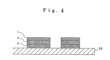
- Fig. 4 shows in cross section a PCB whose surface is treated with Ni/Au, which is used in the method of mounting electronic parts according to the present invention.
- Those parts shown in Fig. 4 which are identical to those shown in Fig. 3 are denoted by identical reference numerals, and will not be described in detail below.
- the PCB whose surface is treated with Ni/Au comprises base 10, copper foil 3 disposed on a surface of base 10, plated layer 2 of Ni disposed on the surface of copper foil 3, and plated layer 1 of Au disposed on the surface of plated layer 2 of Ni.
- plated layer 2 of Ni has a thickness ranging from 3 to 6 ⁇ m
- plated layer 1 of Au has a thickness ranging from 0.03 to 0.08 ⁇ m.
- Plated layer 1 of Au is disposed on the surface of plated layer 2 of Ni because if plated layer 2 of Ni were exposed to the atmosphere, then it would be easily oxidized and have poor wettability with the solder.
- plated layer 2 of Ni on the surface of copper foil 3 serves as a barrier layer to prevent a Cu - Zn reaction layer, which would otherwise tend to reduce the bonding strength, from being produced in the soldered joints. Therefore, the bonding strength is not lowered when electronic parts are mounted on the PCB using the Sn - Zn solder.
- plated layer 1 of Au is used as a layer for preventing plated layer 2 of Ni from being oxidized.
- the surface of the PCB may be treated with another metal layer insofar as it is capable of protecting plated layer 2 of Ni from the atmosphere against oxidization and providing a desired level of wettability with the solder.
- a printed circuit board for mounting electronic parts with Pb-free solder comprises a printed circuit board whose surface is treated with Ni/Au, having an interconnection pattern of copper foil, a plated layer of Ni disposed on a surface of the copper, foil, and a plated layer of Au disposed on a surface of the plated layer of Ni.
- the plated layer of Ni on the surface of copper foil serves as a barrier layer which prevents a Cu - Zn reaction layer, which would otherwise tend to reduce the bonding strength, from being produced in the soldered joints, when electronic parts are mounted on the printed circuit board using the Sn - Zn solder.
Landscapes
- Engineering & Computer Science (AREA)
- Manufacturing & Machinery (AREA)
- Microelectronics & Electronic Packaging (AREA)
- Mechanical Engineering (AREA)
- Electric Connection Of Electric Components To Printed Circuits (AREA)
- Parts Printed On Printed Circuit Boards (AREA)
Abstract
Description
Claims (5)
- A method of mounting electronic parts on a printed circuit board, comprising the steps of:selecting a printed circuit board whose surface is treated with Ni/Au, having an interconnection pattern of copper foil, a plated layer of Ni disposed on a surface of the copper foil, and a plated layer of Au disposed on a surface of said plated layer of Ni; and
mounting electronic parts on said printed circuit board with Pb-free solder. - A method according to claim 1, wherein said Pb-free solder comprises Sn - Zn solder.
- A printed circuit board whose surface is treated with Ni/Au, having an interconnection pattern of copper foil, a plated layer of Ni disposed on a surface of the copper foil, and a plated layer of Au disposed on a surface of said plated layer of Ni.
- A surface-mounted structural assembly comprising:a printed circuit board whose surface is treated with Ni/Au, having an interconnection pattern of copper foil, a plated layer of Ni disposed on a surface of the copper foil, and a plated layer of Au disposed on a surface of said plated layer of Ni; andelectronic parts mounted on said printed circuit board with Pb-free solder.
- A surface-mounted structural assembly according to claim 4, wherein said Pb-free solder comprises Sn - Zn solder.
Applications Claiming Priority (2)
| Application Number | Priority Date | Filing Date | Title |
|---|---|---|---|
| JP2001166827A JP2002359459A (en) | 2001-06-01 | 2001-06-01 | Electronic component mounting method, printed wiring board, and mounting structure |
| JP2001166827 | 2001-06-01 |
Publications (2)
| Publication Number | Publication Date |
|---|---|
| EP1272018A2 true EP1272018A2 (en) | 2003-01-02 |
| EP1272018A3 EP1272018A3 (en) | 2004-09-15 |
Family
ID=19009311
Family Applications (1)
| Application Number | Title | Priority Date | Filing Date |
|---|---|---|---|
| EP02011952A Withdrawn EP1272018A3 (en) | 2001-06-01 | 2002-05-29 | Method of mounting electronic parts with Sn-Zn solder free of Pb |
Country Status (6)
| Country | Link |
|---|---|
| US (1) | US20020179328A1 (en) |
| EP (1) | EP1272018A3 (en) |
| JP (1) | JP2002359459A (en) |
| KR (1) | KR20020092250A (en) |
| CN (1) | CN1389325A (en) |
| TW (1) | TW590836B (en) |
Cited By (1)
| Publication number | Priority date | Publication date | Assignee | Title |
|---|---|---|---|---|
| GB2383551A (en) * | 2001-12-28 | 2003-07-02 | Matsushita Electric Industrial Co Ltd | Use of a barrier layer on a Cu substrate when using a Sn-Zn alloy as solder |
Families Citing this family (9)
| Publication number | Priority date | Publication date | Assignee | Title |
|---|---|---|---|---|
| KR100495184B1 (en) * | 2002-12-02 | 2005-06-14 | 엘지마이크론 주식회사 | A tape substrate and tin plating method of the tape substrate |
| JP2004241542A (en) * | 2003-02-05 | 2004-08-26 | Matsushita Electric Ind Co Ltd | Soldering method, parts joined by the soldering method, and joined joint structure |
| JP4979944B2 (en) * | 2003-08-26 | 2012-07-18 | 株式会社トクヤマ | Element bonding substrate, element bonding substrate and manufacturing method thereof |
| JP4825403B2 (en) * | 2004-04-01 | 2011-11-30 | 株式会社日立製作所 | Submount and manufacturing method thereof |
| JP2007129068A (en) | 2005-11-04 | 2007-05-24 | Toshiba Corp | Semiconductor device, manufacturing method thereof, and substrate used for manufacturing the same |
| KR100722645B1 (en) * | 2006-01-23 | 2007-05-28 | 삼성전기주식회사 | Printed circuit board for semiconductor package and manufacturing method |
| CN101079342B (en) * | 2007-05-28 | 2010-09-08 | 上海神沃电子有限公司 | Surface mounted macromolecule ESD protection part and its making method |
| CN101083163B (en) * | 2007-05-29 | 2010-09-22 | 上海神沃电子有限公司 | Macromolecular protection element for preventing outside electrostatic impact |
| KR101944997B1 (en) * | 2017-01-06 | 2019-02-01 | 조인셋 주식회사 | Metal pad interface |
Family Cites Families (10)
| Publication number | Priority date | Publication date | Assignee | Title |
|---|---|---|---|---|
| JP2783093B2 (en) * | 1992-10-21 | 1998-08-06 | 日本電気株式会社 | Printed wiring board |
| US5288951A (en) * | 1992-10-30 | 1994-02-22 | At&T Bell Laboratories | Copper-based metallizations for hybrid integrated circuits |
| TW251249B (en) * | 1993-04-30 | 1995-07-11 | At & T Corp | |
| US5390080A (en) * | 1993-05-03 | 1995-02-14 | Motorola | Tin-zinc solder connection to a printed circuit board of the like |
| JPH08130227A (en) * | 1994-10-31 | 1996-05-21 | World Metal:Kk | Semiconductor chip, method of forming terminals of semiconductor chip, and method of joining semiconductor chip |
| EP1667502B1 (en) * | 1997-02-28 | 2013-03-13 | Ibiden Co., Ltd. | Method of manufacturing a printed wiring board |
| JP3092603B2 (en) * | 1998-11-02 | 2000-09-25 | 日本電気株式会社 | Semiconductor element mounting substrate or heat sink and method of manufacturing the same, and bonded body of the substrate or heat sink and semiconductor element |
| JP4130508B2 (en) * | 1999-01-22 | 2008-08-06 | 富士通株式会社 | Solder bonding method and electronic device manufacturing method |
| US6437989B1 (en) * | 1999-07-10 | 2002-08-20 | Endress + Hauser Gmbh + Co. | Circuit board with an electronic component and a method for producing a connection between the circuit board and the component |
| JP3444245B2 (en) * | 1999-09-03 | 2003-09-08 | 日本電気株式会社 | Soldering method to electroless nickel / gold plating, wiring structure, circuit device and manufacturing method thereof |
-
2001
- 2001-06-01 JP JP2001166827A patent/JP2002359459A/en active Pending
-
2002
- 2002-05-29 EP EP02011952A patent/EP1272018A3/en not_active Withdrawn
- 2002-05-29 TW TW091111428A patent/TW590836B/en not_active IP Right Cessation
- 2002-05-30 US US10/157,010 patent/US20020179328A1/en not_active Abandoned
- 2002-05-31 CN CN02122018A patent/CN1389325A/en active Pending
- 2002-05-31 KR KR1020020030713A patent/KR20020092250A/en not_active Ceased
Cited By (3)
| Publication number | Priority date | Publication date | Assignee | Title |
|---|---|---|---|---|
| GB2383551A (en) * | 2001-12-28 | 2003-07-02 | Matsushita Electric Industrial Co Ltd | Use of a barrier layer on a Cu substrate when using a Sn-Zn alloy as solder |
| US6814276B2 (en) | 2001-12-28 | 2004-11-09 | Matsushita Electric Industrial Co., Ltd. | Process for soldering and connecting structure |
| GB2383551B (en) * | 2001-12-28 | 2005-03-02 | Matsushita Electric Industrial Co Ltd | Process for soldering and connecting structure |
Also Published As
| Publication number | Publication date |
|---|---|
| US20020179328A1 (en) | 2002-12-05 |
| TW590836B (en) | 2004-06-11 |
| EP1272018A3 (en) | 2004-09-15 |
| CN1389325A (en) | 2003-01-08 |
| JP2002359459A (en) | 2002-12-13 |
| KR20020092250A (en) | 2002-12-11 |
Similar Documents
| Publication | Publication Date | Title |
|---|---|---|
| US6857361B2 (en) | Method and apparatus for printing solder paste of different thickness on lands on printed circuit board | |
| JP4143478B2 (en) | Solder connection structure and solder connection method for electronic parts | |
| US6264093B1 (en) | Lead-free solder process for printed wiring boards | |
| JP4181759B2 (en) | Electronic component mounting method and mounting structure manufacturing method | |
| EP1272018A2 (en) | Method of mounting electronic parts with Sn-Zn solder free of Pb | |
| CA2214130C (en) | Assemblies of substrates and electronic components | |
| US20030178476A1 (en) | Solder paste, electronic -component assembly and soldering method | |
| WO2006059578A1 (en) | Electric contact part, coaxial connector, and electric circuit device using the part and the connector | |
| US7101782B2 (en) | Method of making a circuitized substrate | |
| EP1103995A1 (en) | Electronic component, and electronic apparatus in which the electronic component is mounted and its manufacturing method | |
| US6137690A (en) | Electronic assembly | |
| US20040026769A1 (en) | Mounting structure of electronic device and method of mounting electronic device | |
| EP0802706A1 (en) | Uni-pad for suface mount component package | |
| JPH05259632A (en) | Printed wiring board and manufacture thereof | |
| JP2005103554A (en) | Soldering paste, manufacturing method of soldering paste and mounting structure of electronic component, and mounting method | |
| JP2005296960A (en) | Metal surface treatment agent, metal surface treatment method, solder bonding agent, solder paste, and semiconductor electronic component mounting method | |
| JP3853742B2 (en) | Electronic component joining aid, joining electronic component, electronic component joining intermediate substrate, and electronic component joining method | |
| JP2003069214A (en) | Manufacturing method of electronic circuit board using lead-free solder | |
| JP2004055662A (en) | Soldering method and its printed wiring board | |
| JP2005354096A (en) | Method for mounting electronic component, and method for manufacturing mounting structure | |
| JP2002158430A (en) | Circuit board and soldering method | |
| JP2002208771A (en) | Soldering method of printed wiring board |
Legal Events
| Date | Code | Title | Description |
|---|---|---|---|
| PUAI | Public reference made under article 153(3) epc to a published international application that has entered the european phase |
Free format text: ORIGINAL CODE: 0009012 |
|
| AK | Designated contracting states |
Kind code of ref document: A2 Designated state(s): AT BE CH CY DE DK ES FI FR GB GR IE IT LI LU MC NL PT SE TR |
|
| AX | Request for extension of the european patent |
Free format text: AL;LT;LV;MK;RO;SI |
|
| PUAL | Search report despatched |
Free format text: ORIGINAL CODE: 0009013 |
|
| AK | Designated contracting states |
Kind code of ref document: A3 Designated state(s): AT BE CH CY DE DK ES FI FR GB GR IE IT LI LU MC NL PT SE TR |
|
| AX | Request for extension of the european patent |
Extension state: AL LT LV MK RO SI |
|
| 17P | Request for examination filed |
Effective date: 20050309 |
|
| AKX | Designation fees paid |
Designated state(s): DE FR GB |
|
| 17Q | First examination report despatched |
Effective date: 20050504 |
|
| STAA | Information on the status of an ep patent application or granted ep patent |
Free format text: STATUS: THE APPLICATION IS DEEMED TO BE WITHDRAWN |
|
| 18D | Application deemed to be withdrawn |
Effective date: 20050915 |