EP1271770A2 - Analog base band unit for RF receiver and method for using the same - Google Patents
Analog base band unit for RF receiver and method for using the same Download PDFInfo
- Publication number
- EP1271770A2 EP1271770A2 EP02405501A EP02405501A EP1271770A2 EP 1271770 A2 EP1271770 A2 EP 1271770A2 EP 02405501 A EP02405501 A EP 02405501A EP 02405501 A EP02405501 A EP 02405501A EP 1271770 A2 EP1271770 A2 EP 1271770A2
- Authority
- EP
- European Patent Office
- Prior art keywords
- base band
- unit
- analog base
- unit according
- band unit
- Prior art date
- Legal status (The legal status is an assumption and is not a legal conclusion. Google has not performed a legal analysis and makes no representation as to the accuracy of the status listed.)
- Granted
Links
Images


Classifications
-
- H—ELECTRICITY
- H03—ELECTRONIC CIRCUITRY
- H03G—CONTROL OF AMPLIFICATION
- H03G3/00—Gain control in amplifiers or frequency changers
- H03G3/20—Automatic control
- H03G3/30—Automatic control in amplifiers having semiconductor devices
- H03G3/3052—Automatic control in amplifiers having semiconductor devices in bandpass amplifiers (H.F. or I.F.) or in frequency-changers used in a (super)heterodyne receiver
- H03G3/3078—Circuits generating control signals for digitally modulated signals
-
- H—ELECTRICITY
- H04—ELECTRIC COMMUNICATION TECHNIQUE
- H04L—TRANSMISSION OF DIGITAL INFORMATION, e.g. TELEGRAPHIC COMMUNICATION
- H04L25/00—Baseband systems
- H04L25/02—Details ; arrangements for supplying electrical power along data transmission lines
- H04L25/06—DC level restoring means; Bias distortion correction ; Decision circuits providing symbol by symbol detection
- H04L25/061—DC level restoring means; Bias distortion correction ; Decision circuits providing symbol by symbol detection providing hard decisions only; arrangements for tracking or suppressing unwanted low frequency components, e.g. removal of DC offset
Definitions
- the invention concerns an analog base band unit for a RF receiver according to the precharacterizing clause of claim 1.
- Units of this type are used in receivers serving various purposes, in particular receivers used in wireless or TV sets, cellular phones or GPS kits.
- the invention also concerns a method for using the inventive analog base band unit to process a GPS signal.
- Another object of the invention to provide an analog base band unit for a RF receiver of the generic type which will work dependably with signals requiring widely varying gain.
- Another object of the invention - which is related to the above-mentioned object - is to provide an analog base band unit for a multi-standard RF receiver capable of processing RF signals of quite different properties, in particular signals pertaining to the GPS system and to wireless communication systems.
- the analog base band unit according to the invention offers continuous adaptation of its filter characteristics to the properties of the signal and in particular to the gain of the variable gain amplifier unit.
- the cut-off frequency or frequencies can be kept essentially constant by compensating for the effects of varying gain.
- analog base band unit can be adapted to various signal types implicating widely differing requirements, in particular frequency hopping systems like bluetooth requiring very fast responses on the one hand and TDMA, CDMA and GPS where response time requirements are more moderate but where, e. g., the intermittent character of the processed signal poses problems of a different type or where low power consumption requirements are particularly stringent.
- analog base band unit according to the invention offers efficient suppression of low frequency components, in particular DC offset.
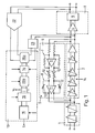
- the analog base band unit of Fig. 1 is part of a RF receiver also comprising an analog front end and a digital base band unit as well as auxiliary components as is well known in the art.
- the input receiving the output signal of a mixer is directly connected to a cascaded low pass filter 1.
- Low pass filter 1 has variable properties, so it can be calibrated to provide compensation for component tolerances and adapted to the chosen mode of operation.
- Its output is connected to the input of a variable gain amplifier unit 2 in the shape of an amplifier chain made up of series connected amplifiers at least part of which are controllable with respect to gain.
- controllable amplifiers Gilbert cells or amplification cells with operational amplifiers may be employed. This will ensure high gain and control range, low phase noise and coherent amplification as required.
- variable gain amplifier unit 2 is followed by an A/D converter 3 consisting of a sampler 4 and a quantizer 5.
- a reverse path unit 6 connects the output of variable gain amplifier unit 2 to its input, thus completing a feedback circuit containing the latter. It comprises an inverter network 7, followed by a tunable filter network 8.
- the inverter network 7 comprises a local feedback loop with an operational amplifier 9 and resistors in the local feedback loop as well as in series with the operational amplifiers.
- the filter network 8 comprises controllable variable resistances 10 in series with another feedback loop comprising an operational amplifier 11 with feedback via controllable variable capacitances 12.
- variable gain amplifier unit 2 provides a feedback circuit offering variable gain amplification and at the same time controllable and adaptable suppression of DC and low frequency components.
- control unit 13 For the purpose of controlling variable amplifier unit 2 and reverse path unit 6 a control unit 13 is provided which comprises an integrator 14 in series with a quantizer 15 for converting the output signal of integrator 14 to a digital signal and a decoder 16 for processing the same further to produce control signals for adapting the variable resistances 10 and variable capacitances 12 of reverse path unit 6.
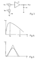
- the integrator 14 comprises (Fig. 3) a transconductance 17, whose output is connected to ground via a condensor 18. Via a speed-up input 19 a signal can be applied which is added to the input voltage. If a speed-up signal in the shape of a pulsed negative speed-up voltage V s is applied the operation point of the loop is changed and excess charge removed from condenser 18. As a consequence, the settling time of the gain control loop is reduced. This feature provides short attack time and high dynamic range of the gain control for modes of operation where this is required.
- Control unit 13 also comprises a first switchable selector 20a connecting one of two inputs to the input of integrator 14.
- a first input of selector 20a is connected to the output of a first monitoring unit, a synchronous AM detector 21 connected to the output of the variable gain amplifier unit 2.
- a second input of first selector 20a is connected to the output of a second monitoring unit, a control logic 22, e. g., a D/A converter to which the output signal of A/D converter 3 is fed.
- a second switchable selector 20b either connects the output of integrator 14 to the input of quantizer 15 or transmits a signal from the digital base band (not shown) to the same.
- the output voltage V c of second selector 20b is used as a gain control signal controlling the gain of variable gain amplifier unit 2.
- Synchronous AM detector 21 comprises a full-wave rectifier and, optionally, a one-pole low pass filter.
- Control logic 22 can have high or low resolution according to requirements. Usually, low resolution will be sufficient.
- variable resistances 10 each comprises - only the upper one will be described with reference to the drawings, the lower one being equal - a circuit containing (Fig. 2) resistors 23a-d of decreasing magnitude in parallel, each of them in series with one of switches 24a-d, as well as an additional switch 24e in parallel with resistors 23a-d. Via resistor 25 the circuit just described is connected to operational amplifier 11.
- variable capacitances 12 of filter network 8 each comprises - here again only the upper one of capacitances 12 will be described - capacitors 26a,b in parallel.
- a switch 27a controls a loop containing capacitors 26a,b whereas a further switch 27b can be used to switch single capacitor 26b, which may be external, on and off.
- Quantizer 15 (Fig. 4) comprises a series of resistors 28a-e dividing the voltage span between a higher basic reference voltage V rA and a lower basic reference voltage V rB and thereby creating four reference voltages V r1 - V r4 which are fed to the inverting inputs of four comparators 29a-d whereas the input signal, voltage V c from the output of second selector 20b which also controls variable amplifier unit 2, is fed to their non-inverting inputs in parallel.
- S 1 is high if and only if the input voltage V c of quantizer 15 is smaller than the lowest of the reference voltages V r1
- S 2 is high if and only if V c is larger than first reference voltage V r1 and smaller than second reference voltage V r2 and so on.
- S 5 is high if and only if input voltage V c is larger than the highest reference voltage, V r4 . So if the voltage V c - and, as a consequence, the gain of variable amplifier unit 2, is low - lower than V r1 - S 1 is high.
- Switches 24e, 24e' in variable resistances 10 of reverse path unit 6 are closed whereas the remaining switches there are open. The time constant of reverse path unit 6 is consequently small.
- resistors 24d, 24d', then larger resistors 24c, 24c' etc. are activated in turn which results in a rise of the time constant.
- Switches 27a, 27a' in variable capacitances 12 are controlled by the sixth digit S 6 and are normally closed.
- the sixth digit S 6 is a burst control signal corresponding to a signal B produced by the digital base band unit.
- TDMA Time Division Multiple Access
- Seventh digit S 7 controls switches 27b, 27b' whereby external capacitors 26b, 26b' can be added in parallel to capacitors 26a, 26a' to increase the time constant of reverse path unit 6.
- S 7 may be controllable directly by the user.
- the analog base band unit described above operates as follows:
- An input signal will usually contain blocking self-mixing signals which, however, are sufficiently suppressed by low pass filter unit 1.
- the resulting signal is fed to the feedback circuit made up of the variable gain amplifier unit 2 and the reverse path unit 6.
- the transfer function G(s) of variable gain amplifier unit 2 is essentially constant up to an upper cut-off frequency where it quickly falls off to zero.
- variable gain unit 2 acts as a filter suppressing in particular DC and low frequency components from blocking and local oscillator self-mixing products.
- the states of switches 24a-e, 24a'-e' and 27,a,b, 27a',b' are - in the way explained above - controlled by the reverse path control signal S produced by decoder 16 in such a way that the time constant ⁇ changes roughly proportionally with the gain G(s), which itself changes essentially proportionally with the gain control signal, voltage V c .
- H(s) the transfer function of the feedback circuit made up of variable gain amplifyer unit 2 and reverse path unit 6 is merely rescaled in proportion with the changes in the gain G(s), its shape remaining essentially constant.
- Control voltage V c is produced in a way depending on the state of selectors 20a, 20b, which depend on the chosen mode of operation. For instance, if a GPS signal is being processed, first selector 20a connects control logic 22 to the input of integrator 14 whose output is transmitted to the input of quantizer 15 by second selector 20b. The burst control and speed-up features are not used.
- the digital signal at the output of A/D converter 3 is converted back into the analog domain, fed to integrator 14 and filtered.
- the relatively slowly varying output voltage V c is then, via the second selector 20b, applied to variable gain amplifier unit 2 as gain control signal. At the same time, it is fed to quantizer 15 and controls the time constant of reverse path unit 6 via decoder 16 and the switches in filter network 8 so as to stabilize the cut-off frequency of the feedback circuit consisting of variable gain amplifier 2 and reverse path unit 6 as explained above.
- the burst control feature is activated.
- frequency hopping systems like bluetooth speed-up is active.
- variable properties of the reverse path unit 6 can additionally be exploited for a different purpose in that during processing of a GPS signal the bandwidth of the analog base band unit is adapted to the specific requirements of a signal acquisition phase and a tracking phase subsequent to acquisition of the signal, respectively.
- the carrier to noise ration y as a function of the bandwidth b (Fig. 5) has a maximum at a relatively small optimum value b 0 of the bandwidth where the pass band essentially coincides with the signal band. If the carrier to noise ratio y is at a maximum the sensitivity of the GPS receiver is optimal and search time and the probability of false alarm are small. Due to the specific properties of the GPS signal the optimum bandwidth b 0 is about 900 kHz. At higher bandwidths like b 1 the carrier to noise ratio y is considerably reduced.
- a small pre-correlation bandwidth of the system will lead to severe distortions of the correlation peak in particular where multi-path distortions are present (solid line in Fig. 6 where correlation c is shown as a function of time shift t). Consequently, it is advantageous to use a large pre-correlation bandwidth during the signal tracking phase subsequent to signal acquisition.
- a large pre-correlation bandwidth leads to a sharp peak in the correlation signal (dashed line in Fig. 6) and a correspondingly high level of the output discriminator value and allows for narrow correlation spacing. As a consequence, tracking error is low. For instance, with a pre-correlation bandwidth of 2 MHz 1-chip correlation spacing can be attained. 0.5-chip correlation spacing requires 4 MHz pre-correlation bandwidth.
- the pre-correlation bandwidth is determined by the bandwidth of the analog base band unit and can be adapted essentially by appropriately controlling reverse path unit 6.
- the specific capabilities of the analog base band unit according to the invention can be used to advantage in receivers for multiple wireless communication standards.
Landscapes
- Engineering & Computer Science (AREA)
- Power Engineering (AREA)
- Computer Networks & Wireless Communication (AREA)
- Signal Processing (AREA)
- Circuits Of Receivers In General (AREA)
Abstract
Description
- Fig. 1
- shows an overview, partly a block diagram of an analog base band unit according to the invention,
- Fig. 2
- a more detailed diagram of part of the reverse path unit of the embodiment according to Fig. 1,
- Fig. 3
- a more detailed diagram of a first part of the control unit of the embodiment according to Fig. 1,
- Fig. 4
- a more detailed diagram of a second part of the control unit of the embodiment according to Fig. 1,
- Fig. 5
- the carrier to noise ratio at the output of an analog base band unit according to the invention processing a GPS signal, as a function of its bandwidth, and
- Fig. 6
- correlation signals as functions of time shift of a GPS signal processed by an analog base band unit according to the invention, at different bandwidths.
- 1
- low pass filter unit
- 2
- variable gain amplifier unit
- 3
- A/D converter
- 4
- sampler
- 5
- quantizer
- 6
- reverse path unit
- 7
- inverter network
- 8
- filter network
- 9
- operational amplifier
- 10
- variable resistances
- 11
- operational amplifier
- 12
- variable capacitances
- 13
- control unit
- 14
- integrator
- 15
- quantizer
- 16
- decoder
- 17
- transductance
- 18
- condenser
- 19
- speed-up input
- 20a,b
- selectors
- 21
- synchronous AM detector
- 22
- logic circuit
- 23a-d, 23a'-d'
- resistors
- 24a-e, 24a'-e'
- switches
- 25, 25'
- resistors
- 26a,b, 26a',b'
- capacitors
- 27a,b, 27a',b'
- switches
- 28a-e
- resistors
- 29a-d
- comparators
Claims (22)
- Analog base band unit for a RF receiver with a feedback circuit comprising a variable gain amplifier unit (2) whose gain is set depending on a gain control signal derived from its output signal and a reverse path unit (6) connecting the output of the variable gain amplifier unit (2) with its input, characterized in that it further comprises a control unit (13) for controlling at least one time constant of the reverse path unit (6) dependent on the gain.
- Analog base band unit according to claim 1, characterized in that the at least one time constant is controllable in such a way that it varies approximately proportionally with the gain.
- Analog base band unit according to claim 1 or 2, characterized in that the variable gain amplifier unit (2) is a variable gain amplifier chain made up of Gilbert cells or of amplification cells comprising operational amplifiers and switching networks.
- Analog base band unit according to one of claims 1 to 3, characterized in that the reverse path unit (6) comprises a filter network (8) defining the at least one time constant of the reverse path unit (6).
- Analog base band unit according to claim 4, characterized in that the filter network (8) comprises at least one variable resistance (10) controllable by the control unit (13).
- Analog base band unit according to claim 5, characterized in that the variable resistance (10) comprises several resistors (23a-23d, 23a'-23d'), at least part of them each in series with at least one switch (24a-e, 24a'-e') controllable by the control unit (13).
- Analog base band unit according to one of claims 4 to 6, characterized in that the filter network (8) comprises at least one variable capacitance (12) controllable by the control unit (13).
- Analog base band unit according to claim 7, characterized in that the at least one variable capacitance (12) comprises several capacitors (26a, 26b, 26a', 26b'), at least part of them in series each with at least one switch (27a, 27b, 27a', 27b') controllable by the control unit (13).
- Analog base band unit according to claim 7 or 8, characterized in that the variable capacitance (12) is part of a local feedback loop comprising an operational amplifier (11).
- Analog base band unit according to one of claims 1 to 9, characterized in that the control unit (13) comprises a quantizer (15) comparing an input signal voltage (Vc) with several reference voltages (Vr1-Vr4) and providing digital output signals (A1-A4), each reflecting the result of one of the voltage comparisons and a decoder (16) for processing the said digital signals to provide at least part of a reverse path control signal (S) for controlling the time constant of the reverse path unit (6).
- Analog base band unit according to one of claims 1 to 10, characterized in that the control unit (13) comprises an integrator (14).
- Analog base band unit according to claim 11, characterized in that the integrator (14) has a speed-up input (19) for receiving a speed-up signal.
- Analog base band unit according to one of claims 1 to 12, characterized in that it comprises a selector (20a) for connecting one of several inputs of the control unit (13) to further components of the same.
- Analog base band unit according to claim 13, characterized in that it comprises a first monitoring unit connected between the output of the variable gain amplifier unit (2) and a first input of the selector (20a).
- Analog base band unit according to claim 14, characterized in that the first monitoring unit is a synchronous AM detector (21).
- Analog base band unit according to one of claims 1 to 15, characterized in that it comprises an A/D converter (3) for converting the output signal of the variable gain amplifier unit (6) to a digital signal.
- Analog base band unit according to one of claims 13 to 15 and claim 16, characterized in that it further comprises a second monitoring unit connected between the output of the A/D converter (3) and a second input of the selector (20a).
- Analog base band unit according to claim 17, characterized in that the second monitoring unit comprises a D/A converter or a logic control unit (22).
- Analog base band unit according to one of claims 7 to 18, characterized in that it comprises at least one switch (27a, 27a') controllable by a burst control signal to shut off the at least one variable capacitance (12) in the reverse path unit (6).
- Analog base band unit according to one of claims 1 to 19, characterized in that it comprises a low pass filter unit (1) preceding the variable gain amplifier unit (2).
- Method for using an analog base band unit according to one of claims 1 to 20 to process a GPS signal, characterized in that the analog base band unit is controlled so as to process the signal with an acquisition bandwidth during a signal acquisition phase and with a larger tracking bandwidth during a subsequent signal tracking phase.
- Method according to claim 21, characterized in that the tracking bandwidth is at least twice the acquisition bandwidth.
Priority Applications (1)
| Application Number | Priority Date | Filing Date | Title |
|---|---|---|---|
| EP20020405501 EP1271770B1 (en) | 2001-06-19 | 2002-06-18 | Analog base band unit for RF receiver and method for using the same |
Applications Claiming Priority (3)
| Application Number | Priority Date | Filing Date | Title |
|---|---|---|---|
| EP01810598A EP1271768A1 (en) | 2001-06-19 | 2001-06-19 | Analog base band unit for a RF receiver |
| EP01810598 | 2001-06-19 | ||
| EP20020405501 EP1271770B1 (en) | 2001-06-19 | 2002-06-18 | Analog base band unit for RF receiver and method for using the same |
Publications (3)
| Publication Number | Publication Date |
|---|---|
| EP1271770A2 true EP1271770A2 (en) | 2003-01-02 |
| EP1271770A3 EP1271770A3 (en) | 2006-09-13 |
| EP1271770B1 EP1271770B1 (en) | 2008-08-06 |
Family
ID=26077390
Family Applications (1)
| Application Number | Title | Priority Date | Filing Date |
|---|---|---|---|
| EP20020405501 Expired - Lifetime EP1271770B1 (en) | 2001-06-19 | 2002-06-18 | Analog base band unit for RF receiver and method for using the same |
Country Status (1)
| Country | Link |
|---|---|
| EP (1) | EP1271770B1 (en) |
Cited By (1)
| Publication number | Priority date | Publication date | Assignee | Title |
|---|---|---|---|---|
| CN110474612A (en) * | 2019-05-31 | 2019-11-19 | 华润半导体(深圳)有限公司 | A kind of variable gain amplifier, application method and bio signal handle chip |
Family Cites Families (4)
| Publication number | Priority date | Publication date | Assignee | Title |
|---|---|---|---|---|
| ZA95605B (en) * | 1994-04-28 | 1995-12-20 | Qualcomm Inc | Method and apparatus for automatic gain control and dc offset cancellation in quadrature receiver |
| US5471665A (en) * | 1994-10-18 | 1995-11-28 | Motorola, Inc. | Differential DC offset compensation circuit |
| US5901347A (en) * | 1996-01-17 | 1999-05-04 | Motorola, Inc. | Fast automatic gain control circuit and method for zero intermediate frequency receivers and radiotelephone using same |
| US6031878A (en) * | 1997-02-28 | 2000-02-29 | Maxim Integrated Products, Inc. | Direct-conversion tuner integrated circuit for direct broadcast satellite television |
-
2002
- 2002-06-18 EP EP20020405501 patent/EP1271770B1/en not_active Expired - Lifetime
Cited By (1)
| Publication number | Priority date | Publication date | Assignee | Title |
|---|---|---|---|---|
| CN110474612A (en) * | 2019-05-31 | 2019-11-19 | 华润半导体(深圳)有限公司 | A kind of variable gain amplifier, application method and bio signal handle chip |
Also Published As
| Publication number | Publication date |
|---|---|
| EP1271770B1 (en) | 2008-08-06 |
| EP1271770A3 (en) | 2006-09-13 |
Similar Documents
| Publication | Publication Date | Title |
|---|---|---|
| JP3021662B2 (en) | Method and apparatus for automatic gain control and DC offset cancellation in a quadrature receiver | |
| JP3457325B2 (en) | Automatic gain control method and apparatus in digital receiver | |
| US8054913B2 (en) | Receiver | |
| EP2137827B1 (en) | Phase-locked loop based controller for adjusting an adaptive continuous-time filter | |
| US5901347A (en) | Fast automatic gain control circuit and method for zero intermediate frequency receivers and radiotelephone using same | |
| US6373907B1 (en) | Wireless terminal device | |
| US7372925B2 (en) | Wireless LAN receiver with I and Q RF and baseband AGC loops and DC offset cancellation | |
| US20050070325A1 (en) | System and method for digital radio receiver | |
| MXPA96005108A (en) | Method and apparatus for automatic control deganance in a digi receiver | |
| US6757340B1 (en) | Radio receiver and method for preloading an average DC-offset into a channel filter | |
| US7065336B2 (en) | Analog base band unit for a RF receiver and method for using the same | |
| EP1743418A2 (en) | Direct current offset correction systems and methods | |
| WO2002014889A2 (en) | Apparatus and method for integrated frequency hopping and gps receiver | |
| US8428543B2 (en) | Receiver arrangement with AC coupling | |
| US6324389B1 (en) | Method and circuit arrangement for processing a received signal | |
| WO2005036765A1 (en) | Envelope error extraction in if/rf feedback loops | |
| EP1271770B1 (en) | Analog base band unit for RF receiver and method for using the same | |
| US7356320B2 (en) | Apparatus and method for removing DC offset in a frequency direct-conversion device | |
| US7409198B2 (en) | Wideband variable gain amplifier in an ultra wideband receiver | |
| US20060276153A1 (en) | DC cancellation in zero-IF receivers | |
| JP2001028552A (en) | Direct conversion receiver | |
| JPH09252324A (en) | Frequency converter | |
| US20050258897A1 (en) | Amplifier arrangement and method for the compensation of a signal component in an amplifier arrangement | |
| KR20030029247A (en) | Loop filter circuit in is-95c dual mode terminal |
Legal Events
| Date | Code | Title | Description |
|---|---|---|---|
| PUAI | Public reference made under article 153(3) epc to a published international application that has entered the european phase |
Free format text: ORIGINAL CODE: 0009012 |
|
| AK | Designated contracting states |
Kind code of ref document: A2 Designated state(s): AT BE CH CY DE DK ES FI FR GB GR IE IT LI LU MC NL PT SE TR |
|
| AX | Request for extension of the european patent |
Free format text: AL;LT;LV;MK;RO;SI |
|
| RAP1 | Party data changed (applicant data changed or rights of an application transferred) |
Owner name: U-BLOX AG |
|
| PUAL | Search report despatched |
Free format text: ORIGINAL CODE: 0009013 |
|
| AK | Designated contracting states |
Kind code of ref document: A3 Designated state(s): AT BE CH CY DE DK ES FI FR GB GR IE IT LI LU MC NL PT SE TR |
|
| AX | Request for extension of the european patent |
Extension state: AL LT LV MK RO SI |
|
| RIC1 | Information provided on ipc code assigned before grant |
Ipc: H03G 3/20 20060101ALI20060807BHEP Ipc: H04L 25/06 20060101ALI20060807BHEP Ipc: H03G 3/30 20060101AFI20021023BHEP Ipc: H03F 3/45 20060101ALI20060807BHEP |
|
| 17P | Request for examination filed |
Effective date: 20070126 |
|
| AKX | Designation fees paid |
Designated state(s): AT BE CH CY DE DK ES FI FR GB GR IE IT LI LU MC NL PT SE TR |
|
| GRAP | Despatch of communication of intention to grant a patent |
Free format text: ORIGINAL CODE: EPIDOSNIGR1 |
|
| GRAS | Grant fee paid |
Free format text: ORIGINAL CODE: EPIDOSNIGR3 |
|
| GRAA | (expected) grant |
Free format text: ORIGINAL CODE: 0009210 |
|
| AK | Designated contracting states |
Kind code of ref document: B1 Designated state(s): AT BE CH CY DE DK ES FI FR GB GR IE IT LI LU MC NL PT SE TR |
|
| REG | Reference to a national code |
Ref country code: GB Ref legal event code: FG4D |
|
| REG | Reference to a national code |
Ref country code: CH Ref legal event code: EP |
|
| REG | Reference to a national code |
Ref country code: IE Ref legal event code: FG4D |
|
| REF | Corresponds to: |
Ref document number: 60228025 Country of ref document: DE Date of ref document: 20080918 Kind code of ref document: P |
|
| REG | Reference to a national code |
Ref country code: CH Ref legal event code: NV Representative=s name: ZIMMERLI, WAGNER & PARTNER AG |
|
| REG | Reference to a national code |
Ref country code: SE Ref legal event code: TRGR |
|
| REG | Reference to a national code |
Ref country code: ES Ref legal event code: FG2A Ref document number: 2311586 Country of ref document: ES Kind code of ref document: T3 |
|
| PG25 | Lapsed in a contracting state [announced via postgrant information from national office to epo] |
Ref country code: DK Free format text: LAPSE BECAUSE OF FAILURE TO SUBMIT A TRANSLATION OF THE DESCRIPTION OR TO PAY THE FEE WITHIN THE PRESCRIBED TIME-LIMIT Effective date: 20080806 |
|
| PG25 | Lapsed in a contracting state [announced via postgrant information from national office to epo] |
Ref country code: PT Free format text: LAPSE BECAUSE OF FAILURE TO SUBMIT A TRANSLATION OF THE DESCRIPTION OR TO PAY THE FEE WITHIN THE PRESCRIBED TIME-LIMIT Effective date: 20090106 |
|
| PLBE | No opposition filed within time limit |
Free format text: ORIGINAL CODE: 0009261 |
|
| STAA | Information on the status of an ep patent application or granted ep patent |
Free format text: STATUS: NO OPPOSITION FILED WITHIN TIME LIMIT |
|
| 26N | No opposition filed |
Effective date: 20090507 |
|
| REG | Reference to a national code |
Ref country code: CH Ref legal event code: PFA Owner name: U-BLOX AG Free format text: U-BLOX AG#ZUERCHERSTRASSE 68#8800 THALWIL (CH) -TRANSFER TO- U-BLOX AG#ZUERCHERSTRASSE 68#8800 THALWIL (CH) |
|
| PG25 | Lapsed in a contracting state [announced via postgrant information from national office to epo] |
Ref country code: MC Free format text: LAPSE BECAUSE OF NON-PAYMENT OF DUE FEES Effective date: 20090630 |
|
| PG25 | Lapsed in a contracting state [announced via postgrant information from national office to epo] |
Ref country code: GR Free format text: LAPSE BECAUSE OF FAILURE TO SUBMIT A TRANSLATION OF THE DESCRIPTION OR TO PAY THE FEE WITHIN THE PRESCRIBED TIME-LIMIT Effective date: 20081107 |
|
| PG25 | Lapsed in a contracting state [announced via postgrant information from national office to epo] |
Ref country code: LU Free format text: LAPSE BECAUSE OF NON-PAYMENT OF DUE FEES Effective date: 20090618 |
|
| PG25 | Lapsed in a contracting state [announced via postgrant information from national office to epo] |
Ref country code: TR Free format text: LAPSE BECAUSE OF FAILURE TO SUBMIT A TRANSLATION OF THE DESCRIPTION OR TO PAY THE FEE WITHIN THE PRESCRIBED TIME-LIMIT Effective date: 20080806 |
|
| PG25 | Lapsed in a contracting state [announced via postgrant information from national office to epo] |
Ref country code: CY Free format text: LAPSE BECAUSE OF FAILURE TO SUBMIT A TRANSLATION OF THE DESCRIPTION OR TO PAY THE FEE WITHIN THE PRESCRIBED TIME-LIMIT Effective date: 20080806 |
|
| REG | Reference to a national code |
Ref country code: CH Ref legal event code: NV Representative=s name: WAGNER PATENT AG, CH |
|
| PGFP | Annual fee paid to national office [announced via postgrant information from national office to epo] |
Ref country code: IE Payment date: 20140625 Year of fee payment: 13 Ref country code: GB Payment date: 20140618 Year of fee payment: 13 |
|
| PGFP | Annual fee paid to national office [announced via postgrant information from national office to epo] |
Ref country code: SE Payment date: 20140618 Year of fee payment: 13 Ref country code: CH Payment date: 20140618 Year of fee payment: 13 Ref country code: AT Payment date: 20140611 Year of fee payment: 13 Ref country code: IT Payment date: 20140624 Year of fee payment: 13 Ref country code: ES Payment date: 20140627 Year of fee payment: 13 Ref country code: FI Payment date: 20140611 Year of fee payment: 13 Ref country code: NL Payment date: 20140618 Year of fee payment: 13 |
|
| PGFP | Annual fee paid to national office [announced via postgrant information from national office to epo] |
Ref country code: BE Payment date: 20140620 Year of fee payment: 13 |
|
| PG25 | Lapsed in a contracting state [announced via postgrant information from national office to epo] |
Ref country code: FI Free format text: LAPSE BECAUSE OF NON-PAYMENT OF DUE FEES Effective date: 20150618 Ref country code: IT Free format text: LAPSE BECAUSE OF NON-PAYMENT OF DUE FEES Effective date: 20150618 |
|
| REG | Reference to a national code |
Ref country code: CH Ref legal event code: PL |
|
| REG | Reference to a national code |
Ref country code: SE Ref legal event code: EUG |
|
| REG | Reference to a national code |
Ref country code: AT Ref legal event code: MM01 Ref document number: 403969 Country of ref document: AT Kind code of ref document: T Effective date: 20150618 |
|
| GBPC | Gb: european patent ceased through non-payment of renewal fee |
Effective date: 20150618 |
|
| PG25 | Lapsed in a contracting state [announced via postgrant information from national office to epo] |
Ref country code: SE Free format text: LAPSE BECAUSE OF NON-PAYMENT OF DUE FEES Effective date: 20150619 |
|
| REG | Reference to a national code |
Ref country code: NL Ref legal event code: MM Effective date: 20150701 |
|
| REG | Reference to a national code |
Ref country code: IE Ref legal event code: MM4A |
|
| PG25 | Lapsed in a contracting state [announced via postgrant information from national office to epo] |
Ref country code: NL Free format text: LAPSE BECAUSE OF NON-PAYMENT OF DUE FEES Effective date: 20150701 Ref country code: LI Free format text: LAPSE BECAUSE OF NON-PAYMENT OF DUE FEES Effective date: 20150630 Ref country code: GB Free format text: LAPSE BECAUSE OF NON-PAYMENT OF DUE FEES Effective date: 20150618 Ref country code: CH Free format text: LAPSE BECAUSE OF NON-PAYMENT OF DUE FEES Effective date: 20150630 Ref country code: IE Free format text: LAPSE BECAUSE OF NON-PAYMENT OF DUE FEES Effective date: 20150618 |
|
| PG25 | Lapsed in a contracting state [announced via postgrant information from national office to epo] |
Ref country code: AT Free format text: LAPSE BECAUSE OF NON-PAYMENT OF DUE FEES Effective date: 20150618 |
|
| REG | Reference to a national code |
Ref country code: FR Ref legal event code: PLFP Year of fee payment: 15 |
|
| REG | Reference to a national code |
Ref country code: ES Ref legal event code: FD2A Effective date: 20170203 |
|
| PG25 | Lapsed in a contracting state [announced via postgrant information from national office to epo] |
Ref country code: ES Free format text: LAPSE BECAUSE OF NON-PAYMENT OF DUE FEES Effective date: 20150619 |
|
| REG | Reference to a national code |
Ref country code: FR Ref legal event code: PLFP Year of fee payment: 16 |
|
| PG25 | Lapsed in a contracting state [announced via postgrant information from national office to epo] |
Ref country code: BE Free format text: LAPSE BECAUSE OF NON-PAYMENT OF DUE FEES Effective date: 20150630 |
|
| REG | Reference to a national code |
Ref country code: FR Ref legal event code: PLFP Year of fee payment: 17 |
|
| PGFP | Annual fee paid to national office [announced via postgrant information from national office to epo] |
Ref country code: FR Payment date: 20200619 Year of fee payment: 19 Ref country code: DE Payment date: 20200618 Year of fee payment: 19 |
|
| REG | Reference to a national code |
Ref country code: DE Ref legal event code: R119 Ref document number: 60228025 Country of ref document: DE |
|
| PG25 | Lapsed in a contracting state [announced via postgrant information from national office to epo] |
Ref country code: DE Free format text: LAPSE BECAUSE OF NON-PAYMENT OF DUE FEES Effective date: 20220101 |
|
| PG25 | Lapsed in a contracting state [announced via postgrant information from national office to epo] |
Ref country code: FR Free format text: LAPSE BECAUSE OF NON-PAYMENT OF DUE FEES Effective date: 20210630 |