EP1271650B1 - Memory array and manufacturing method - Google Patents
Memory array and manufacturing method Download PDFInfo
- Publication number
- EP1271650B1 EP1271650B1 EP02254311A EP02254311A EP1271650B1 EP 1271650 B1 EP1271650 B1 EP 1271650B1 EP 02254311 A EP02254311 A EP 02254311A EP 02254311 A EP02254311 A EP 02254311A EP 1271650 B1 EP1271650 B1 EP 1271650B1
- Authority
- EP
- European Patent Office
- Prior art keywords
- electrodes
- layer
- memory
- diodes
- trenches
- Prior art date
- Legal status (The legal status is an assumption and is not a legal conclusion. Google has not performed a legal analysis and makes no representation as to the accuracy of the status listed.)
- Expired - Fee Related
Links
Images


Classifications
-
- H—ELECTRICITY
- H10—SEMICONDUCTOR DEVICES; ELECTRIC SOLID-STATE DEVICES NOT OTHERWISE PROVIDED FOR
- H10B—ELECTRONIC MEMORY DEVICES
- H10B12/00—Dynamic random access memory [DRAM] devices
-
- H—ELECTRICITY
- H01—ELECTRIC ELEMENTS
- H01L—SEMICONDUCTOR DEVICES NOT COVERED BY CLASS H10
- H01L27/00—Devices consisting of a plurality of semiconductor or other solid-state components formed in or on a common substrate
- H01L27/02—Devices consisting of a plurality of semiconductor or other solid-state components formed in or on a common substrate including semiconductor components specially adapted for rectifying, oscillating, amplifying or switching and having at least one potential-jump barrier or surface barrier; including integrated passive circuit elements with at least one potential-jump barrier or surface barrier
- H01L27/04—Devices consisting of a plurality of semiconductor or other solid-state components formed in or on a common substrate including semiconductor components specially adapted for rectifying, oscillating, amplifying or switching and having at least one potential-jump barrier or surface barrier; including integrated passive circuit elements with at least one potential-jump barrier or surface barrier the substrate being a semiconductor body
- H01L27/10—Devices consisting of a plurality of semiconductor or other solid-state components formed in or on a common substrate including semiconductor components specially adapted for rectifying, oscillating, amplifying or switching and having at least one potential-jump barrier or surface barrier; including integrated passive circuit elements with at least one potential-jump barrier or surface barrier the substrate being a semiconductor body including a plurality of individual components in a repetitive configuration
- H01L27/102—Devices consisting of a plurality of semiconductor or other solid-state components formed in or on a common substrate including semiconductor components specially adapted for rectifying, oscillating, amplifying or switching and having at least one potential-jump barrier or surface barrier; including integrated passive circuit elements with at least one potential-jump barrier or surface barrier the substrate being a semiconductor body including a plurality of individual components in a repetitive configuration including bipolar components
- H01L27/1021—Devices consisting of a plurality of semiconductor or other solid-state components formed in or on a common substrate including semiconductor components specially adapted for rectifying, oscillating, amplifying or switching and having at least one potential-jump barrier or surface barrier; including integrated passive circuit elements with at least one potential-jump barrier or surface barrier the substrate being a semiconductor body including a plurality of individual components in a repetitive configuration including bipolar components including diodes only
Definitions
- the present invention pertains to the field of memory cell arrays, preferably to memory structure and fabrication processes for reducing crosstalk between memory cells in a cross point memory array.
- Portable consumer devices are becoming more compact yet increasingly sophisticated, requiring inherent structure to generate and/or utilize increasing quantities of data.
- Digital devices such as digital cameras, may require at least hundreds of megabytes (MB) of data storage either built into or attachable to the camera.
- MB megabytes
- future storage memories should be relatively low in cost, extremely compact and have capacities of around 100 MB to one gigabyte (GB).
- the storage memory should also be low in power consumption, less than one watt, and have relatively rugged physical characteristics to cope with the portable battery-powered operating environment.
- the memory For archival storage, data need only be written to the memory once.
- the memory should have a short access time, on the order of milliseconds, and a moderate transfer rate, such as one to two MB per second.
- the storage memory should be capable of interfacing with a wide variety of industry standard platforms and modules.
- cross point memory arrays a matrix of memory elements are formed, each comprising a fuse or anti-fuse and a diode connected in series.
- the memory elements are formed by a plurality of semiconductor and passivation layers disposed between conductive lines or electrodes. Such memory elements are for example described in EP 680 087 A and in US 6 034 882 A.
- the memory system disclosed therein referred to as portable inexpensive rugged memory (PIRM), provides high capacity write-once memory at low cost for archival storage. This result is realized in part by avoiding silicon substrates, minimizing process complexity and lowering area density.
- the memory system includes a memory module formed of a laminated stack of integrated circuit layers constructed on plastic substrates. Each layer contains a cross-point diode memory array. Sensing of the data stored in the array is carried out from a separate integrated circuit remote from the memory module.
- PIRM memory is relatively inexpensive, users will likely accumulate a large number of PIRM modules with a variety of stored content. It is important to be able to fabricate and assemble memory modules by a straightforward and relatively inexpensive process to minimize the need for precision while maximizing information storage density and simplifying addressing, reading and writing functions.
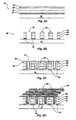
- FIG 1 three schematic diagrams illustrate likely paths for leakage current, where the cross point diodes are formed by orthogonal electrode strips having amorphous silicon p-i-n layers between the strips and the anti-fuse is made by interfacing intrinsic amorphorous silicon with a metal with the ability to diffuse into the semiconductor to form a good contact, a "diffusive metal".
- a grid of cross point memory electrodes 10 is shown.
- the bottom electrode strips 12-14 in the X direction are orthogonal to the top electrode strips 15-17 in the Y direction.
- the bottom electrode strips 12 to 14 are made of a conducting material, preferably metal, and the top electrode strips 15-17 are made of diffusive metal, such as silver. Alternate positive voltages, + V, and negative voltages, - V, are imposed on alternate electrode strips in both directions, as shown.
- Figure 1B is a cross-sectional view along the X axis of the central bottom X electrode 13 having a negative voltage, - V thereon.
- Top electrode 15 has negative voltage - V voltage
- electrode 16 has a positive voltage
- + V voltage
- electrode 17 has a negative voltage, - V.
- Diodes 20-22 are formed between electrodes 15-17 and electrode 13 by three semiconductor p-i-n layers 23-25 deposited on electrode 13.
- a p + -doped layer 23 is deposited above an intrinsic i layer 24 which in turn overlays a n + -doped layer 25.
- Anti-fuses 26-28 are formed by a passivation layer 29 formed above diodes 20-22 and beneath the top electrodes 15-17.
- a p + -doped layer is a semiconductor material such as silicon heavily doped with a p-type dopant, such as boron.
- an n + -doped layer is a semiconductor material such as silicon that is heavily doped with an n-type dopant, such as phosphorous.
- the "+" designation indicates that the material has been heavily doped to at least 1% concentration.
- Bit-to-bit crosstalk occurs when an anti-fuse of an addressed element is open (without conducting connection) while a neighboring anti-fuse is conducting.
- One leakage path is from a conducting anti-fuse to the nearest neighbor diode.
- FIG. 1B when anti-fuse 26 is conducting, a leakage current 25 flows from anti-fuse 26 through the p+-layer 23 to neighboring diode 21.
- the leakage current through the p+-layer is small since the p + -layer is usually very thin, on the order of 20 nanometers.
- Figure 1C is a cross-sectional view along the Y axis of the central top electrode 16 having a positive voltage, + V thereon.
- Bottom electrode 12 has a positive voltage, + V
- electrode 13 has a negative voltage, - V
- electrode 14 has a positive voltage, + V, imposed thereon.
- Anti-fuses 31-33 are formed by electrode 16 and passivation layer 29.
- Diodes 34-36 are formed by p-i-n layers 23-25 and electrodes 12-14. When anti-fuse 31 is conducting, leakage current 37 can flow through p+-layer 23 to neighboring diode element 35. Again, since the p+-layer 23 is quite thin, the leakage current 37 is small.
- the leakage current 38 through the n + layer 24, from electrode 14 of diode 34 to electrode 13 of diode 35, is large and can be a significant factor.
- the n-type layers are usually thicker and have substantially less resistance than p + layers.
- electron mobility is greater than hole mobility, so current leakage is usually greater in n + -layers than in p + -layers.
- FIG. 2 shows a graph giving estimated leakage current (1.E-0X means 10 -x amps) as a function of memory array size (1.E+0Y means 10 +y bits of memory).
- the estimations in the graph assume that the resistivity of phosphorous-doped amorphous silicon is about one kilo-ohm centimeter (K ⁇ -cm), the thickness of the n + layer is 100 nanometers, the voltage differences across the electrodes is 5 volts, and the line width equals the line spacing.
- K ⁇ -cm the resistivity of phosphorous-doped amorphous silicon
- the thickness of the n + layer is 100 nanometers
- the voltage differences across the electrodes is 5 volts
- the line width equals the line spacing.
- the leakage current is greater than 0.1 milliamp (10 -4 amps), which is unacceptable for a memory array.
- This point 39 is illustrated in Figure 2 at point 39.
- thin film fabrication means using a layer of semiconductor and associated barrier and conductive layers, less than or equal to a few micrometers in thickness, to build memory array devices.
- These thin film devices involve fabrication of memory cells on very thin substrates such as glass or plastic sheets, where isolation trenches in the substrate are not possible. Under such conditions, new methods and forms of fabrication are needed to minimize the crosstalk problem, which substantially increases with larger and more dense memory arrays.
- the present invention seeks to provide an improved memory array.
- Preferred embodiments can provide a cross point thin-film memory structure and fabrication process which minimize current leakage or crosstalk between memory cells.
- Such structure can be simple and easily constructed, preferably without additional critical steps or masking in the fabrication process.
- Isolation structures for thin-film memory cells can also be realized using simple, low-cost fabrication that is compatible with large-area processing and high density memory construction.
- the preferred embodiment provides a cross point memory array structure that implements a trench arrangement between adjacent rows of memory cells to provide isolation and minimize leakage current.
- a passivation material may be deposited in the trenches to increase the isolation between memory cell rows.
- the memory cells are preferably fabricated to each have a diode and anti-fuse in series between transverse electrodes. As used herein, "transverse electrodes" means electrodes that intersect at some non-zero angle.
- the trenches are constructed between memory cell rows, with the trench depth preferably extending to the bottom of the n + -layer.
- the cells may be fabricated with the anti-fuse above a diode and the passivation material from the anti-fuse may extend into the trenches to provide the isolation material.
- the diode may be constructed above the anti-fuse so that the n + -layer is higher, to minimize the trench depth.
- the trenches are cut as part of the usual etching steps for conductors, so that no additional patterning steps are necessary.
- the masking and etching processes are non-critical in nature, as described earlier.
- a cross point memory array is fabricated on a substrate and has a plurality of memory cells, each memory cell including a diode and an anti-fuse.
- a first conducting material is disposed in separated discrete areas on the substrate to form a plurality of first electrodes.
- a second conducting material is disposed in separated discrete areas that are transverse to the discrete areas of the first electrodes and are spaced from the first electrodes to form a plurality of second electrodes having cross points relative to the first electrodes.
- a plurality of semiconductor layers are disposed between the first and second electrodes to form a plurality of diodes between the cross points of the first and second electrodes.
- a passivation layer between the first electrodes and the diodes forms a plurality of anti-fuses adjacent to the diodes at the cross points of first and second electrodes. Portions of the diode layers are removed between the electrode cross points to form the plurality of memory cells with rows of trenches between adjacent memory cells to provide a barrier against crosstalk between adjacent memory cells.
- a process for fabricating a cross point memory array has a plurality of memory cells on a substrate, each memory cell including a diode and an anti-fuse.
- a first conducting material is deposited on the substrate to form a bottom electrode.
- a plurality of semiconductor layers is successively deposited over the bottom electrode. Portions of the first conducting material and the semiconductor layers are removed to form separate discrete areas of diodes and bottom electrodes extending in a first direction and having trenches extending in the first direction between adjacent diodes to provide a barrier against crosstalk between adjacent cells.
- a passivation material is deposited above the diodes along each diode discrete area and in the trenches to substantially follow the contour of the trenches.
- a second conducting material is deposited above the passivation material to form a plurality of top electrodes extending in a second direction transverse to the first direction of extension of the bottom electrodes, thereby providing the plurality of memory cells at the cross points of the top and bottom electrodes.
- a process for fabricating a cross point memory array has a plurality of memory cells on a substrate, each memory cell including a diode and an anti-fuse.
- a first conducting material is deposited on the substrate to form a bottom electrode.
- a passivation material is deposited above the first conducting material. Portions of the first conducting material and the passivation material are removed to form strips extending in a first direction along the substrate.
- a plurality of semiconductor layers is deposited successively over the passivation material.
- a second conducting material is deposited on the plurality of semiconductor layers.
- Portions of the second conducting material and the semiconductor layers are removed to form separate strips of memory cells with top electrodes extending in a second direction transverse to the first direction of the bottom electrodes, thereby forming trenches extending in the second direction between adjacent memory cells to provide a barrier against crosstalk between adjacent cells.
- a process for fabricating a cross point memory array having a plurality of memory cells on a substrate, wherein each memory cell includes a diode disposed adjacent to one line electrode.
- the process comprises etching together in one fabrication step the boundaries extending along a first direction of each of the diodes and each of the line electrodes to form multiple rows of the diodes and the one line electrode extending in the first direction.
- each memory cell comprises a diode and an anti-fuse element in series, with the anti-fuse element on top.
- fuse or anti-fuse shall refer, interchangeably, to both a fuse that is not conductive when blown and an anti-fuse that is conductive when blown.
- an anti-fuse element is preferred, but either a fuse or an anti-fuse may be used.
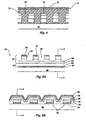
- Figure 3A shows a partially-fabricated memory array 40 consisting of three diode p-i-n layers that overlay a bottom electrode layer 42, which in turn is deposited on a substrate 41.
- n + -layer 44 is preferably thicker than p + -layer 46.
- Intrinsic layer 45 is deposited between the n + -layer and the p + -layer to provide completion of the p-i-n diode.
- the words "intrinsic layer” shall mean a layer with no intentional doping. Typical layer thicknesses are: 20 nanometers for the p + -layer, 100 nanometers for the n + -layer and 200 nanometers for the intrinsic layer.
- a memory array 50 is shown in which layers 44-46 and electrode layer 42 have been patterned, preferably by etching, to remove intermediate portions and leave spaced diode rows 54, with trenches 52, between the diode rows mounted on electrode lines 55.
- Each diode row 54 comprises a pi-n diode, as previously discussed.
- Etching is performed by defining parallel lines, preferably by optical lithographic processes or by other lithographic processes, including stamping and imprinting. The layers and metal film are then patterned. A dry etching process is preferred.
- the parallel lines can be formed by a laser ablation technique.
- a passivation layer 62 has been deposited over each diode row 54 to provide the barrier portion of the anti-fuse as well as over trenches 52 and conforming to the shape thereof. Since current leakage is very likely to occur through the sidewalls, both the sidewalls and the bottom of the trenches are covered with the passivation layer 62.
- passivation layer means a layer of material providing a significant reduction in surface current leakage.
- the passivation layer may be made of intrinsic amorphous silicon, silicon-rich silicon nitride, SiC or other such material.
- a conducting layer 64 is deposited over the passivation layer 62 including extending into the trenches 52 in the X direction.
- the conducting layer 64 may be a "diffusive metal", as previously defined, or any other suitable material.
- Conducting layer 64 and passivation layer 62 provide an anti-fuse connected in series with each of the diodes 54.
- the conducting layer 64 is patterned and etched in a direction transverse to the direction of the trenches to define discrete memory cells 66 and conductor lines 68 separated from adjacent memory cells in the Y direction.
- top and bottom electrodes are orthogonal, that is perpendicular, to each other, but the angle of intersection is not critical except as required for such purposes as packaging.
- the electrodes could be curved and still be transverse as defined herein, provided the clcctrodes insect at some angle.
- An important advantage of the preferred fabrication process is the application of only one patterning (masking) and one etching step to fabricate rows of diodes 54 and bottom electrodes 55, as shown in Figure 3B. Moreover, these masking and etching steps are "non-critical,” that is, there is no need to precisely align the etched boundaries with some other element in the array. Other non-critical patterning and etching steps are performed in masking and removing top electrode material between adjacent memory cells in the Y direction, as shown in Figure 3D. In cross point memory arrays, it is understood that there are at least two sets of patterning and etching steps to fabricate the transverse electrode areas. In the present invention, the fabrication process and resulting isolated memory cells with substantial crosstalk reduction are achieved without any additional patterning steps and without making the existing patterning and etching steps critical.
- FIG. 3A-3D Another advantage to the embodiment shown in Figures 3A-3D is the substantially complete isolation of crosstalk achieved between the diode rows 54.
- a challenge for this fabrication method is the limitation on an etching process that can produce the smallest features shown.
- FIG 4 a variation is shown to the embodiment of Figure 3.
- the same steps are followed as are shown in Figures 3A-3B.
- the passivation material 70 is deposited to cover the trenches 52 and diodes 54 completely to form a substantially planar surface 71 upon which conducting material 72 is deposited.
- this approach requires more passivation material, the fabrication process is substantially simplified by eliminating the need to etch along the contours of the trenches.
- the memory array 80 has a plurality of memory cells 91, each formed by a diode 81 and an anti-fuse 82 in series with the diode 81 being on top of the anti-fuse 82.
- the advantage to this approach is that the trenches can be cut substantially shallower. As mentioned, the trenches should have a depth that extends at least as deep as the n + layer where most of the crosstalk occurs. By placing the diode 81 above the anti-fuse 82, the depth of the trenches can be considerably shallower than in the embodiment shown in Figure 3 yet still reach a depth that is parallel with the bottom of the n + -layer.
- Figures 5A and 5B show cross-sectional views along the X and Y axis of a plurality of memory cells 91 having a "diffusive metal" 84 deposited on a substrate 85.
- a passivation layer 86 Deposited over the "diffusive metal" 1 is a passivation layer 86.
- p + -layer 87 Above the passivation layer is a subsequently deposited p + -layer 87. Patterns of separated strips are defined on the surface of the p + -layer 87.
- the sequence of etching the p + -layer 87, passivation layer 86, and "diffusive metal” 84 results in separated strips 93 of these layer-stacks, as best seen in Figure 5B.
- Deposited over the strips 93 is an intrinsic layer 88, an n + -layer 89 and a conductive layer 90. As shown, the n + -layer 89 arid the conductive layer 90 have been etched away at intervals to form rows of memory cells 91 and isolation trenches 92. The n + -layer 89 and the conductive layer 90 can be patterned at the same time.
- Etching of the conductive material 90 in the X direction is performed as previously shown in Figure 3D. Subsequently, the n + -layer 89 can be etched by a suitable agent, such as CF 4 plasma.
- the etching process for the n + -layer 89 is not critical because selective etching of the n + material over intrinsic silicon is not required. Since the thickness of the intrinsic layer 88 is probably more than 200 nanometers, a simple timing of the etch can be utilized to stop the etching in the intrinsic silicon layer 88.
- both the top metal 90 and the n + -layer 89 can be processed by laser ablation or ion milling. The etching depth can be controlled by laser energy density, etch rate or optical interferometry.
- a memory array 90 shows a variation of the structure and process of Figures 5A and 5B.
- the isolation between memory cells 91 is realized by forming a p-type region 94 between n-type strips 89.
- Doping can be achieved by a laser technique or ion shower doping process. Both techniques are large-area compatible processes and can be performed with substrates requiring low temperature exposure.
- the back-to-back diode configuration prevents lateral leakage. This approach eliminates the trench-etching step, as described with regard to Figures 5A and 5B.
Description
- The present invention pertains to the field of memory cell arrays, preferably to memory structure and fabrication processes for reducing crosstalk between memory cells in a cross point memory array.
- Portable consumer devices are becoming more compact yet increasingly sophisticated, requiring inherent structure to generate and/or utilize increasing quantities of data. Digital devices, such as digital cameras, may require at least hundreds of megabytes (MB) of data storage either built into or attachable to the camera. To satisfy the needs of this type of data storage application, future storage memories should be relatively low in cost, extremely compact and have capacities of around 100 MB to one gigabyte (GB). The storage memory should also be low in power consumption, less than one watt, and have relatively rugged physical characteristics to cope with the portable battery-powered operating environment.
- For archival storage, data need only be written to the memory once. Preferably, the memory should have a short access time, on the order of milliseconds, and a moderate transfer rate, such as one to two MB per second. Preferably, the storage memory should be capable of interfacing with a wide variety of industry standard platforms and modules.
- An application for meeting this demand involves the use of write-once cross point memory devices. In cross point memory arrays, a matrix of memory elements are formed, each comprising a fuse or anti-fuse and a diode connected in series. The memory elements are formed by a plurality of semiconductor and passivation layers disposed between conductive lines or electrodes. Such memory elements are for example described in EP 680 087 A and in US 6 034 882 A.
- One application for utilizing write-once cross point memory arrays to provide high density archival storage in portable devices is described in United States Patent Application serial number 09/875,356, filed June 6, 2001, entitled "NON-Volatile Memory", filed before the priority date of this application, and published after the filing date of this application as US-A1-2002/0196659. The memory system disclosed therein, referred to as portable inexpensive rugged memory (PIRM), provides high capacity write-once memory at low cost for archival storage. This result is realized in part by avoiding silicon substrates, minimizing process complexity and lowering area density. The memory system includes a memory module formed of a laminated stack of integrated circuit layers constructed on plastic substrates. Each layer contains a cross-point diode memory array. Sensing of the data stored in the array is carried out from a separate integrated circuit remote from the memory module.
- Because PIRM memory is relatively inexpensive, users will likely accumulate a large number of PIRM modules with a variety of stored content. It is important to be able to fabricate and assemble memory modules by a straightforward and relatively inexpensive process to minimize the need for precision while maximizing information storage density and simplifying addressing, reading and writing functions.
- In layered high-density memory modules, such as described above, the potential for current leakage or "crosstalk" between adjacent memory cells is substantially increased. This problem can result in intolerable increases in error rates and power loss as current leaks between "on" and "off" memory cells, as well as along other potential crosstalk paths.
- In Figure 1, three schematic diagrams illustrate likely paths for leakage current, where the cross point diodes are formed by orthogonal electrode strips having amorphous silicon p-i-n layers between the strips and the anti-fuse is made by interfacing intrinsic amorphorous silicon with a metal with the ability to diffuse into the semiconductor to form a good contact, a "diffusive metal". In Figure 1A, a grid of cross
point memory electrodes 10 is shown. The bottom electrode strips 12-14 in the X direction are orthogonal to the top electrode strips 15-17 in the Y direction. Thebottom electrode strips 12 to 14 are made of a conducting material, preferably metal, and the top electrode strips 15-17 are made of diffusive metal, such as silver. Alternate positive voltages, +V, and negative voltages, -V, are imposed on alternate electrode strips in both directions, as shown. - Figure 1B is a cross-sectional view along the X axis of the central
bottom X electrode 13 having a negative voltage, -V thereon.Top electrode 15 has negative voltage -V voltage,electrode 16 has a positive voltage, +V voltage andelectrode 17 has a negative voltage, -V. Diodes 20-22 are formed between electrodes 15-17 andelectrode 13 by three semiconductor p-i-n layers 23-25 deposited onelectrode 13. A p+-dopedlayer 23 is deposited above anintrinsic i layer 24 which in turn overlays a n+-doped layer 25. Anti-fuses 26-28 are formed by a passivation layer 29 formed above diodes 20-22 and beneath the top electrodes 15-17. - A p+-doped layer is a semiconductor material such as silicon heavily doped with a p-type dopant, such as boron. Similarly an n+-doped layer is a semiconductor material such as silicon that is heavily doped with an n-type dopant, such as phosphorous. The "+" designation indicates that the material has been heavily doped to at least 1% concentration.
- Bit-to-bit crosstalk occurs when an anti-fuse of an addressed element is open (without conducting connection) while a neighboring anti-fuse is conducting. One leakage path is from a conducting anti-fuse to the nearest neighbor diode. As shown in Figure 1B, when anti-fuse 26 is conducting, a leakage current 25 flows from anti-fuse 26 through the p+-
layer 23 to neighboringdiode 21. The leakage current through the p+-layer is small since the p+-layer is usually very thin, on the order of 20 nanometers. - Figure 1C is a cross-sectional view along the Y axis of the
central top electrode 16 having a positive voltage, +V thereon.Bottom electrode 12 has a positive voltage, +V,electrode 13 has a negative voltage, -V, andelectrode 14 has a positive voltage, +V, imposed thereon. Anti-fuses 31-33 are formed byelectrode 16 and passivation layer 29. Diodes 34-36 are formed by p-i-n layers 23-25 and electrodes 12-14. When anti-fuse 31 is conducting,leakage current 37 can flow through p+-layer 23 to neighboringdiode element 35. Again, since the p+-layer 23 is quite thin, theleakage current 37 is small. However, theleakage current 38 through the n+layer 24, fromelectrode 14 ofdiode 34 toelectrode 13 ofdiode 35, is large and can be a significant factor. The n-type layers are usually thicker and have substantially less resistance than p+ layers. In addition, electron mobility is greater than hole mobility, so current leakage is usually greater in n+-layers than in p+-layers. - Leakage current increases with the size of a memory array. Figure 2 shows a graph giving estimated leakage current (1.E-0X means 10-x amps) as a function of memory array size (1.E+0Y means 10+y bits of memory). The estimations in the graph assume that the resistivity of phosphorous-doped amorphous silicon is about one kilo-ohm centimeter (KΩ-cm), the thickness of the n+ layer is 100 nanometers, the voltage differences across the electrodes is 5 volts, and the line width equals the line spacing. When the size of a memory array exceeds one megabit (10+6 memory cells), the leakage current is greater than 0.1 milliamp (10-4 amps), which is unacceptable for a memory array. This point is illustrated in Figure 2 at
point 39. At the present time, consumer units having at least 8 megabytes (64 megabits) of memory are not unusual. Thus, leakage current is a major problem in both existing and future memory arrays. - Others have attempted to construct various means for minimizing current leakage in memory arrays. One such structure is shown in companion patents, U.S. Patent Nos. 4,698,900 and 5,008,722 (Esquivel), in which a cross point EPROM array has trenches to provide improved isolation and improved leakage current characteristics between adjacent buried n+ bitlines. The Esquivel fabrication process involves etching a trench into a single crystal silicon substrate after surface layers have been removed. The achievement of isolating complex three terminal EPROM transistor devices has unique requirements, not easily translated to other technologies, such as the thin film construction utilized for high-density, portable, inexpensive data storage.
- Cross point memory arrays using thin film fabrication and two terminal diode devices present a greater challenge. As used herein, thin film fabrication means using a layer of semiconductor and associated barrier and conductive layers, less than or equal to a few micrometers in thickness, to build memory array devices. These thin film devices involve fabrication of memory cells on very thin substrates such as glass or plastic sheets, where isolation trenches in the substrate are not possible. Under such conditions, new methods and forms of fabrication are needed to minimize the crosstalk problem, which substantially increases with larger and more dense memory arrays.
- The present invention seeks to provide an improved memory array.
- According to an aspect of the present invention there is provided a thin-film cross point memory array as specified in claim 1.
- According to another aspect of the present invention there is provided a process of fabricating a thin film cross point memory array as specified in claim 6.
- Preferred embodiments can provide a cross point thin-film memory structure and fabrication process which minimize current leakage or crosstalk between memory cells. Such structure can be simple and easily constructed, preferably without additional critical steps or masking in the fabrication process. Isolation structures for thin-film memory cells can also be realized using simple, low-cost fabrication that is compatible with large-area processing and high density memory construction.
- The preferred embodiment provides a cross point memory array structure that implements a trench arrangement between adjacent rows of memory cells to provide isolation and minimize leakage current. A passivation material may be deposited in the trenches to increase the isolation between memory cell rows. The memory cells are preferably fabricated to each have a diode and anti-fuse in series between transverse electrodes. As used herein, "transverse electrodes" means electrodes that intersect at some non-zero angle. The trenches are constructed between memory cell rows, with the trench depth preferably extending to the bottom of the n+-layer. The cells may be fabricated with the anti-fuse above a diode and the passivation material from the anti-fuse may extend into the trenches to provide the isolation material. Alternatively, the diode may be constructed above the anti-fuse so that the n+-layer is higher, to minimize the trench depth. The trenches are cut as part of the usual etching steps for conductors, so that no additional patterning steps are necessary. Moreover, the masking and etching processes are non-critical in nature, as described earlier.
- In one embodiment of the preferred invention, a cross point memory array is fabricated on a substrate and has a plurality of memory cells, each memory cell including a diode and an anti-fuse. A first conducting material is disposed in separated discrete areas on the substrate to form a plurality of first electrodes. A second conducting material is disposed in separated discrete areas that are transverse to the discrete areas of the first electrodes and are spaced from the first electrodes to form a plurality of second electrodes having cross points relative to the first electrodes. A plurality of semiconductor layers are disposed between the first and second electrodes to form a plurality of diodes between the cross points of the first and second electrodes. A passivation layer between the first electrodes and the diodes forms a plurality of anti-fuses adjacent to the diodes at the cross points of first and second electrodes. Portions of the diode layers are removed between the electrode cross points to form the plurality of memory cells with rows of trenches between adjacent memory cells to provide a barrier against crosstalk between adjacent memory cells.
- In another preferred embodiment, a process for fabricating a cross point memory array has a plurality of memory cells on a substrate, each memory cell including a diode and an anti-fuse. A first conducting material is deposited on the substrate to form a bottom electrode. A plurality of semiconductor layers is successively deposited over the bottom electrode. Portions of the first conducting material and the semiconductor layers are removed to form separate discrete areas of diodes and bottom electrodes extending in a first direction and having trenches extending in the first direction between adjacent diodes to provide a barrier against crosstalk between adjacent cells. A passivation material is deposited above the diodes along each diode discrete area and in the trenches to substantially follow the contour of the trenches. A second conducting material is deposited above the passivation material to form a plurality of top electrodes extending in a second direction transverse to the first direction of extension of the bottom electrodes, thereby providing the plurality of memory cells at the cross points of the top and bottom electrodes.
- In another preferred embodiment, a process for fabricating a cross point memory array has a plurality of memory cells on a substrate, each memory cell including a diode and an anti-fuse. A first conducting material is deposited on the substrate to form a bottom electrode. A passivation material is deposited above the first conducting material. Portions of the first conducting material and the passivation material are removed to form strips extending in a first direction along the substrate. A plurality of semiconductor layers is deposited successively over the passivation material. A second conducting material is deposited on the plurality of semiconductor layers. Portions of the second conducting material and the semiconductor layers are removed to form separate strips of memory cells with top electrodes extending in a second direction transverse to the first direction of the bottom electrodes, thereby forming trenches extending in the second direction between adjacent memory cells to provide a barrier against crosstalk between adjacent cells.
- In another preferred embodiment, a process is provided for fabricating a cross point memory array having a plurality of memory cells on a substrate, wherein each memory cell includes a diode disposed adjacent to one line electrode. The process comprises etching together in one fabrication step the boundaries extending along a first direction of each of the diodes and each of the line electrodes to form multiple rows of the diodes and the one line electrode extending in the first direction.
- Embodiments of the present invention are described below, by way of example only, with reference to the accompanying drawings in which:
- Figures 1A-1C are schematic plans and cross-sectional views showing cross point memory devices having diodes and anti-fuses in series;
- Figure 2 is a graph illustrating the relationship between leakage current and memory array size for cross-point memory arrays;
- Figures 3A-3D are schematic side views showing fabrication steps of a preferred embodiment of cross point memory array;
- Figure 4 is a schematic view showing a variation in the embodiment of Figure 3; and
- Figures 5A, 5B and 6 are schematic side views showing alternative structures and fabrication of additional preferred embodiments of memory array.
- With reference to Figures 3A-3C, schematic illustrations of key steps in the fabrication of a cross point memory array are shown. In this embodiment each memory cell comprises a diode and an anti-fuse element in series, with the anti-fuse element on top. As used herein either of the words "fuse" or "anti-fuse" shall refer, interchangeably, to both a fuse that is not conductive when blown and an anti-fuse that is conductive when blown. In most cases, for the preferred embodiments of the present invention, an anti-fuse element is preferred, but either a fuse or an anti-fuse may be used.
- Figure 3A shows a partially-fabricated
memory array 40 consisting of three diode p-i-n layers that overlay a bottom electrode layer 42, which in turn is deposited on asubstrate 41. As mentioned previously, n+-layer 44 is preferably thicker than p+-layer 46.Intrinsic layer 45 is deposited between the n+-layer and the p+-layer to provide completion of the p-i-n diode. As used herein, the words "intrinsic layer" shall mean a layer with no intentional doping. Typical layer thicknesses are: 20 nanometers for the p+-layer, 100 nanometers for the n+-layer and 200 nanometers for the intrinsic layer. - As shown in Figure 3B, a
memory array 50 is shown in which layers 44-46 and electrode layer 42 have been patterned, preferably by etching, to remove intermediate portions and leave spaceddiode rows 54, withtrenches 52, between the diode rows mounted onelectrode lines 55. Eachdiode row 54 comprises a pi-n diode, as previously discussed. Etching is performed by defining parallel lines, preferably by optical lithographic processes or by other lithographic processes, including stamping and imprinting. The layers and metal film are then patterned. A dry etching process is preferred. As an alternative, the parallel lines can be formed by a laser ablation technique. - In Figure 3C a
passivation layer 62 has been deposited over eachdiode row 54 to provide the barrier portion of the anti-fuse as well as overtrenches 52 and conforming to the shape thereof. Since current leakage is very likely to occur through the sidewalls, both the sidewalls and the bottom of the trenches are covered with thepassivation layer 62. As used herein, "passivation layer" means a layer of material providing a significant reduction in surface current leakage. The passivation layer may be made of intrinsic amorphous silicon, silicon-rich silicon nitride, SiC or other such material. - As shown in Figure 3C, a conducting
layer 64 is deposited over thepassivation layer 62 including extending into thetrenches 52 in the X direction. The conductinglayer 64 may be a "diffusive metal", as previously defined, or any other suitable material. Conductinglayer 64 andpassivation layer 62 provide an anti-fuse connected in series with each of thediodes 54. Finally, in Figure 3D theconducting layer 64 is patterned and etched in a direction transverse to the direction of the trenches to definediscrete memory cells 66 and conductor lines 68 separated from adjacent memory cells in the Y direction. - The most common arrangement is for the top and bottom electrodes to be orthogonal, that is perpendicular, to each other, but the angle of intersection is not critical except as required for such purposes as packaging. Although the maximum packaging density is achieved by the orthogonal arrangement, the electrodes could be curved and still be transverse as defined herein, provided the clcctrodes insect at some angle.
- An important advantage of the preferred fabrication process is the application of only one patterning (masking) and one etching step to fabricate rows of
diodes 54 andbottom electrodes 55, as shown in Figure 3B. Moreover, these masking and etching steps are "non-critical," that is, there is no need to precisely align the etched boundaries with some other element in the array. Other non-critical patterning and etching steps are performed in masking and removing top electrode material between adjacent memory cells in the Y direction, as shown in Figure 3D. In cross point memory arrays, it is understood that there are at least two sets of patterning and etching steps to fabricate the transverse electrode areas. In the present invention, the fabrication process and resulting isolated memory cells with substantial crosstalk reduction are achieved without any additional patterning steps and without making the existing patterning and etching steps critical. - Another advantage to the embodiment shown in Figures 3A-3D is the substantially complete isolation of crosstalk achieved between the
diode rows 54. A challenge for this fabrication method is the limitation on an etching process that can produce the smallest features shown. - In Figure 4, a variation is shown to the embodiment of Figure 3. In this process the same steps are followed as are shown in Figures 3A-3B. Thereafter, the
passivation material 70 is deposited to cover thetrenches 52 anddiodes 54 completely to form a substantiallyplanar surface 71 upon which conductingmaterial 72 is deposited. Although this approach requires more passivation material, the fabrication process is substantially simplified by eliminating the need to etch along the contours of the trenches. - Referring now to Figures 5 and 6, another preferred embodiment of the invention is shown in which the memory array 80 has a plurality of
memory cells 91, each formed by adiode 81 and an anti-fuse 82 in series with thediode 81 being on top of the anti-fuse 82. The advantage to this approach is that the trenches can be cut substantially shallower. As mentioned, the trenches should have a depth that extends at least as deep as the n+ layer where most of the crosstalk occurs. By placing thediode 81 above the anti-fuse 82, the depth of the trenches can be considerably shallower than in the embodiment shown in Figure 3 yet still reach a depth that is parallel with the bottom of the n+-layer. - Figures 5A and 5B show cross-sectional views along the X and Y axis of a plurality of
memory cells 91 having a "diffusive metal" 84 deposited on asubstrate 85. Deposited over the "diffusive metal" 1 is a passivation layer 86. Above the passivation layer is a subsequently deposited p+-layer 87. Patterns of separated strips are defined on the surface of the p+-layer 87. The sequence of etching the p+-layer 87, passivation layer 86, and "diffusive metal" 84 results in separatedstrips 93 of these layer-stacks, as best seen in Figure 5B. Deposited over thestrips 93 is an intrinsic layer 88, an n+-layer 89 and aconductive layer 90. As shown, the n+-layer 89 arid theconductive layer 90 have been etched away at intervals to form rows ofmemory cells 91 andisolation trenches 92. The n+-layer 89 and theconductive layer 90 can be patterned at the same time. - Etching of the
conductive material 90 in the X direction is performed as previously shown in Figure 3D. Subsequently, the n+-layer 89 can be etched by a suitable agent, such as CF4 plasma. The etching process for the n+-layer 89 is not critical because selective etching of the n+ material over intrinsic silicon is not required. Since the thickness of the intrinsic layer 88 is probably more than 200 nanometers, a simple timing of the etch can be utilized to stop the etching in the intrinsic silicon layer 88. Alternately, both thetop metal 90 and the n+-layer 89 can be processed by laser ablation or ion milling. The etching depth can be controlled by laser energy density, etch rate or optical interferometry. - In Figure 6, a
memory array 90 shows a variation of the structure and process of Figures 5A and 5B. The isolation betweenmemory cells 91 is realized by forming a p-type region 94 between n-type strips 89. Doping can be achieved by a laser technique or ion shower doping process. Both techniques are large-area compatible processes and can be performed with substrates requiring low temperature exposure. Along the Y direction (into the paper), the back-to-back diode configuration prevents lateral leakage. This approach eliminates the trench-etching step, as described with regard to Figures 5A and 5B. - Other embodiments will be apparent to those skilled in the art from a consideration of this description and the appended claims, or from a practice of the disclosed embodiments.
Claims (6)
- A thin-film cross point memory array (40;80) fabricated on a substrate (41;85) and including a plurality of memory cells, each memory cell (66;91) including a diode (44,45,46;81) and an anti-fuse (62,64;82), the memory array including:a first conductive material (42;84) disposed in discrete areas on the substrate to form a plurality of first electrodes (55;93);a second conductive material (64;90) disposed in discrete areas substantially transverse to the discrete areas of the first electrodes (55;93) and spaced from the first electrodes (55;93) to form a plurality of second electrodes (64;90) having cross points relative to the first electrodes (55;93);a plurality of semiconductor (44,45,46;87,88,89) layers disposed between the first and second electrodes (55,64;93,90) to form a diode (54) between each of the cross points of the first and second electrodes (55,64;93,90); anda passivation layer (62,68) between the first electrodes (55) and the diodes (54) to form a plurality of anti-fuses adjacent the diodes (54) at the cross points of the first and second electrodes;wherein portions of the diode layers (44,45,46) are removed between adjacent electrode cross points to form the plurality of memory cells with rows of trenches (52) between adjacent memory cells to provide a barrier against cross-talk between adjacent memory cells; characterized in that:the passivation layer (62,68) is disposed in the trenches (52) between the memory cells.
- A memory array as in claim 1, wherein the plurality of semiconductor layers includes a p-doped layer (87), an n-doped layer (89) and an intrinsic layer (88) disposed between the p-doped layer (87) and the n-doped layer (89) to form the plurality of diodes (81).
- A memory array as in claim 2, wherein the depth of the trench (92) extends substantially parallel to the bottom of the n-doped layer (89).
- A memory array as in claim 2 or 3, including passivation material (94) disposed in the trenches (92) between the n-doped layers (89).
- A memory array as in any preceding claim, wherein the first electrodes (93) are disposed between the passivation layer (86) and the substrate (85) to form the anti-fuses (82) beneath the diodes (81).
- A process of fabricating a thin-film cross point memory array having a plurality of memory cells (50) on a substrate (41), each memory cell (66) including a diode (54) and an anti-fuse (62,64), including the steps of:(a) depositing a first conductive material (42) on the substrate (41) to form a bottom electrode (55);(b) depositing a plurality of semiconductor layers (44,45,46) successively over the bottom electrode (55);(c) removing portions of the first conductive material (42) and the semiconductor layers (44,45,46) to form discrete areas of diodes (54) and bottom electrodes (55) extending in a first direction and having trenches (52) extending in the first direction between adjacent diodes (54) to provide a barrier against crosstalk between adjacent cells (66); characterized by the steps: (d) depositing a passivation material (62,68) above the diodes (54) along each diode area and in the trenches (52) to follow substantially the contour of the trenches (52); and(e) depositing a second conductive material (64) above the passivation material (62) to form a plurality of top electrodes (64) extending in a second direction substantially transverse to the first direction of extension of the bottom electrodes (55), the passivation material (62,68) and the second conductive material (64) forming a plurality of anti-fuses thereby providing a plurality of memory cells (66) at the cross points of the top and bottom electrodes (64,55).
Applications Claiming Priority (2)
| Application Number | Priority Date | Filing Date | Title |
|---|---|---|---|
| US09/896,480 US6599796B2 (en) | 2001-06-29 | 2001-06-29 | Apparatus and fabrication process to reduce crosstalk in pirm memory array |
| US896480 | 2001-06-29 |
Publications (3)
| Publication Number | Publication Date |
|---|---|
| EP1271650A2 EP1271650A2 (en) | 2003-01-02 |
| EP1271650A3 EP1271650A3 (en) | 2003-12-03 |
| EP1271650B1 true EP1271650B1 (en) | 2007-04-25 |
Family
ID=25406289
Family Applications (1)
| Application Number | Title | Priority Date | Filing Date |
|---|---|---|---|
| EP02254311A Expired - Fee Related EP1271650B1 (en) | 2001-06-29 | 2002-06-20 | Memory array and manufacturing method |
Country Status (7)
| Country | Link |
|---|---|
| US (1) | US6599796B2 (en) |
| EP (1) | EP1271650B1 (en) |
| JP (1) | JP2003060162A (en) |
| KR (1) | KR20030003106A (en) |
| CN (1) | CN1395312A (en) |
| DE (1) | DE60219719T2 (en) |
| TW (1) | TW546751B (en) |
Families Citing this family (32)
| Publication number | Priority date | Publication date | Assignee | Title |
|---|---|---|---|---|
| US5673218A (en) | 1996-03-05 | 1997-09-30 | Shepard; Daniel R. | Dual-addressed rectifier storage device |
| US6956757B2 (en) * | 2000-06-22 | 2005-10-18 | Contour Semiconductor, Inc. | Low cost high density rectifier matrix memory |
| AU2001294817A1 (en) * | 2000-09-27 | 2002-04-08 | Nup2 Incorporated | Fabrication of semiconductor devices |
| DE10155023B4 (en) * | 2001-11-05 | 2008-11-06 | Qimonda Ag | Line arrangement for bit lines for contacting at least one memory cell and method for producing a line arrangement for bit lines |
| US6642603B1 (en) * | 2002-06-27 | 2003-11-04 | Matrix Semiconductor, Inc. | Same conductivity type highly-doped regions for antifuse memory cell |
| US6683365B1 (en) * | 2002-08-01 | 2004-01-27 | Micron Technology, Inc. | Edge intensive antifuse device structure |
| US6867132B2 (en) * | 2002-09-17 | 2005-03-15 | Hewlett-Packard Development Company, L.P. | Large line conductive pads for interconnection of stackable circuitry |
| US20060171200A1 (en) | 2004-02-06 | 2006-08-03 | Unity Semiconductor Corporation | Memory using mixed valence conductive oxides |
| US7082052B2 (en) | 2004-02-06 | 2006-07-25 | Unity Semiconductor Corporation | Multi-resistive state element with reactive metal |
| US7195950B2 (en) * | 2004-07-21 | 2007-03-27 | Hewlett-Packard Development Company, L.P. | Forming a plurality of thin-film devices |
| US7106639B2 (en) * | 2004-09-01 | 2006-09-12 | Hewlett-Packard Development Company, L.P. | Defect management enabled PIRM and method |
| US7110278B2 (en) * | 2004-09-29 | 2006-09-19 | Intel Corporation | Crosspoint memory array utilizing one time programmable antifuse cells |
| US7321502B2 (en) * | 2004-09-30 | 2008-01-22 | Intel Corporation | Non volatile data storage through dielectric breakdown |
| KR100593750B1 (en) * | 2004-11-10 | 2006-06-28 | 삼성전자주식회사 | Cross-point nonvolatile memory device adopting binary metal oxide film as data storage material film and manufacturing method |
| US8559209B2 (en) | 2011-06-10 | 2013-10-15 | Unity Semiconductor Corporation | Array voltage regulating technique to enable data operations on large cross-point memory arrays with resistive memory elements |
| US8270193B2 (en) | 2010-01-29 | 2012-09-18 | Unity Semiconductor Corporation | Local bit lines and methods of selecting the same to access memory elements in cross-point arrays |
| US20130082232A1 (en) | 2011-09-30 | 2013-04-04 | Unity Semiconductor Corporation | Multi Layered Conductive Metal Oxide Structures And Methods For Facilitating Enhanced Performance Characteristics Of Two Terminal Memory Cells |
| US8937292B2 (en) | 2011-08-15 | 2015-01-20 | Unity Semiconductor Corporation | Vertical cross point arrays for ultra high density memory applications |
| US8565003B2 (en) | 2011-06-28 | 2013-10-22 | Unity Semiconductor Corporation | Multilayer cross-point memory array having reduced disturb susceptibility |
| US7473986B2 (en) * | 2006-09-22 | 2009-01-06 | Taiwan Semiconductor Manufacturing Co., Ltd. | Positive-intrinsic-negative (PIN) diode semiconductor devices and fabrication methods thereof |
| US7813157B2 (en) * | 2007-10-29 | 2010-10-12 | Contour Semiconductor, Inc. | Non-linear conductor memory |
| US20090225621A1 (en) * | 2008-03-05 | 2009-09-10 | Shepard Daniel R | Split decoder storage array and methods of forming the same |
| WO2009149061A2 (en) * | 2008-06-02 | 2009-12-10 | Contour Semiconductor, Inc. | Diode decoder array with non-sequential layout and methods of forming the same |
| US8105884B2 (en) | 2008-10-06 | 2012-01-31 | Samsung Electronics Co., Ltd. | Cross point memory arrays, methods of manufacturing the same, masters for imprint processes, and methods of manufacturing masters |
| US8586962B2 (en) | 2008-10-06 | 2013-11-19 | Samsung Electronics Co., Ltd. | Cross point memory arrays, methods of manufacturing the same, masters for imprint processes, and methods of manufacturing masters |
| US8325556B2 (en) * | 2008-10-07 | 2012-12-04 | Contour Semiconductor, Inc. | Sequencing decoder circuit |
| KR101493874B1 (en) * | 2008-11-12 | 2015-02-16 | 삼성전자주식회사 | Non-volatile memory device |
| CN101752312B (en) * | 2008-12-03 | 2012-05-30 | 中国科学院上海微系统与信息技术研究所 | Manufacturing method of high-density diode array with double shallow trench isolation channels |
| US8638584B2 (en) * | 2010-02-02 | 2014-01-28 | Unity Semiconductor Corporation | Memory architectures and techniques to enhance throughput for cross-point arrays |
| US8891276B2 (en) | 2011-06-10 | 2014-11-18 | Unity Semiconductor Corporation | Memory array with local bitlines and local-to-global bitline pass gates and gain stages |
| US9117495B2 (en) | 2011-06-10 | 2015-08-25 | Unity Semiconductor Corporation | Global bit line pre-charge circuit that compensates for process, operating voltage, and temperature variations |
| US10566056B2 (en) | 2011-06-10 | 2020-02-18 | Unity Semiconductor Corporation | Global bit line pre-charge circuit that compensates for process, operating voltage, and temperature variations |
Family Cites Families (33)
| Publication number | Priority date | Publication date | Assignee | Title |
|---|---|---|---|---|
| IL61671A (en) * | 1979-12-13 | 1984-04-30 | Energy Conversion Devices Inc | Diode and rom or eeprom devices using it |
| US4423432A (en) * | 1980-01-28 | 1983-12-27 | Rca Corporation | Apparatus for decoding multiple input lines |
| US4419741A (en) * | 1980-01-28 | 1983-12-06 | Rca Corporation | Read only memory (ROM) having high density memory array with on pitch decoder circuitry |
| US4667189A (en) * | 1984-04-25 | 1987-05-19 | Energy Conversion Devices, Inc. | Programmable semiconductor switch for a display matrix or the like and method for making same |
| US5008722A (en) | 1986-03-27 | 1991-04-16 | Texas Instruments Incorporated | Non-volatile memory |
| US4698900A (en) | 1986-03-27 | 1987-10-13 | Texas Instruments Incorporated | Method of making a non-volatile memory having dielectric filled trenches |
| US4881114A (en) * | 1986-05-16 | 1989-11-14 | Actel Corporation | Selectively formable vertical diode circuit element |
| US5227660A (en) * | 1987-11-09 | 1993-07-13 | Hitachi, Ltd. | Semiconductor device |
| US5311039A (en) * | 1990-04-24 | 1994-05-10 | Seiko Epson Corporation | PROM and ROM memory cells |
| GB9113795D0 (en) * | 1991-06-26 | 1991-08-14 | Philips Electronic Associated | Thin-film rom devices and their manufacture |
| US5170243A (en) * | 1991-11-04 | 1992-12-08 | International Business Machines Corporation | Bit line configuration for semiconductor memory |
| JP3256603B2 (en) * | 1993-07-05 | 2002-02-12 | 株式会社東芝 | Semiconductor device and manufacturing method thereof |
| US5362665A (en) * | 1994-02-14 | 1994-11-08 | Industrial Technology Research Institute | Method of making vertical DRAM cross point memory cell |
| GB9404113D0 (en) * | 1994-03-03 | 1994-04-20 | Philips Electronics Uk Ltd | A charge storage device |
| GB9404111D0 (en) * | 1994-03-03 | 1994-04-20 | Philips Electronics Uk Ltd | A charge storage device |
| JP3501416B2 (en) * | 1994-04-28 | 2004-03-02 | 忠弘 大見 | Semiconductor device |
| US5903041A (en) * | 1994-06-21 | 1999-05-11 | Aptix Corporation | Integrated two-terminal fuse-antifuse and fuse and integrated two-terminal fuse-antifuse structures incorporating an air gap |
| SE9500013D0 (en) * | 1995-01-03 | 1995-01-03 | Abb Research Ltd | Semiconductor device having a passivation layer |
| US5901065A (en) * | 1996-02-07 | 1999-05-04 | Motorola, Inc. | Apparatus and method for automatically placing ties and connection elements within an integrated circuit |
| US5736433A (en) * | 1996-05-22 | 1998-04-07 | Sgs-Thomson Microelectronics, Inc. | Double mask hermetic passivation method providing enhanced resistance to moisture |
| DE69734050T2 (en) * | 1996-06-05 | 2006-06-08 | Koninklijke Philips Electronics N.V. | DESCRIBABLE FIRM MEMORY ELEMENT AND THE MANUFACTURING METHOD FOR SUCH A BUILDING ELEMENT |
| US5835396A (en) * | 1996-10-17 | 1998-11-10 | Zhang; Guobiao | Three-dimensional read-only memory |
| US6028324A (en) * | 1997-03-07 | 2000-02-22 | Taiwan Semiconductor Manufacturing Company | Test structures for monitoring gate oxide defect densities and the plasma antenna effect |
| US6169686B1 (en) * | 1997-11-20 | 2001-01-02 | Hewlett-Packard Company | Solid-state memory with magnetic storage cells |
| US5991193A (en) * | 1997-12-02 | 1999-11-23 | International Business Machines Corporation | Voltage biasing for magnetic ram with magnetic tunnel memory cells |
| US6255671B1 (en) * | 1998-01-05 | 2001-07-03 | International Business Machines Corporation | Metal embedded passivation layer structure for microelectronic interconnect formation, customization and repair |
| US6174767B1 (en) * | 1998-05-11 | 2001-01-16 | Vanguard International Semiconductor Corporation | Method of fabrication of capacitor and bit-line at same level for 8F2 DRAM cell with minimum bit-line coupling noise |
| US6034882A (en) * | 1998-11-16 | 2000-03-07 | Matrix Semiconductor, Inc. | Vertically stacked field programmable nonvolatile memory and method of fabrication |
| US6180503B1 (en) * | 1999-07-29 | 2001-01-30 | Vanguard International Semiconductor Corporation | Passivation layer etching process for memory arrays with fusible links |
| KR100887275B1 (en) * | 2000-03-23 | 2009-03-06 | 크로스 매치 테크놀로지스, 인크. | Piezoelectric identification device and applications thereof |
| US6269018B1 (en) * | 2000-04-13 | 2001-07-31 | International Business Machines Corporation | Magnetic random access memory using current through MTJ write mechanism |
| US6396121B1 (en) * | 2000-05-31 | 2002-05-28 | International Business Machines Corporation | Structures and methods of anti-fuse formation in SOI |
| US6385075B1 (en) * | 2001-06-05 | 2002-05-07 | Hewlett-Packard Company | Parallel access of cross-point diode memory arrays |
-
2001
- 2001-06-29 US US09/896,480 patent/US6599796B2/en not_active Expired - Lifetime
-
2002
- 2002-05-31 TW TW091111676A patent/TW546751B/en not_active IP Right Cessation
- 2002-06-20 EP EP02254311A patent/EP1271650B1/en not_active Expired - Fee Related
- 2002-06-20 DE DE60219719T patent/DE60219719T2/en not_active Expired - Fee Related
- 2002-06-28 JP JP2002189472A patent/JP2003060162A/en active Pending
- 2002-06-28 KR KR1020020037050A patent/KR20030003106A/en not_active Application Discontinuation
- 2002-06-28 CN CN02124494A patent/CN1395312A/en active Pending
Non-Patent Citations (1)
| Title |
|---|
| None * |
Also Published As
| Publication number | Publication date |
|---|---|
| KR20030003106A (en) | 2003-01-09 |
| US20030003633A1 (en) | 2003-01-02 |
| DE60219719D1 (en) | 2007-06-06 |
| TW546751B (en) | 2003-08-11 |
| JP2003060162A (en) | 2003-02-28 |
| US6599796B2 (en) | 2003-07-29 |
| EP1271650A2 (en) | 2003-01-02 |
| DE60219719T2 (en) | 2008-01-31 |
| CN1395312A (en) | 2003-02-05 |
| EP1271650A3 (en) | 2003-12-03 |
Similar Documents
| Publication | Publication Date | Title |
|---|---|---|
| EP1271650B1 (en) | Memory array and manufacturing method | |
| EP3375012B1 (en) | Word line decoder circuitry under a three-dimensional memory array | |
| US8722518B2 (en) | Methods for protecting patterned features during trench etch | |
| KR100712583B1 (en) | Method for two-sided fabrication of a memory array | |
| EP1441391B1 (en) | Dual-trench isolated crosspoint memory array and method for fabricating same | |
| US6624485B2 (en) | Three-dimensional, mask-programmed read only memory | |
| US6191459B1 (en) | Electrically programmable memory cell array, using charge carrier traps and insulation trenches | |
| WO2018174967A1 (en) | Three-dimensional memory devices having through-stack contact via structures and method of making thereof | |
| CN101720506B (en) | Memory cell that employs a selectively deposited reversible resistance-switching element and methods of forming the same | |
| JPH11265997A (en) | Memory cell device and its manufacture | |
| WO2008008630A2 (en) | Highly dense monolithic three dimensional memory array and method for forming | |
| WO2011056534A2 (en) | Methods of forming pillars for memory cells using sequential sidewall patterning | |
| KR100432772B1 (en) | Capacitor Manufacturing Method for Solid State Devices | |
| EP2875526B1 (en) | Semiconductor constructions, memory cells, memory arrays and methods of forming memory cells | |
| EP3000130B1 (en) | Semiconductor constructions and methods of forming memory cells | |
| US6330181B1 (en) | Method of forming a gate device with raised channel | |
| US6300179B1 (en) | Gate device with access channel formed in discrete post and method |
Legal Events
| Date | Code | Title | Description |
|---|---|---|---|
| PUAI | Public reference made under article 153(3) epc to a published international application that has entered the european phase |
Free format text: ORIGINAL CODE: 0009012 |
|
| AK | Designated contracting states |
Kind code of ref document: A2 Designated state(s): AT BE CH CY DE DK ES FI FR GB GR IE IT LI LU MC NL PT SE TR |
|
| AX | Request for extension of the european patent |
Free format text: AL;LT;LV;MK;RO;SI |
|
| PUAL | Search report despatched |
Free format text: ORIGINAL CODE: 0009013 |
|
| AK | Designated contracting states |
Kind code of ref document: A3 Designated state(s): AT BE CH CY DE DK ES FI FR GB GR IE IT LI LU MC NL PT SE TR |
|
| AX | Request for extension of the european patent |
Extension state: AL LT LV MK RO SI |
|
| 17P | Request for examination filed |
Effective date: 20040302 |
|
| AKX | Designation fees paid |
Designated state(s): DE GB |
|
| GRAP | Despatch of communication of intention to grant a patent |
Free format text: ORIGINAL CODE: EPIDOSNIGR1 |
|
| RTI1 | Title (correction) |
Free format text: MEMORY ARRAY AND MANUFACTURING METHOD |
|
| GRAS | Grant fee paid |
Free format text: ORIGINAL CODE: EPIDOSNIGR3 |
|
| GRAA | (expected) grant |
Free format text: ORIGINAL CODE: 0009210 |
|
| AK | Designated contracting states |
Kind code of ref document: B1 Designated state(s): DE GB |
|
| REG | Reference to a national code |
Ref country code: GB Ref legal event code: FG4D |
|
| REF | Corresponds to: |
Ref document number: 60219719 Country of ref document: DE Date of ref document: 20070606 Kind code of ref document: P |
|
| RIN2 | Information on inventor provided after grant (corrected) |
Inventor name: BECK, PATRICIA A. Inventor name: TAUSSIG, CARL P. Inventor name: MEI, PING |
|
| PLBE | No opposition filed within time limit |
Free format text: ORIGINAL CODE: 0009261 |
|
| STAA | Information on the status of an ep patent application or granted ep patent |
Free format text: STATUS: NO OPPOSITION FILED WITHIN TIME LIMIT |
|
| 26N | No opposition filed |
Effective date: 20080128 |
|
| PGFP | Annual fee paid to national office [announced via postgrant information from national office to epo] |
Ref country code: DE Payment date: 20080731 Year of fee payment: 7 |
|
| PGFP | Annual fee paid to national office [announced via postgrant information from national office to epo] |
Ref country code: GB Payment date: 20080627 Year of fee payment: 7 |
|
| GBPC | Gb: european patent ceased through non-payment of renewal fee |
Effective date: 20090620 |
|
| PG25 | Lapsed in a contracting state [announced via postgrant information from national office to epo] |
Ref country code: GB Free format text: LAPSE BECAUSE OF NON-PAYMENT OF DUE FEES Effective date: 20090620 |
|
| PG25 | Lapsed in a contracting state [announced via postgrant information from national office to epo] |
Ref country code: DE Free format text: LAPSE BECAUSE OF NON-PAYMENT OF DUE FEES Effective date: 20100101 |