EP1271642A2 - Method for evaluating dependence of properties of semiconductor substrate on plane orientation and semiconductor device using the same - Google Patents
Method for evaluating dependence of properties of semiconductor substrate on plane orientation and semiconductor device using the same Download PDFInfo
- Publication number
- EP1271642A2 EP1271642A2 EP02254340A EP02254340A EP1271642A2 EP 1271642 A2 EP1271642 A2 EP 1271642A2 EP 02254340 A EP02254340 A EP 02254340A EP 02254340 A EP02254340 A EP 02254340A EP 1271642 A2 EP1271642 A2 EP 1271642A2
- Authority
- EP
- European Patent Office
- Prior art keywords
- plane
- orientation
- semiconductor substrate
- silicon
- plane orientation
- Prior art date
- Legal status (The legal status is an assumption and is not a legal conclusion. Google has not performed a legal analysis and makes no representation as to the accuracy of the status listed.)
- Withdrawn
Links
Images






Classifications
-
- H—ELECTRICITY
- H10—SEMICONDUCTOR DEVICES; ELECTRIC SOLID-STATE DEVICES NOT OTHERWISE PROVIDED FOR
- H10D—INORGANIC ELECTRIC SEMICONDUCTOR DEVICES
- H10D30/00—Field-effect transistors [FET]
- H10D30/60—Insulated-gate field-effect transistors [IGFET]
-
- H—ELECTRICITY
- H10—SEMICONDUCTOR DEVICES; ELECTRIC SOLID-STATE DEVICES NOT OTHERWISE PROVIDED FOR
- H10P—GENERIC PROCESSES OR APPARATUS FOR THE MANUFACTURE OR TREATMENT OF DEVICES COVERED BY CLASS H10
- H10P74/00—Testing or measuring during manufacture or treatment of wafers, substrates or devices
- H10P74/20—Testing or measuring during manufacture or treatment of wafers, substrates or devices characterised by the properties tested or measured, e.g. structural or electrical properties
- H10P74/203—Structural properties, e.g. testing or measuring thicknesses, line widths, warpage, bond strengths or physical defects
Definitions
- the present invention relates to a method for evaluating a dependence of properties of a semiconductor substrate on a plane orientation (referred to as plane orientation dependence) and a semiconductor device manufactured using the method.
- the plane orientation is an important factor in physical properties of a crystalline semiconductor (e.g., silicon, etc.,) substrate including a rate of thermal oxidation, a rate of etching, electron mobility and the like.
- the plane orientation gives a great influence to the rate of thermal oxidation, i.e., a growth rate for a thermal oxidation film formed on a surface of a silicon substrate.
- the rate of thermal oxidation is the slowest on a surface of the silicon substrate having plane orientation (100), faster on a surface thereof having plane orientation (111) and still faster on a surface thereof having plane orientation (110). Therefore, the thickness of thermal oxide films is uneven unless they are formed on surfaces having the same plane orientations.
- Wafers having different plane orientations are prepared by cutting out from silicon ingots having various plane orientations. These wafers are thermally oxidized actually and respectively, and the plane orientation dependence is evaluated by the rate of thermal oxidation.
- this method entails a problem that the impurity concentration or the like is within specs but may be different in lots of ingots. This causes different rates of thermal oxidation, and therefore, the method is poor in precision for evaluating the plane orientation dependence.
- a reference pattern for mask alignment is formed in advance, and then, a mark pattern for a photomask alignment is matched to the reference pattern.
- the reference pattern is formed on a basis of an orientation flat or a notch (a V-shaped cut-out formed in an outer peripheral section of the silicon wafer) of the wafer.
- the orientation flat or notch is formed to provide a nominal reference plane by cutting a portion of the outer peripheral section of the wafer along a crystal orientation upon manufacturing the wafer.
- the orientation flat formed on the silicon wafer having plane (100) provides a nominal plane (110).
- the edge, e.g., the corner, between plane (100) and orientation flat (110) of the silicon wafer has orientation ⁇ 110>.
- the orientations generally exhibit precision with a margin of approximately plus or minus 2 degrees with respect to the true crystal orientation.
- Japanese Unexamined Patent Publication No. HEI 7(1995)-283117 discloses a photomask alignment method for determining a crystallographic reference orientation of a silicon wafer with high precision. This method does not use a cut line of the orientation flat as a reference for alignment of crystal orientation, but uses another means. The method will be explained with reference to Fig. 17.
- a silicon oxide film 72 is formed as an etching mask layer on a silicon wafer having plane (100). Then, two circular openings 70 and 71 are formed on the silicon oxide film 72 at the positions spaced from each other. The circular openings 70 and 71 are formed such that a straight line connecting the centers of the openings 70 and 71 is approximately parallel to the orientation flat showing nominal orientation ⁇ 110> of the silicon wafer.
- the resulting silicon wafer is isotropically etched with an alkali solution such as potassium hydroxide (KOH) solution.
- an alkali solution such as potassium hydroxide (KOH) solution.
- the silicon wafer is etched from the circular openings 70 and 71 on the silicon oxide film 72, so that etch pits 74 and 75 each having a square pyramid shape with the circular opening 70 or 71 as the center are formed on the surface of the silicon wafer (Fig. 17(a)).
- These etch pits 74 and 75 are squares having four sides of orientation ⁇ 110> on the surface of the silicon wafer.
- a photomask 78 is prepared for obtaining a true orientation ⁇ 110> of the silicon wafer.
- This photomask 78 is provided, as shown in Fig. 17(b), with a square window 76 and a rectangular window 77 arranged as follows to provide a mark line for mask alignment:
- the windows 76 and 77 are spaced from each other like the openings 70 and 71 and disposed in a parallel relation.
- the shorter sides of the windows 76 and 77 are smaller than the sides of the etch pits 74 and 75.
- the photomask 78 is arranged and aligned on the silicon wafer having the etch pits 74 and 75 thereon. As shown in Fig. 17(c), the alignment is performed so that the sides of the etch pits 74 and 75 are parallel to the sides of the windows 76 and 77. This brings the mark line for the mask alignment directing the true orientation ⁇ 110> of the silicon wafer indicated by reference numeral 80.
- the wafer obtained by the above-described process cannot be applied to a plane orientation evaluation pattern or an actual device.
- a silicon wafer having plane (100) is etched in potassium hydroxide (KOH) solution, a surface thereof having plane (111) remains because dissolution rate is extremely slow in plane (111). Therefore, the etch pits formed on the silicon wafer have a V-shaped trench with an angle of about 55°.
- the etch pits cannot be applied to a trench-formation process in manufacture of the above-mentioned trench-type vertical power MOSFET, particularly.
- a special silicon wafer having a surface of orientation (110) is required to be used. It is difficult to apply such a special silicon wafer to a process flow established for a mainstream silicon wafer having plane (100).
- the present invention provides a method for evaluating a plane orientation dependence of a semiconductor substrate comprising:
- the present invention provides a semiconductor device produced using a surface of a semiconductor substrate oriented in a specific crystal orientation as a crystallographic reference orientation, said surface being obtained by anisotropically etching a semiconductor substrate having plane orientation (100).
- the present invention provides a method for aligning a photomask comprising:
- a hard mask is formed on a semiconductor substrate having plane orientation (100).
- the semiconductor substrate used in the present invention may preferably have a diamond crystal structure. This is because it is experimentally confirmed that the later-mentioned effect can be obtained with a silicon material having the diamond crystal structure. This effect can also be obtained by a material having the same diamond crystal structure such as germanium, diamond or the like in addition to silicon.
- the semiconductor substrate may have an impurity diffusion layer, or may have an epitaxially grown silicon film. Further, it may have an epitaxially grown silicon film on a surface of SOI substrate or an epitaxially grown silicon film on a insulating film as a SOI substrate. Also the semiconductor substrate may have an orientation flat or a notch.
- the shape of the hard mask may be a circle, a ellipse or a symmetric polygon, preferably a circle or a symmetric polygon.
- the symmetric polygon is an octagon, square, rectangular or the like.
- the hard mask is several nm to several ⁇ m in size (diameter, length of a side, length of a diagonal line, etc.). When the hard mask has such a shape, the next etching can uniformly and effectively be executed. Also, it is possible to use a hard mask which has a window (several nm to several ⁇ m in size) of a circle or symmetric polygon as mentioned above.
- the hard mask may be formed of a laminated film of a silicon oxide film and an amorphous silicon film, a single silicon oxide film or a single amorphous silicon film. Any material that is not etched by the reactive ion etching of the semiconductor substrate (e.g., silicon substrate) or has an etching rate slower than that of the semiconductor substrate can be used for the hard mask. Examples of such materials include a single silicon nitride film or a laminate film including a silicon nitride film.
- the semiconductor substrate is anisotropically etched using the hard mask as a mask to obtain a surface oriented in a specific crystal orientation.
- a preferable etching amount of the anisotropic etching is for obtaining a depth of at least several times the size of the hard mask when a semiconductor (e.g., silicon) pillar or trench is formed.
- Such etching amount ensures that plane (100) appears at a lower section of the pillar or trench so that the lower section forms a substantial prism (referred to as a prism for simplicity hereinafter). Accordingly, the prism pillar or trench having plane (100) on its surface can assuredly be utilized for the evaluation of the plane orientation.
- a hard mask of a circular dot pattern is formed on a silicon substrate having plane (100), and then, a columnar silicon pillar is formed by reactive ion etching.
- the silicon pillar has a cylindrical shape according to the shape of the hard mask in the case where the etching amount is relatively small.
- plane (100) appears at the lower section of the pillar, which forms a prism.
- the surface oriented in the specific crystal orientation is preferably a surface having plane (100). This is because if the surface oriented in the specific crystal orientation has plane (100), e.g., if the prism pillar in which plane (100) appears on its surface is used, the corner of the prism corresponds to plane (110). This is effective in that the evaluation of the plane orientation dependence of the properties of the semiconductor substrate can be simultaneously and easily observed on the surface having plane (100) and the surface having plane (110).
- the plane orientation dependence is evaluated by use of at least a portion of the surface oriented in the specific crystal orientation.
- the "plane orientation dependence” means that the physical properties of the semiconductor substrate vary depending upon the plane orientation.
- a rate of thermal oxidation, a rate of etching, electron mobility and the like are defined by the plane orientation and vary depending upon the plane orientation.
- the evaluation of the surface orientation dependence may be performed, for example, by forming a thermal oxide film on the obtained prism-shaped pillar in which a surface having plane (100) appears and observing the thermal oxide film.
- thermal oxide films formed on the surface having plane (100) and the surface having plane (110) are observed simultaneously and easily, and thereby the plane orientation dependence is evaluated with respect to a thermal oxidation property.
- the evaluation method of the present invention it is also possible to carry out wafer-to-wafer evaluation of the dependence of properties of the substrate upon the plane orientation which is affected by physical factors such as fluctuation or deviations in the impurity content, crystal defect density and the like, deformation, warpage and the like which may differ wafer by wafer.
- a semiconductor device of the present invention may be one produced by using at least a portion of a surface oriented in a specific crystal orientation as a specific crystal reference orientation or a crystallographic reference orientation, more particularly, by using the prism pillar or trench in which the surface having plane (100) appears as a reference for photomask alignment to precisely determine a crystallographic reference orientation of the wafer.
- a cylindrical trench is formed.
- the surface oriented in the specific crystal orientation appears at a lower section of the trench, whereby it becomes in a prism form.
- the cylindrical trench area at an upper section of the trench is removed by, for example, a known chemical mechanical polishing (CMP), and thereby a trench shape easy to be adapted to a device and having plane orientations matched to one another can be obtained in self-alignment.
- CMP chemical mechanical polishing
- the prism-shaped silicon pillar or trench having the surface of plane (100) may be also used for the semiconductor device.
- the surface of the semiconductor substrate oriented in a specific crystal orientation is a surface of a pillar or a trench formed in the semiconductor substrate
- the pillar or trench may be used for a part of the semiconductor device, for example active region (a channel, S/D regions, impurity diffusion layer, etc.,), trench device isolation region and the like.
- the method comprises the steps of: forming a hard mask on a semiconductor substrate having plane orientation (100); anisotropically etching the semiconductor substrate with use of the hard mask as a mask to obtain a pillar or trench having a surface oriented in a specific crystal orientation; and aligning a photomask using the obtained surface of the pillar or trench as a reference pattern.
- two pillars or trenches are obtained in the form of prisms each having a surface oriented in a specific crystal orientation by anisotropic etching.
- the two pillars or trenches is separate from each other.
- the photomask using of the present invention has a pattern provided with two marks at a spaced interval.
- the two marks are prefarably in a parallel relation and each having two pairs of parallel sides.
- the photomask is aligned by putting the sides of the marks of the photomask in parallel with the sides of the pillars or trenches. Thereby a line connecting the centers of the two marks of the photomask or a line parallel to a side of the marks indicates crystallographic reference orientation, i.e., a specific crystal orientation accurately.
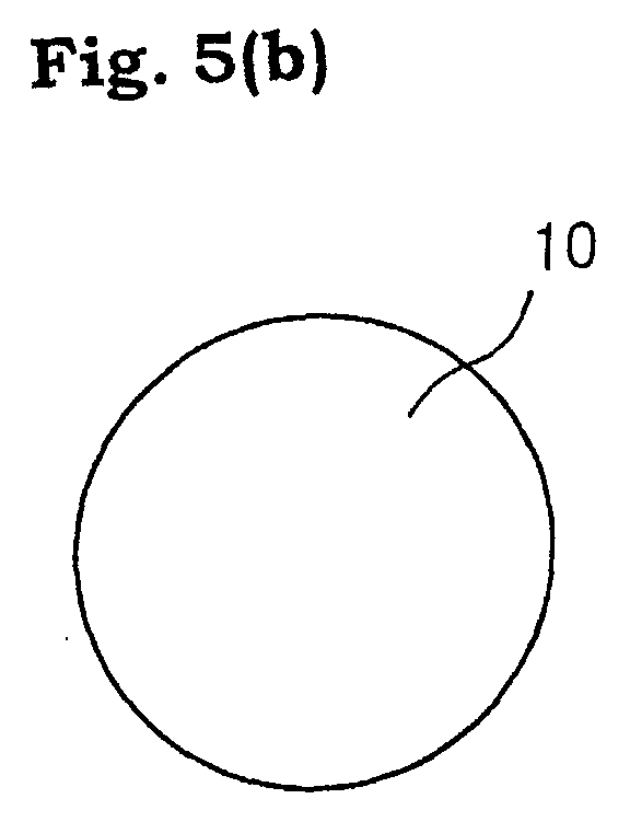
- Fig. 15(a) shows a plan view of a silicon substrate 10 of a single conductive type
- Fig. 15(b) shows an area SP (Silicon Pillar) in the silicon substrate 10 where a silicon pillar or a silicon trench having a surface oriented in a specific crystal orientation is formed.
- SP Silicon Pillar
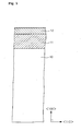
- a thermal oxide film is formed as a pad oxide film with a thickness of about 5 to 20 nm, as need arises, on the surface of the silicon substrate 10 having the surface of plane (100).
- a silicon oxide film 11 is deposited with a thickness of about 100 to 2000 nm.
- an amorphous silicon film 12 is deposited to form a hard mask (Fig. 1).
- the amorphous silicon film 12 and the silicon oxide film 11 are successively etched by reactive ion etching of a known photolithography technique using a circularly patterned resist pattern (dot pattern) 14 as a mask (Fig. 2), whereby the hard mask is circularly patterned (Fig. 3).
- the resist pattern 14 is desirably a circle in order to expose the surface of plane (100) with a shallower etching depth upon silicon etching, it may be an ellipse shape, symmetric polygon (for example, octagon, square or rectangular) or the like.
- the resist pattern 14 is removed by ashing, and then, the resulting substrate is subjected to a post-treatment with hydrogen fluoride (HF) solution.
- HF hydrogen fluoride
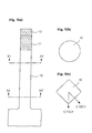
- the silicon substrate 10 is etched by the reactive ion etching using the circularly patterned hard mask as a mask, i.e., using the silicon oxide film 11 and the amorphous silicon film 12 as a mask (Fig. 4(a)).
- gases usable for anisotropically etching the silicon substrate 10 include chlorine gas (Cl 2 ), hydrogen bromide gas (HBr), oxygen gas (O 2 ) or mixture gases of these.
- the formed silicon pillar has a shape along the shape of the mask. Specifically, the formed silicon pillar becomes a circular cylinder as shown in Fig. 4(b) (Fig. 4(b) shows a section cut along the X1 - X1' line in Fig. 4(a)) when the circular mask is used.
- Each surface of the prism silicon pillar is oriented in plane (100), while each corner of the prism corresponds to the plane (110). Consequently, a silicon pillar having surfaces oriented in the specific crystal orientations is formed self-alignedly without deviation in the orientations by the above process.
- Figs. 6 to 8 is a specific embodiment wherein the silicon pillar having a surface oriented in a specific crystal orientation is used for evaluating the plane orientation dependence upon forming a thermal oxide film.
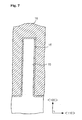
- a thermal oxide film 15 is formed (Fig. 6) on the prism silicon pillar, according to need, after removing the silicon oxide film 11 and the amorphous silicon film 12 (this embodiment shows the case where they are removed). Then, a silicon oxide film 16 is embedded at the space between pillars (Fig. 7). Thereafter, the resulting semiconductor substrate is polished from the upper surface thereof by a known chemical mechanical polishing technique (CMP), and thereby a section of the thermal oxide film 15 formed on the sidewalls of the pillars is exposed (Fig. 8(a)).
- CMP chemical mechanical polishing technique
- the side and corner of a section of the prism silicon pillar are observed from the top thereof with, for example, a scanning electron microscope (SEM).
- SEM scanning electron microscope
- one prism silicon pillar has at least four sides and corners, many samples can be obtained in a short period for evaluating the plane orientation dependence with respect to thermal oxidation of the silicon oxide film using a statistical technique. Therefore, highly reliable measuring results can be obtained.
- the plane orientation dependence with respect to the thermal oxidation may be evaluated by observing the silicon pillar in a state of a substantial prism defined by surfaces oriented in plane (100) as shown in Fig. 8(b) or by observing a columnar silicon pillar in a state of having a surface oriented in plane (100) on a portion of a side face thereof as shown in Fig. 8(c).
- the silicon pillar having the surface oriented in the specific crystal orientation by reactive ion etching may be used for a reference of a photomask alignment to accurately determine a crystallographic reference orientation of the silicon wafer, like the plane orientation reference pattern formed with the conventional isotropic etching using an alkali solution.
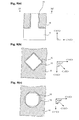
- Figs. 9(a) to 9(c) is one embodiment wherein a silicon pillar is used for a specific plane orientation reference pattern on the silicon substrate.
- two silicon pillars 10 each having a surface oriented in plane (100) are formed in such a manner that they are spaced from each other.
- the upper section of each pillar is removed by a CMP technique, as required, so that side faces of the silicon pillars 10 oriented in plane (100) can be confirmed from the top surface (Fig. 9(a)).
- a resist pattern 19 having a square window and a rectangle window which are spaced from each other like the two silicon pillars is aligned and arranged on the silicon substrate in such a manner that each side of the silicon pillars 10 is parallel to each side of the windows (Fig. 9(b)).
- the position alignment mark line of the photomask directs true direction ⁇ 100> of the silicon wafer (Fig. 9(c)).
- a element isolation region formed by shallow trench isolation method is simultaneously formed on the silicon wafer without performing isotropic etching with alkali solution, thereby reducing the number of production steps.
- a silicon trench having a surface oriented in a specific crystal orientation may be formed.
- a specific manufacturing example of the silicon trench will be explained with reference to Figs. 10 to 14.
- a thermal oxide film (not shown) is formed as a pad oxide film with a thickness of about 11 nm, as need arises, on the surface of the silicon substrate 10 having plane (100). Thereafter, a silicon oxide film 11 is deposited, and then, an amorphous silicon film 12 is deposited.
- the processes so far are the same as those of EXAMPLE 1 (Figs. 1 to 5).
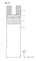
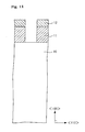
- the hard mask is etched by reactive ion etching, in the same manner as in the previous example, with a resist pattern (hole pattern) 14 having a circular opening used for a mask with respect to the silicon substrate 10 (Fig. 10).
- the resist pattern 17 is ashed and the resulting substrate is subjected to the post-treatment with fluoride hydrogen (HF) solution (Fig. 11).
- HF fluoride hydrogen
- the anisotropic etching is performed so that the depth of the silicon substrate 10 is sufficiently large with respect to the size (hole) of the mask.
- a silicon trench having the surface oriented in the specific crystal orientation is formed at a lower section of the pillar (Fig. 12(a)).
- Fig. 12(b) shows a sectional view taken along X4 - X4' line in Fig. 12(a)
- Figs. 12(c) and (d) show sectional views taken along X5 - X5' line in Fig. 12(a).
- Fig. 12(c) shows the case where the oriented surface is of plane (100)
- Fig. 12(d) shows the case where the oriented surface is of plane (110).
- the bottom surface of the trench formed with respect to the silicon substrate having a surface of plane (100) is also of plane (100). This results in all inner surfaces of the trench being of plane (100), which means all the inner surfaces of the trench are self-alignedly matched with each other to plane (100) without need to perform a special positional alignment.
- gate oxide films formed in the silicon trench have a uniform thickness with their plane orientations being matched to each other. Thereby a device with high performance in which the occurrence of the area with a reduced dielectric voltage is avoided can accurately and easily be manufactured without performing a complicated positional alignment.
- plane (100) in which the oxidation rate is the slowest can enhance controllability on forming the oxide film.
- the silicon oxide films 16 and 18 may be each formed of a single film of a polycrystalline silicon film, silicon nitride film or the like or a laminate film thereof. Any material can be used therefor if it can embed the trench or the space between the pillars.
- the silicon pillar or silicon trench having the surface oriented in the specific crystal orientation may once be sacrificially oxidized, and then, may be used after removing the formed sacrificial oxide film.
- the embodiments of the present invention represent the cases where the prism silicon pillar is used for evaluating the plane orientation and as the plane orientation reference pattern upon forming the thermal oxide film and the case where the prism silicon trench is applied for a device.
- the prism silicon pillar may be applied for a device as it is or the prism silicon trench may be used for evaluating the plane orientation and as a plane orientation reference pattern upon forming the thermal oxide film. These are only examples in which the surface oriented in the specific crystal orientation is applied to a plane orientation evaluation of silicon or to a device producing utilizing the plane orientation dependence.
- At least one or more plane orientations can simultaneously and easily be evaluated on the same wafer as well as highly precise evaluation results can be obtained, without causing a theoretical deviation.
- a trench or a pillar having plane orientations all perfectly matched with one another can easily be manufactured. Therefore, a highly reliable semiconductor device can be obtained in which a troublesome process for matching plane orientations is eliminated and deviation in the properties of a device is prevented.
- one or more plane orientations i.e., the plane orientation dependence with respect to one or more properties can accurately and easily be evaluated on a semiconductor wafer.
- a pattern for obtaining a crystallographic reference orientation can be manufactured on the semiconductor wafer having plane (100).
- a prism trench having plane orientations all matched with one another can self-alignedly be obtained when a wafer whose plane orientation dependence has been evaluated is applied for a device.
Landscapes
- Testing Or Measuring Of Semiconductors Or The Like (AREA)
- Drying Of Semiconductors (AREA)
Abstract

Description
Claims (11)
- A method for evaluating a plane orientation dependence of a semiconductor substrate comprising:forming a hard mask on a semiconductor substrate having plane orientation (100);anisotropically etching the semiconductor substrate with use of the hard mask as a mask to obtain a surface oriented in a specific crystal orientation; andevaluating a plane orientation dependence of properties of the semiconductor substrate by use of at least a portion of the surface oriented in the specific crystal orientation.
- A method claimed in Claim 1, wherein the evaluation of the plane orientation dependence is evaluation of a rate for forming a thermal oxidation film depending on the plane orientation of the semiconductor substrate.
- A method claimed in Claim 1, wherein said semiconductor substrate has a diamond crystal structure.
- A method claimed in Claim 1, wherein the surface oriented in a specific crystal orientation is of plane (100).
- A method claimed in Claim 1, wherein the hard mask is a circle or symmetric polygon.
- A method claimed in Claim 5, wherein anisotropically etching is performed to a depth of at least several times the size of the hard mask.
- A semiconductor device produced using a surface of a semiconductor substrate oriented in a specific crystal orientation as a crystallographic reference orientation, said surface being obtained by anisotropically etching a semiconductor substrate having plane orientation (100).
- A semiconductor device claimed in Claim 7, wherein the surface of the semiconductor substrate oriented in a specific crystal orientation is a surface of a pillar or a trench formed in the semiconductor substrate, and the pillar or trench is a part of the semiconductor device.
- A semiconductor device claimed in Claim 7, wherein the surface oriented in the specific crystal orientation is of plane (100).
- A method for aligning a photomask comprising:forming a hard mask on a semiconductor substrate having plane orientation (100);anisotropically etching the semiconductor substrate with use of the hard mask as a mask to obtain a pillar or trench having a surface oriented in a specific crystal orientation; andaligning a photomask using the obtained surface of the pillar or trench as a reference pattern.
- A method according to claim 10, wherein two pillars or trenches are obtained in the form of prisms each having a surface oriented in a specific crystal orientation by anisotropic etching, the two pillars or trenches being separate from each other,
the photomask has a pattern provided with two marks at a spaced interval, the two marks being in a parallel relation and each having two pairs of parallel sides, and
the photomask is aligned by putting the sides of the marks of the photomask in parallel with the sides of the pillars or trenches.
Applications Claiming Priority (2)
| Application Number | Priority Date | Filing Date | Title |
|---|---|---|---|
| JP2001190277A JP3875047B2 (en) | 2001-06-22 | 2001-06-22 | Method for evaluating plane orientation dependence of semiconductor substrate and semiconductor device using the same |
| JP2001190277 | 2001-06-22 |
Publications (2)
| Publication Number | Publication Date |
|---|---|
| EP1271642A2 true EP1271642A2 (en) | 2003-01-02 |
| EP1271642A3 EP1271642A3 (en) | 2005-09-21 |
Family
ID=19029074
Family Applications (1)
| Application Number | Title | Priority Date | Filing Date |
|---|---|---|---|
| EP02254340A Withdrawn EP1271642A3 (en) | 2001-06-22 | 2002-06-21 | Method for evaluating dependence of properties of semiconductor substrate on plane orientation and semiconductor device using the same |
Country Status (5)
| Country | Link |
|---|---|
| US (1) | US7141506B2 (en) |
| EP (1) | EP1271642A3 (en) |
| JP (1) | JP3875047B2 (en) |
| KR (1) | KR100497051B1 (en) |
| TW (1) | TW546720B (en) |
Families Citing this family (13)
| Publication number | Priority date | Publication date | Assignee | Title |
|---|---|---|---|---|
| KR100483035B1 (en) * | 2001-03-30 | 2005-04-15 | 샤프 가부시키가이샤 | A semiconductor memory and its production process |
| JP3963664B2 (en) * | 2001-06-22 | 2007-08-22 | 富士雄 舛岡 | Semiconductor memory device and manufacturing method thereof |
| EP1271652A3 (en) * | 2001-06-22 | 2004-05-06 | Fujio Masuoka | A semiconductor memory and its production process |
| US6872630B1 (en) * | 2002-06-12 | 2005-03-29 | Taiwan Semiconductor Manufacturing Company | Using V-groove etching method to reduce alignment mark asymmetric damage in integrated circuit process |
| DE10255866B4 (en) * | 2002-11-29 | 2006-11-23 | Infineon Technologies Ag | Methods and structures for increasing the pattern density and the storage capacity in a semiconductor wafer |
| US6902962B2 (en) * | 2003-04-04 | 2005-06-07 | Taiwan Semiconductor Manufacturing Company, Ltd. | Silicon-on-insulator chip with multiple crystal orientations |
| DE102004054558A1 (en) * | 2004-11-11 | 2006-05-24 | Infineon Technologies Ag | Phase change random access memory cell manufacturing method, involves back etching portion of structured hard mask by isotropic etching and back etching upper electrode layer and switching active layer by dry etching |
| JP5264383B2 (en) * | 2008-09-17 | 2013-08-14 | 東京エレクトロン株式会社 | Dry etching method |
| JP2010287739A (en) * | 2009-06-11 | 2010-12-24 | Elpida Memory Inc | Semiconductor device and manufacturing method of semiconductor device |
| JP2011103340A (en) * | 2009-11-10 | 2011-05-26 | Elpida Memory Inc | Semiconductor device, semiconductor chip, and method of manufacturing semiconductor device |
| JP2013012553A (en) | 2011-06-28 | 2013-01-17 | Toshiba Corp | Semiconductor storage device |
| US9142400B1 (en) | 2012-07-17 | 2015-09-22 | Stc.Unm | Method of making a heteroepitaxial layer on a seed area |
| WO2015125204A1 (en) * | 2014-02-18 | 2015-08-27 | ユニサンティス エレクトロニクス シンガポール プライベート リミテッド | Semiconductor device manufacturing method and semiconductor device |
Family Cites Families (30)
| Publication number | Priority date | Publication date | Assignee | Title |
|---|---|---|---|---|
| US4309813A (en) | 1979-12-26 | 1982-01-12 | Harris Corporation | Mask alignment scheme for laterally and totally dielectrically isolated integrated circuits |
| US4470875A (en) | 1983-11-09 | 1984-09-11 | At&T Bell Laboratories | Fabrication of silicon devices requiring anisotropic etching |
| JPH01287470A (en) | 1987-12-26 | 1989-11-20 | Aisin Seiki Co Ltd | Semiconductor acceleration sensor |
| JPH02230751A (en) * | 1989-03-03 | 1990-09-13 | Hitachi Ltd | Crystal orientation identification method and mechanical device created using this method |
| JPH05335197A (en) * | 1992-05-27 | 1993-12-17 | Oki Shisutetsuku Tokai:Kk | Semiconductor crystal substrate aligning method and aligning mark |
| TW248612B (en) | 1993-03-31 | 1995-06-01 | Siemens Ag | |
| JPH07283117A (en) | 1994-04-13 | 1995-10-27 | Oki Electric Ind Co Ltd | Mask alignment method |
| JP3391418B2 (en) * | 1994-04-28 | 2003-03-31 | 富士通株式会社 | Semiconductor device and manufacturing method thereof |
| JPH08236748A (en) * | 1995-02-22 | 1996-09-13 | Fujitsu Ltd | Quantum semiconductor device and manufacturing method thereof |
| JPH08130230A (en) | 1994-10-31 | 1996-05-21 | Matsushita Electric Ind Co Ltd | Flip chip mounting equipment |
| JPH08167586A (en) | 1994-12-15 | 1996-06-25 | Matsushita Electric Works Ltd | Manufacture of semiconductor device and wafer used therefor |
| US6433382B1 (en) | 1995-04-06 | 2002-08-13 | Motorola, Inc. | Split-gate vertically oriented EEPROM device and process |
| JP3315321B2 (en) | 1996-08-29 | 2002-08-19 | 株式会社東芝 | Semiconductor device and its manufacturing method, and nonvolatile semiconductor memory device and its manufacturing method |
| JP3667906B2 (en) | 1996-11-25 | 2005-07-06 | 三洋電機株式会社 | Semiconductor device and manufacturing method of semiconductor device |
| US5929477A (en) | 1997-01-22 | 1999-07-27 | International Business Machines Corporation | Self-aligned diffused source vertical transistors with stack capacitors in a 4F-square memory cell array |
| TW454339B (en) | 1997-06-20 | 2001-09-11 | Hitachi Ltd | Semiconductor integrated circuit apparatus and its fabricating method |
| JPH1154731A (en) | 1997-07-31 | 1999-02-26 | Nec Corp | Semiconductor device |
| JP3519579B2 (en) * | 1997-09-09 | 2004-04-19 | 株式会社ルネサステクノロジ | Semiconductor device and manufacturing method thereof |
| US6198114B1 (en) * | 1997-10-28 | 2001-03-06 | Stmicroelectronics, Inc. | Field effect transistor having dielectrically isolated sources and drains and method for making same |
| KR100301370B1 (en) * | 1998-04-29 | 2001-10-27 | 윤종용 | Method for manufacturing dram cell capacitor |
| US6426254B2 (en) * | 1999-06-09 | 2002-07-30 | Infineon Technologies Ag | Method for expanding trenches by an anisotropic wet etch |
| JP2001035943A (en) | 1999-07-23 | 2001-02-09 | Mitsubishi Electric Corp | Semiconductor device and manufacturing method |
| JP4350227B2 (en) | 1999-09-20 | 2009-10-21 | キヤノン株式会社 | Semiconductor crystal growth method |
| US6150670A (en) * | 1999-11-30 | 2000-11-21 | International Business Machines Corporation | Process for fabricating a uniform gate oxide of a vertical transistor |
| US6335247B1 (en) * | 2000-06-19 | 2002-01-01 | Infineon Technologies Ag | Integrated circuit vertical trench device and method of forming thereof |
| JP4226205B2 (en) | 2000-08-11 | 2009-02-18 | 富士雄 舛岡 | Manufacturing method of semiconductor memory device |
| US6387757B1 (en) | 2001-01-17 | 2002-05-14 | Taiwan Semiconductor Manufacturing Company, Ltd | Sacrificial self aligned spacer layer ion implant mask method for forming a split gate field effect transistor (FET) device |
| JP3664987B2 (en) | 2001-03-14 | 2005-06-29 | シャープ株式会社 | Electron microscope observation sample preparation method and semiconductor device analysis method |
| KR100483035B1 (en) | 2001-03-30 | 2005-04-15 | 샤프 가부시키가이샤 | A semiconductor memory and its production process |
| EP1271652A3 (en) | 2001-06-22 | 2004-05-06 | Fujio Masuoka | A semiconductor memory and its production process |
-
2001
- 2001-06-22 JP JP2001190277A patent/JP3875047B2/en not_active Expired - Fee Related
-
2002
- 2002-06-20 US US10/175,076 patent/US7141506B2/en not_active Expired - Lifetime
- 2002-06-20 KR KR10-2002-0034550A patent/KR100497051B1/en not_active Expired - Fee Related
- 2002-06-21 EP EP02254340A patent/EP1271642A3/en not_active Withdrawn
- 2002-06-21 TW TW091113645A patent/TW546720B/en not_active IP Right Cessation
Also Published As
| Publication number | Publication date |
|---|---|
| TW546720B (en) | 2003-08-11 |
| KR100497051B1 (en) | 2005-06-23 |
| JP3875047B2 (en) | 2007-01-31 |
| US7141506B2 (en) | 2006-11-28 |
| US20020197868A1 (en) | 2002-12-26 |
| EP1271642A3 (en) | 2005-09-21 |
| KR20030001270A (en) | 2003-01-06 |
| JP2003007790A (en) | 2003-01-10 |
Similar Documents
| Publication | Publication Date | Title |
|---|---|---|
| US7141506B2 (en) | Method for evaluating dependence of properties of semiconductor substrate on plane orientation and semiconductor device using the same | |
| CN101208786B (en) | Transistor with improved tip profile and method of making same | |
| US6864534B2 (en) | Semiconductor wafer | |
| JP5614877B2 (en) | Manufacturing method of semiconductor device | |
| US7005755B2 (en) | Semiconductor device and fabrication process thereof | |
| CN100440481C (en) | Semiconductor element and its manufacturing method | |
| US7291542B2 (en) | Semiconductor wafer and manufacturing method thereof | |
| JP5572924B2 (en) | Manufacturing method of semiconductor device | |
| US8389099B1 (en) | Asymmetrical wafer configurations and method for creating the same | |
| US8884406B2 (en) | Etch depth determination structure | |
| US9502244B2 (en) | Manufacturing method for forming semiconductor structure | |
| JP5568856B2 (en) | Manufacturing method of semiconductor device | |
| CN108735795B (en) | (0001) Hexagonal phase SiC wafer with surface epitaxy, UMOSFET device and manufacturing method thereof | |
| US20070207589A1 (en) | Registration mark within an overlap of dopant regions | |
| US20070075342A1 (en) | Semiconductor device with fin structure and method of manufacturing the same | |
| US7541120B2 (en) | Manufacturing method of semiconductor device | |
| JPH10199980A (en) | Method for manufacturing semiconductor device having crack prevention pattern | |
| RU215932U1 (en) | TEST ELEMENT FOR QUALITY CONTROL OF WELLS | |
| JP2017219757A (en) | Semiconductor device and manufacturing method thereof | |
| KR100495664B1 (en) | Method of forming field effec transistor having double fin structure | |
| CN101540292A (en) | Method for testing the stress of side wall of field effect transistor | |
| JP2000088686A (en) | Pedestal for semiconductor pressure sensor and its manufacture | |
| CN120630596A (en) | Overlay error control method | |
| TW202327025A (en) | Memory device and method of forming the same | |
| JPH0548098A (en) | Method for manufacturing semiconductor device |
Legal Events
| Date | Code | Title | Description |
|---|---|---|---|
| PUAI | Public reference made under article 153(3) epc to a published international application that has entered the european phase |
Free format text: ORIGINAL CODE: 0009012 |
|
| AK | Designated contracting states |
Kind code of ref document: A2 Designated state(s): AT BE CH CY DE DK ES FI FR GB GR IE IT LI LU MC NL PT SE TR |
|
| AX | Request for extension of the european patent |
Free format text: AL;LT;LV;MK;RO;SI |
|
| PUAL | Search report despatched |
Free format text: ORIGINAL CODE: 0009013 |
|
| AK | Designated contracting states |
Kind code of ref document: A3 Designated state(s): AT BE CH CY DE DK ES FI FR GB GR IE IT LI LU MC NL PT SE TR |
|
| AX | Request for extension of the european patent |
Extension state: AL LT LV MK RO SI |
|
| 17P | Request for examination filed |
Effective date: 20051214 |
|
| AKX | Designation fees paid |
Designated state(s): DE GB NL |
|
| 17Q | First examination report despatched |
Effective date: 20080812 |
|
| STAA | Information on the status of an ep patent application or granted ep patent |
Free format text: STATUS: THE APPLICATION IS DEEMED TO BE WITHDRAWN |
|
| 18D | Application deemed to be withdrawn |
Effective date: 20081223 |