EP1267599A1 - Radio wave absorber - Google Patents
Radio wave absorber Download PDFInfo
- Publication number
- EP1267599A1 EP1267599A1 EP01983820A EP01983820A EP1267599A1 EP 1267599 A1 EP1267599 A1 EP 1267599A1 EP 01983820 A EP01983820 A EP 01983820A EP 01983820 A EP01983820 A EP 01983820A EP 1267599 A1 EP1267599 A1 EP 1267599A1
- Authority
- EP
- European Patent Office
- Prior art keywords
- radio wave
- wave absorber
- magnetic layer
- absorber according
- magnetic
- Prior art date
- Legal status (The legal status is an assumption and is not a legal conclusion. Google has not performed a legal analysis and makes no representation as to the accuracy of the status listed.)
- Withdrawn
Links
Images







Classifications
-
- H—ELECTRICITY
- H01—ELECTRIC ELEMENTS
- H01F—MAGNETS; INDUCTANCES; TRANSFORMERS; SELECTION OF MATERIALS FOR THEIR MAGNETIC PROPERTIES
- H01F10/00—Thin magnetic films, e.g. of one-domain structure
-
- H—ELECTRICITY
- H05—ELECTRIC TECHNIQUES NOT OTHERWISE PROVIDED FOR
- H05K—PRINTED CIRCUITS; CASINGS OR CONSTRUCTIONAL DETAILS OF ELECTRIC APPARATUS; MANUFACTURE OF ASSEMBLAGES OF ELECTRICAL COMPONENTS
- H05K9/00—Screening of apparatus or components against electric or magnetic fields
- H05K9/0073—Shielding materials
- H05K9/0081—Electromagnetic shielding materials, e.g. EMI, RFI shielding
- H05K9/0088—Electromagnetic shielding materials, e.g. EMI, RFI shielding comprising a plurality of shielding layers; combining different shielding material structure
-
- H—ELECTRICITY
- H01—ELECTRIC ELEMENTS
- H01Q—ANTENNAS, i.e. RADIO AERIALS
- H01Q17/00—Devices for absorbing waves radiated from an antenna; Combinations of such devices with active antenna elements or systems
Definitions
- This invention relates to an impedance-matching radio wave absorber, and more specifically, to a thin-layered radio wave absorber useful for absorption of high frequency electromagnetic waves.
- Control of suppressing the useless radiation from the electronic equipment may be made by a method for making a change to circuit designs, or employing anti-useless radiation components and so on.
- use of these methods becomes more and more difficult for reasons of a demand for shorter period of product span and an increase in cost or the like.
- a method for applying an anti-useless radiation sheet or the like made up of a sheet-shaped composite soft magnetic material having a magnetic loss even for high frequency electromagnetic waves.
- a wireless LAN Local Area Network
- a superhighway automatic accounting system or like communication systems making use of high frequency radio waves have been also recently developed.
- any radio wave other than a target signal wave results in radio disturbance, so that development of a radio wave absorber has been required for smooth communication by absorption of the generated radio disturbance.
- Electromagnetic wave in the frequency band of 2.45GHz for instance, is used with various kinds of electronic equipment such as an electronic oven, a portable information terminal, a wireless LAN and a Bluetooth, and smooth communication when using these pieces of electronic equipment without mutual malfunctions is of importance.
- a loss term ⁇ " an imaginary component of a complex relative permittivity
- ⁇ " an imaginary component of a complex relative magnetic permeability of a relative magnetic permeability
- P wave absorption energy [W/m 3 ] per unit volume
- ⁇ is the angular frequency (2 ⁇ f, f: frequency of electromagnetic wave) of an electromagnetic wave
- ⁇ 0 magnetic permeability of free space
- ⁇ " is an imaginary component of a complex relative permittivity (a dielectric loss)
- E electric field strength of an electromagnetic wave applied from the outside
- ⁇ 0 magnetic permeability of free space
- ⁇ " is an imaginary component of a complex relative magnetic permeability(a magnetic loss)
- H magnetic field strength of the electromagnetic wave applied from the outside.
- ⁇ /6 wavelength of an electromagnetic wave
- the radio wave absorber for absorption of a plane wave a back face of the radio wave absorber is backed with a conductor, and absorption of the radio wave is made by a method for controlling phase of a reflected wave in an interface between the conductor and the radio wave absorber and a reflected wave in the front face of the radio wave absorber to offset the reflected waves each other.
- the wave absorber implemented by taking the above method is called an impedance-matching wave absorber.
- the impedance-matching radio wave absorber normally aims at a return loss of 20dB, which is considered to be equivalent to a value representing 99% absorption of the energy of the radio wave, in most cases.
- the impedance-matching radio wave absorber used for the high frequency band of not less than 1GHz It is necessary for the impedance-matching radio wave absorber used for the high frequency band of not less than 1GHz to have high relative magnetic permeability and high electric resistance.
- rubber ferrite for instance, has been heretofore widely used as a material of the impedance-matching radio wave absorber. Otherwise, carbonyl iron, form styrol carbon or the like has been also in use.
- a matching frequency and a matching thickness are determined once a material constant is established. A thickness of about 1cm, when using rubber ferrite or the like, is required for the electromagnetic wave in the frequency band of 2.45GHz, resulting in use of the radio wave absorber having the above thickness in the conventional technique.
- a thin film material containing Co is known as a material having high relative magnetic permeability enough to cover the high frequency band, as disclosed in Japanese Patent Application Laid-open No. 10-241938, for instance.
- Using this thin film material meets both high magnetic permeability and high electric resistance in a Co-Ni-Al-O thin film or the like by adopting a granular structure composed of two or more kinds of fine structures such as fine magnetic particles limited in particle size to about 4 to 7nm and grain boundaries of extremely thin ceramic film surrounding the fine magnetic particles.
- the thin film material in this case is formed in the shape of a thin film using a sputtering device, resulting in no application to a material of practical use as the radio wave absorber.
- a multi-layered radio wave absorber including a magnetic layer consisting of the above material is also often applied as the impedance-matching radio wave absorber.
- the structure available may be that having a dielectric layer on the front face of a magnetic layer backed with the conductor as described above and so on, for instance.
- the multi-layered wave absorber has advantages of easily managing matching of a reflected wave phase by reason that reflection is subjected to the control as impedance of an incident face nears space impedance, whereas having disadvantages of increasing the production cost. For that reason, in producing the impedance-matching radio wave absorber, there is a need for selection of a material and a structure in consideration of the above advantages and disadvantages, while difficulty has been experienced in passing decision on selection of the material and the structure.
- the present invention is provided in view of the above circumstances, and its object is to provide a thinner-layered radio wave absorber, which permits exact selection of a material and a structure and achieves high absorption performance for high frequency electromagnetic wave.
- a radio wave absorber comprising a magnetic layer having a thickness of not more than 1mm and arranged to have values of a real part ⁇ ' and an imaginary part ⁇ " of complex relative magnetic permeability satisfying the expression of ⁇ " ⁇ m ⁇ ' - n (m: real number of m>0, n: real number of n ⁇ 0)outside an impedance mismatching region, and a conductor fixedly attached to a face opposite to an electromagnetic-wave incident face of the magnetic layer.
- the above radio wave absorber even when having the magnetic layer of not more than 1mm in thickness, achieves satisfactory absorption characteristics for high frequency electromagnetic wave by adopting the structure that the conductor is fixedly attached to the face opposite to the electromagnetic-wave incident face of the magnetic layer of single-layered structure, and arranging the magnetic layer to have the values of the real part ⁇ ' and the imaginary part ⁇ " of the complex relative magnetic permeability of the magnetic layer satisfying the expression of ⁇ " ⁇ m ⁇ ' - n (m: real number of m>0, n: real number of n ⁇ 0) outside the impedance mismatching region.
- the return loss of not less than 20dB is achieved for the electromagnetic wave in the frequency band of 2.4 to 2.5GHz, for instance, on the assumption that 4 ⁇ m ⁇ 6 and n ⁇ 30, while the return loss of not less than 10dB is achieved on the assumption that 1.2 ⁇ m ⁇ 1.5 and n ⁇ 10.
- the return loss of not less than 20dB is also achieved on the assumption that 4 ⁇ m ⁇ 6 and n ⁇ 100, while the return loss of not less than 10dB is achieved on the assumption that 1.2 ⁇ m ⁇ 1.5 and n ⁇ 30.
- Using a magnetic material of fine textural structure limited in particle size to 1 to 100nm in the shape of powder, for instance, for dispersion into a polymeric material or the like permits formation of the magnetic layer.
- a radio wave absorber which comprises a radio wave absorptive layer having a thickness of not more than 1mm and adopting a multi-layered structure including a magnetic layer arranged to have values of a real part ⁇ ' and an imaginary part ⁇ " of complex relative magnetic permeability satisfying the expression of ⁇ " ⁇ m ⁇ ' - n (m: real number of m>0, n: real number of n ⁇ 0), and a conductor fixedly attached to a face opposite to an electromagnetic-wave incident face of the radio wave absorptive layer.
- the above radio wave absorber even when having the magnetic layer of not more than 1mm in thickness, achieves satisfactory absorption characteristics for high frequency electromagnetic wave by adopting the structure that the conductor is fixedly attached to the face opposite to the electromagnetic-wave incident face of the radio wave absorptive layer including the magnetic layer, and also arranging the magnetic layer to have the values of the real part ⁇ ' and the imaginary part ⁇ " of the complex magnetic permeability of the magnetic layer satisfying the expression of ⁇ " ⁇ m ⁇ '-n (m: real number of m>0, n: real number of n ⁇ 0).
- the return loss of not less than 20dB is achieved for the electromagnetic wave in the frequency band of 2.4 to 2.5GHz, for instance, on the assumption that 4 ⁇ m ⁇ 6 and n ⁇ 30, while the return loss of not less than 10 dB is achieved on the assumption that 1.2 ⁇ m ⁇ 1.5 and n ⁇ 10.
- the return loss of not less than 20dB is also achieved on the assumption that 4 ⁇ m ⁇ 6 and n ⁇ 100, while the return loss of not less than 10dB is achieved on the assumption that 1.2 ⁇ m ⁇ 1.5 and n ⁇ 30.
- the radio wave absorptive layer has a dielectric layer formed by kneading of ceramics with a polymeric material, for instance, in addition to the magnetic layer.
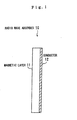
- Fig. 1 shows a structure of a radio wave absorber made up of a magnetic layer of single-layered structure.
- the radio wave absorber according to the present invention is an impedance-matching radio wave absorber having a structure that a back face of a radio wave absorptive layer made up of a magnetic layer or the like is backed with a conductor.
- the radio wave absorber of the above structure is useful for absorption of a radio wave by controlling phase of a reflected wave in an interface between the radio wave absorptive layer and the conductor and a reflected wave in a front face of the wave absorptive layer so as to offset the reflected waves each other in such a manner of allowing space impedance to match impedance of the radio wave absorptive layer by controlling the thickness of the radio wave absorptive layer.
- the radio wave absorber has an effect of absorbing a plane wave in a relatively remote electromagnetic field at a distance of not less than ⁇ /6 from a wave source.
- a radio wave absorber 10 comprising a magnetic layer 11 of single-layered structure that a face opposite to a wave incident direction of the magnetic layer 11 is backed with a metal plate as a conductor 12.
- the single-layered radio wave absorber 10 as described above has advantages of holding down its production cost, since there is less need for production steps, as compared with a multi-layered radio wave absorber which will be described later.
- the impedance-matching radio wave absorber gives effect to non-reflection in a target frequency by designing a material constant to satisfy the following expression (2), and also by controlling the thickness of the radio wave absorptive layer.
- i represents an imaginary unit
- d is the thickness of the radio wave absorber
- Fig. 2 is a graph showing relative magnetic permeability required in a case where the thickness of the magnetic layer 11 is made variable when using the single-layered radio wave absorber 10 shown in Fig.1.
- Fig. 2 there are shown values of a real part ⁇ ' and an imaginary part ⁇ " of complex relative magnetic permeability sufficient to achieve a return loss of 20dB for the electromagnetic wave in a frequency band of 2.45GHz, for instance.
- the electromagnetic wave in the frequency band of 2.45GHz is used with various kinds of electronic equipment such as an electronic oven, a portable information terminal and a wireless LAN, and is supposed to be that required for smooth communication when using these pieces of electronic equipment without mutual malfunctions.
- the relative permittivity ⁇ of the magnetic layer 11 is assumed to be 1.
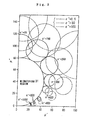
- Fig. 3 is a graph showing the relative magnetic permeability ⁇ required in a case where the relative permittivity ⁇ of the magnetic layer 11 is made variable on condition that the thickness of the magnetic layer is fixed.
- Fig. 3 there is shown a case where the relative permittivity ⁇ of the magnetic layer 11 is made variable on condition that the thickness of the magnetic layer is limited to 200 ⁇ m when using the single-layered radio wave absorber 10, similarly to Fig.2, in which inside of each circle given outside a mismatching region 31 represents values of a real part ⁇ ' and an imaginary part ⁇ " of the complex relative magnetic permeability sufficient to achieve the return loss of 20dB for the electromagnetic wave in the frequency band of 2.45GHz.
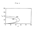
- Fig. 4 is a graph showing the relative magnetic permeability ⁇ required in a case where the thickness of the magnetic layer 11 is made variable.
- Fig. 4 there is shown how a boundary of the mismatching region insufficient to achieve the absorption of not less than -20dB varies in the case where the thickness of the magnetic layer 11 is made variable in a range from 100 to 300 ⁇ m on condition that the frequency of a target electromagnetic wave is limited to 2.45GHz when using the single-layered radio wave absorber 10 similarly.
- a semi-elliptical mismatching region having a similar shape to that shown in Fig. 3 has been obtained correspondingly to each thickness of the magnetic layer 11. It is ascertained from Fig. 4 that the smaller the thickness of the magnetic layer 11 is, the greater the mismatching region is, resulting in a need for higher relative magnetic permeability.
- Fig. 5 is a graph showing the relative magnetic permeability ⁇ required in a case where the frequency of target electromagnetic wave is made variable on condition that the thickness of the magnetic layer 11 is fixed.
- Fig. 5 there is shown how a boundary of the mismatching region insufficient to achieve the absorption characteristics of not less than -20dB varies in the case where the frequency of target electromagnetic wave is made variable in a range from 2 to 3GHz on condition that the thickness of the magnetic layer 11 is limited to 200 ⁇ m when using the single-layered radio wave absorber 10 similarly.
- a semi-elliptical mismatching region having a similar shape to that shown in Fig. 3 has been obtained correspondingly to the electromagnetic wave of each frequency. It is ascertained from Fig. 5 that the lower the frequency is, the higher will be the relative magnetic permeability required to achieve the satisfactory absorption characteristics for the target electromagnetic wave.
- the above results may formulate a guiding principle to the effect that there are needs for calculation of the mismatching region as shown in Figs.3 and 4 and also design using a material that the relative magnetic permeability is assumed to be a value outside the mismatching region in order to produce the single thin-layered radio wave absorber 10 having the magnetic layer 11 of not more than 1mm in thickness.
- Fig.6 shows a structure of a radio wave absorber made up of a radio wave absorptive layer of multi-layered structure, for instance.
- a radio wave absorber 20 shown in Fig.6 has a structure that a dielectric layer 21 consisting of a dielectric material and a magnetic layer 22 are layered as a radio wave absorptive layer on an electromagnetic wave incident face, and the radio wave absorptive layer is backed with a conductor 23.
- the radio wave absorber 20 permits a reflected wave phase to be easily matched by a reason that reflection is subjected to the control as impedance of the incident face nears space impedance in a manner of providing the magnetic layer 22 of high relative magnetic permeability on the side of the backed conductor 23 while providing the dielectric layer 21 on the electromagnetic-wave incident face side.
- the multi-layered radio wave absorber may also be of a structure having a plurality of magnetic layers or dielectric layers and so on, without being limited to the above structure.
- Fig.7 is a graph showing a relative magnetic permeability ⁇ required in a case where relative permittivity and thickness of the dielectric layer 21 are made variable when using the multi-layered radio wave absorber 20 shown in Fig. 6.
- Fig. 7 there are shown, in the shape of circles, regions of the relative magnetic permeability sufficient to achieve the absorption of not less than 20dB in a case where a real part ⁇ ' of complex relative permittivity and the thickness d2 of the dielectric layer 21 are made variable on condition that the dielectric layer 21 and the magnetic layer 22 are held to be 200 ⁇ m in total thickness, the values of the real part ⁇ ' and an imaginary part ⁇ " of the complex relative permittivity of the magnetic layer 22 are respectively assumed to be 15 and 0.5, while the values of the real part ⁇ ' and the imaginary part ⁇ " of the complex relative magnetic permeability of the dielectric layer 21 are respectively assumed to be 1 and 0 and the value of the imaginary part ⁇ " of the complex relative permittivity of the dielectric layer 21 is assumed to
- a semicircular range shown at the bottom left-hand corner is considered to be a mismatching region 71 insufficient to achieve the above absorption characteristics even though the relative magnetic permeability takes on any value within this semicircular range, and it is also ascertained that use of the magnetic layer 22 with variations in relative magnetic permeability value is possible on the outside of the mismatching region by varying the relative permittivity value and the thickness of the dielectric layer 21.
- the radio wave absorber of the present invention permits implementation of the radio wave absorber of the present invention.
- there may be two ways of implementing the wave absorber of the present invention that is, one of single-layered structure having a radio wave absorptive layer composed of only a magnetic layer and the other of multi-layered structure including a magnetic layer.
- the single-layered radio wave absorber has the advantages of holding down the production cost by reasons that there is less need for production steps as compared with the multi-layered radio wave absorber having a plurality of layers bonded together, and that control of the thickness is made easier. In this connection, examinations on what kind of requirements is required for the optimum design of the radio wave absorber will be given next.
- Fig. 8 is a graph showing most suitable requirements for selection of the materials with regard to the relative magnetic permeability of the magnetic layer.
- a semi-elliptical range shown at the bottom left-hand corner is considered to be a mismatching region 81, and when the relative magnetic permeability of the magnetic layer lies within this mismatching region, neither the single-layered radio wave absorber nor the multi-layered radio wave absorber achieves the satisfactory absorption performance.
- the region of the relative magnetic permeability sufficient to achieve the absorption characteristics of -20dB decreases with the increasing thickness of the magnetic layer.
- the above region of the relative magnetic permeability in the drawing exists within a region where the imaginary part ⁇ " of the complex relative magnetic permeability takes a value greater than a line that goes up from the origin at a certain gradient, that is, within a region satisfying the expression of ⁇ " ⁇ m ⁇ ' - n (m: real number of m>0, n: real number of n ⁇ 0).
- the values of m and n are respectively assumed to be about 5 and about 0.
- the real part ⁇ ' and the imaginary part ⁇ " of the complex relative magnetic permeability of the magnetic layer should take values meeting the requirements given by the expression of ⁇ " ⁇ m ⁇ '-n in order that the single-layered radio wave absorber may achieve the satisfactory absorption characteristics for certain frequency electromagnetic wave in the high frequency band.
- the relative magnetic permeability of the magnetic layer may basically take values in the substantially whole region except the mismatching region 81 in a manner of controlling the relative permittivity and the thickness of the dielectric layer.
- using the complex relative magnetic permeability of the magnetic layer may apply a straight line representing the expression of ⁇ " ⁇ m ⁇ ' - n (m: real number of m>0, n: real number of n ⁇ 0) as the criterion for judgment on design in order to permit production of the wave absorber sufficient to achieve the satisfactory absorption characteristics, in a region except the mismatching region 81. Accordingly, it may be judged that the region satisfying the expression of ⁇ " ⁇ m ⁇ ' - n is advantageous in producing the single-layered radio wave absorber, while the other region is advantageous in producing the multi-layered radio wave absorber. In this connection, verifications on the values of m and n in the above expression will be given next.
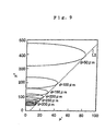
- Fig. 9 shows a matching region in a case where the relative permittivity ⁇ of the magnetic layer is assumed to be 15.
- Fig. 10 shows a matching region in a case where the relative permittivity ⁇ is assumed to be 50. Verifications on the values of m and n to meet the absorption characteristics of - 20dB with reference to Figs. 9 and 10 will be given next.
- Figs.2, 9 and 10 there are shown, every value of the relative permittivity ⁇ of the magnetic layer, matching regions sufficient to achieve the absorption characteristics of -20dB in a case where the thickness d of the magnetic layer is made variable on condition that the frequency of the target electromagnetic wave is limited to 2.45GHz.
- the value of the relative permittivity ⁇ of the magnetic layer in Fig.2 is assumed to be 1, that in Fig.9 is assumed to be 15 and that in Fig.10 is assumed to be 50.
- Figs.2, 9 and 10 there are shown the matching regions respectively corresponding to a cases where the thickness d of the magnetic layer is limited to 50 ⁇ m, 100 ⁇ m, 200 ⁇ m, 250 ⁇ m, 300 ⁇ m and more than 300 ⁇ m, as enclosed with substantially elliptical boundaries.
- the guiding principle for achievement of the return loss of not less than 20dB for the target electromagnetic wave in the frequency band of 2.4 to 2.5GHz when using the single-layered impedance-matching radio wave absorber may be set up on the basis of values of 4 ⁇ m ⁇ 6 and n ⁇ 30 when the relative permittivity ⁇ of the magnetic layer is not more than 15 on condition that the relation of the real part ⁇ ' and the imaginary part ⁇ " of the complex relative magnetic permeability of the material for the magnetic layer is given by the expression of ⁇ " ⁇ m ⁇ '- n, while being set up on the basis of values of 4 ⁇ m ⁇ 6 and n ⁇ 100 when the relative permittivity ⁇ of the magnetic layer is not more than 50.
- the value of n representing the distance from the origin gradually increases without a greater change of the value m representing the gradient, providing a greater matching region.
- Using the above guiding principle may set up the requirements for design of the thin-layered radio wave absorber, which is not more than 1mm in thickness and achieves the absorption characteristics of not less than -20dB for the useless radio wave in the frequency band of 2.45GHz required for a large number of electronic equipment such as an electronic oven, a portable information terminal and a wireless LAN.
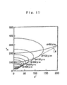
- Fig. 11 shows a matching region in a case where the relative permittivity ⁇ of the magnetic layer is assumed to be 1.
- Fig. 12 shows a matching region in the case where the relative permittivity ⁇ is assumed to be 15.
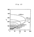
- Fig. 13 shows a matching region in the case where the relative permitivity ⁇ is assumed to be 50.
- the relative magnetic permeability ⁇ required for the magnetic layer to meet the amount of absorption of -10dB increases with the decreasing thickness d, similarly to the case of aiming at the absorption characteristics of -20dB.
- the matching regions appear on the left side of a straight line given at a certain gradient in each of Figs. 11, 12 and 13.
- the straight line as described above is shown by dotted lines as L4, L5 and L6 respectively in Figs.11, 12 and 13.
- the guiding principle for achievement of the return loss of not less than 10dB for the target electromagnetic wave in the frequency band of 2.4 to 2.5GHz when using the single-layered impedance-matching radio wave absorber may be set up on the basis of the values of 1.2 ⁇ m ⁇ 1.5 and n ⁇ 10 when the relative permittivity ⁇ of the magnetic layer is not more than 15 on condition that the relation between the real part ⁇ ' and the imaginary part ⁇ " of the complex relative magnetic permeability of the material for the magnetic layer is given by the expression of ⁇ " ⁇ m ⁇ ' - n, while being set up on the basis of the values of 1.3 ⁇ m ⁇ 1.5 and n ⁇ 30 when the relative permittivity ⁇ of the magnetic layer is not more than 50.
- the value of n gradually increases without a greater change of the value of m, providing a greater matching region.
- the matching region based on the single-layered radio wave absorber increases with the decreasing value of m, providing a greater tolerance on design.
- This embodiment aims at providing the radio wave absorber, which meets the absorption characteristics of -20dB for the electromagnetic wave in the frequency band of 2.45GHz and also the thickness of not more than 1mm.
- FeCo alloy is known as a material, which meets the above requirements.
- high magnetic permeability and high electric resistance were achieved by using the FeCo alloy and besides, by keeping up a nano-granular structure taking the shape of fine texture composed of fine magnetic particles limited in particle size to 1 to 100nm and extremely thin grain boundaries based on high resistance substance such as Al 2 O 3 or like ceramics surrounding the magnetic fine particles by precipitation or the like.
- Such a FeCo metal soft magnetic material may be used to combine with a generally available polymeric material into the shape of a sheet as the radio wave absorber.
- the above magnetic material will be prepared in the shape of powder having the nano-granular structure.
- the suitable particle size is in a range from 10 to 50nm in consideration of the need for filling to powder.
- the above powder material dispersed into a polymeric material at a volume filling rate of 30 to 60% produces a paste-like sample, which is then leveled to a predetermined thickness by a doctor blade process into the shape of a sheet.
- the polymeric material chlorinated polyethylene, rubber materials, ABS resins, and poly-lactic acid having biodegradation or the like may be used, or alternatively, thermosetting resins, photo-curing resins or the like may be used for hardening. Use may be also made of concrete, ceramics or the like, instead of the polymeric material.
- the sheet-shaped material as described above was used to produce the single-layered radio wave absorber as shown in Fig. 1, as the first embodiment.
- Use of the above material was capable of producing a sample that the real part ⁇ ' and the imaginary part ⁇ " of the complex relative magnetic permeability of the magnetic layer respectively take values of 5 and 80, resulting in achievement of the satisfactory absorption characteristics on condition that the thickness of the magnetic layer is reduced to a far smaller value as much as 200 ⁇ m than that in the conventional art.
- Fig. 14 shows the radio wave absorption characteristics in the first embodiment.
- the absorption characteristics of not less than -20dB are achieved for a TEM wave (Transverse Electric Magnetic wave) from the front face in the frequency band around 2.45GHz, providing the return loss of not less than 99%.
- TEM wave Transverse Electric Magnetic wave
- the same absorption characteristics are also achieved in a wide frequency band of about 2 to 3GHz in the first embodiment, as to the absorption characteristics of not less than -10dB, at which the effects as the radio wave absorber are to be generally accepted.
- aluminum foil was used for a backing conductor of the magnetic layer.
- a carbon film, an ITO (Indium Tin Oxide) film and other various kinds of metal films may be used without being limited to the aluminum foil. These films may be produced as a vacuum-evaporation film or a sputtering film, or alternatively, a metal face of a structure on which the radio wave absorber is installed may be made equivalent to the backing conductor.
- the radio wave absorber having the radio wave absorptive layer of a multi-layered structure having the dielectric layer and the magnetic layer as shown in Fig. 6, as the second embodiment.
- the radio wave absorber was produced by the steps of dispersing BaO-TiO 2 ceramics into a polymeric material used as a base material to form a dielectric layer as the sheet-shaped material, then pressure-bonding the dielectric layer with a magnetic layer consisting of the same material as that in the first embodiment after leveling the dielectric layer and the magnetic layer to a predetermined thickness, and then backing the magnetic layer with the aluminum foil.
- the materials other than the aluminum foil and the processes similar to those in the first embodiment will be also enough.
- the above material was capable of producing a sample that the dielectric constants of the dielectric layer and the magnetic layer respectively take values of 300 and 15 and the real part ⁇ ' and the imaginary part ⁇ " of the complex relative magnetic permeability respectively take values of 80 and 50, resulting in achievement of the absorption characteristics of not less than -20dB for the electromagnetic wave in the frequency band of 2.45GHz on condition that the thickness of the dielectric layer and that of the magnetic layer are respectively limited to 30 ⁇ m and 120 ⁇ m, in total 150 ⁇ m.
- the satisfactory absorption characteristics for the high frequency electromagnetic wave may be achieved with the thickness of not more than 1mm, while there has been need for a thickness of about not less than 1cm in the conventional art. It is extremely effective in incorporating the above radio wave absorber in the small-sized electronic equipment such as the portable information terminal, for instance, since demands for smaller size and lighter weight are satisfied.
- the radio wave absorber produced according to the above method may be applied to a radio wave absorption panel and a radio wave absorption casing, without being limited to a wave absorption sheet formed in the shape of a sheet.
- the method for producing the radio wave absorber by kneading the magnetic material with the polymeric material makes it possible to easily form the thin-layered radio wave absorber by the steps of producing a paste-like or liquid sample in a manner of controlling the volume filling rate of the magnetic material, and then coating the face of a panel-shaped body or an electronic equipment casing with the sample by spraying or the like.
- the magnetic material used for the magnetic layer either a material containing at least one of Fe, Co and Ni or an alloy containing Mn such as MmAl, CnzMnAl and MnBi may be used, without being limited to the above material.
- ceramics such as PbTiO 3 -PbZrO 3 (PZT ceramics), PbO 2 -Li 2 O 3 -ZrO 2 -TiO 2 (PLTZ ceramics), MgTiO 3 -CaTiO 3 , BaMg 1-x Ta x O 3 , BZn 1-x Ta x O 3 , Ba 2 TiO 2 , Zr 1-x Sn x TiO 4 , BaO-Nd 2 O 3 -TiO 2 , Pb 1-x Ca x ZrO 3 and PbTiO 3 -PrZrO 3 -PbB 1(1-x) B 2(x) O 3 or like ceramics may be used, without being limited to BaO-TiO 2 ceramics described the above.
- the radio wave absorber according to the present invention may achieve the satisfactory absorption characteristics for the high frequency electromagnetic wave by adopting the structure that the conductor is fixedly attached to the face opposite to the electromagnetic-wave incident face of the magnetic layer of single-layered structure, and also by arranging the magnetic layer on the assumption that the values of the real part ⁇ ' and the imaginary part ⁇ " of the complex magnetic permeability of the magnetic layer satisfy the expression of ⁇ " ⁇ m ⁇ '- n (m: real number of m>0, and n: real number of n ⁇ 0) outside the impedance mismatching region.
- the radio wave absorber according to the present invention may also achieve the satisfactory absorption characteristics for the high frequency electromagnetic wave by adopting the structure that the conductor is fixedly attached to the face opposite to the electromagnetic-wave incident face of the wave absorptive layer including the magnetic layer and also by arranging the magnetic layer on the assumption that the values of the real part ⁇ ' and the imaginary part ⁇ " of the complex magnetic permeability of the magnetic layer satisfy the expression of ⁇ " ⁇ m ⁇ ' - n (m: real number of m>0, n: real number of n ⁇ 0) outside the impedance mismatching region.
Landscapes
- Engineering & Computer Science (AREA)
- Physics & Mathematics (AREA)
- Electromagnetism (AREA)
- Microelectronics & Electronic Packaging (AREA)
- Power Engineering (AREA)
- Shielding Devices Or Components To Electric Or Magnetic Fields (AREA)
- Hard Magnetic Materials (AREA)
- Soft Magnetic Materials (AREA)
- Aerials With Secondary Devices (AREA)
- Noise Elimination (AREA)
Abstract
There is disclosed a thinner-layered radio wave absorber having high absorption performance for a high frequency electromagnetic wave. The radio wave absorber, even when having a magnetic layer of not more than 1mm in thickness, achieves satisfactory absorption characteristics for the high frequency electromagnetic wave by adopting a structure that a conductor is fixedly attached to a face opposite to an electromagnetic-wave incident face of the magnetic layer of single-layered structure, and also arranging the magnetic layer to have values of a real part mu ' and an imaginary part mu " of complex relative magnetic permeability of the magnetic layer satisfying an expression of mu ">/=m mu ' - n (m: real number of m>0, n: real number of n>/=0) outside an impedance mismatching region. <IMAGE>
Description
This invention relates to an impedance-matching
radio wave absorber, and more specifically, to a thin-layered
radio wave absorber useful for absorption of high
frequency electromagnetic waves.
Recently, with a demand for higher frequency of a
signal used with electronic equipment, a problem of
useless radiation emitted from the electronic equipment
becomes marked. Control of suppressing the useless
radiation from the electronic equipment may be made by a
method for making a change to circuit designs, or
employing anti-useless radiation components and so on.
However, use of these methods becomes more and more
difficult for reasons of a demand for shorter period of
product span and an increase in cost or the like. In
this connection, there is a tendency toward use of a
method for applying an anti-useless radiation sheet or
the like made up of a sheet-shaped composite soft
magnetic material having a magnetic loss even for high
frequency electromagnetic waves.
A wireless LAN (Local Area Network), a superhighway
automatic accounting system or like communication systems
making use of high frequency radio waves have been also
recently developed. However, in a radio wave-handling
equipment applied to these communication systems, any
radio wave other than a target signal wave results in
radio disturbance, so that development of a radio wave
absorber has been required for smooth communication by
absorption of the generated radio disturbance.
Electromagnetic wave in the frequency band of 2.45GHz,
for instance, is used with various kinds of electronic
equipment such as an electronic oven, a portable
information terminal, a wireless LAN and a Bluetooth, and
smooth communication when using these pieces of
electronic equipment without mutual malfunctions is of
importance.
While the radio wave absorber is useful to
transform energy of incident radio wave into heat for
absorption, it is supposed that a loss term ε" (an
imaginary component of a complex relative
permittivity )of a relative permittivity of the radio
wave absorber and a loss term µ" (an imaginary component
of a complex relative magnetic permeability) of a
relative magnetic permeability are related to
transformation of the energy of incident radio wave.
When incidence of a radio wave on a material having a
loss as described above occurs, the energy of the radio
wave is transformed into heat for absorption according to
the following expression (1).
P=1/2ωε0 ε" | E2 | +1/2ωµ0 µ" | H2 |
In the above expression (1), P represents wave
absorption energy [W/m3] per unit volume, ω is the
angular frequency (2πf, f: frequency of electromagnetic
wave) of an electromagnetic wave, ε0 is magnetic
permeability of free space, ε" is an imaginary component
of a complex relative permittivity (a dielectric loss), E
is electric field strength of an electromagnetic wave
applied from the outside, µ0 is magnetic permeability of
free space, µ" is an imaginary component of a complex
relative magnetic permeability(a magnetic loss), and H is
magnetic field strength of the electromagnetic wave
applied from the outside.
According to the above expression (1), the higher
loss that a material has, the greater will be the radio
wave absorptive power. However, in a case of a plane
wave in a relatively remote electromagnetic field at a
distance of not less than λ/6 (λ: wavelength of an
electromagnetic wave) from a wave source, if incidence of
a radio wave on such a high loss material just for once
is all that occurs, complete absorption of energy of the
radio wave for transformation into heat is made
impossible in most cases. This is because reflection
takes place on a front face of the radio wave absorber
for reason of a difference in impedance between air and
the radio wave absorber.
Accordingly, in the radio wave absorber for
absorption of a plane wave, a back face of the radio wave
absorber is backed with a conductor, and absorption of
the radio wave is made by a method for controlling phase
of a reflected wave in an interface between the conductor
and the radio wave absorber and a reflected wave in the
front face of the radio wave absorber to offset the
reflected waves each other. The wave absorber
implemented by taking the above method is called an
impedance-matching wave absorber. The impedance-matching
radio wave absorber normally aims at a return loss of
20dB, which is considered to be equivalent to a value
representing 99% absorption of the energy of the radio
wave, in most cases.
It is necessary for the impedance-matching radio
wave absorber used for the high frequency band of not
less than 1GHz to have high relative magnetic
permeability and high electric resistance. Conventionally,
rubber ferrite, for instance, has been heretofore widely
used as a material of the impedance-matching radio wave
absorber. Otherwise, carbonyl iron, form styrol carbon or
the like has been also in use. In the impedance-matching
radio wave absorber, a matching frequency and a matching
thickness are determined once a material constant is
established. A thickness of about 1cm, when using rubber
ferrite or the like, is required for the electromagnetic
wave in the frequency band of 2.45GHz, resulting in use
of the radio wave absorber having the above thickness in
the conventional technique. However, with the progress
of miniaturization of electronic equipment such as the
portable information terminal, for instance, there is a
need for smaller thickness of the radio wave absorber to
reduce the proportion of a radio wave absorber size to an
equipment size. In this connection, development of a
radio wave absorber, which meets demands for smaller
thickness and lighter weight while keeping up radio wave
absorption performance with the use of a material of
higher relative magnetic permeability, has been desired.
On the other hand, a thin film material containing
Co is known as a material having high relative magnetic
permeability enough to cover the high frequency band, as
disclosed in Japanese Patent Application Laid-open No.
10-241938, for instance. Using this thin film material
meets both high magnetic permeability and high electric
resistance in a Co-Ni-Al-O thin film or the like by
adopting a granular structure composed of two or more
kinds of fine structures such as fine magnetic particles
limited in particle size to about 4 to 7nm and grain
boundaries of extremely thin ceramic film surrounding the
fine magnetic particles. However, the thin film material
in this case is formed in the shape of a thin film using
a sputtering device, resulting in no application to a
material of practical use as the radio wave absorber.
A multi-layered radio wave absorber including a
magnetic layer consisting of the above material is also
often applied as the impedance-matching radio wave
absorber. The structure available may be that having a
dielectric layer on the front face of a magnetic layer
backed with the conductor as described above and so on,
for instance. As compared with a single-layered radio
wave absorber, the multi-layered wave absorber has
advantages of easily managing matching of a reflected
wave phase by reason that reflection is subjected to the
control as impedance of an incident face nears space
impedance, whereas having disadvantages of increasing the
production cost. For that reason, in producing the
impedance-matching radio wave absorber, there is a need
for selection of a material and a structure in
consideration of the above advantages and disadvantages,
while difficulty has been experienced in passing decision
on selection of the material and the structure.
The present invention is provided in view of the
above circumstances, and its object is to provide a
thinner-layered radio wave absorber, which permits exact
selection of a material and a structure and achieves high
absorption performance for high frequency electromagnetic
wave.
According to the present invention, in order to
solve the above problems, there is provided, in an
impedance-matching radio wave absorber, a radio wave
absorber comprising a magnetic layer having a thickness
of not more than 1mm and arranged to have values of a
real part µ' and an imaginary part µ" of complex relative
magnetic permeability satisfying the expression of µ"≧
mµ' - n (m: real number of m>0, n: real number of n≧
0)outside an impedance mismatching region, and a
conductor fixedly attached to a face opposite to an
electromagnetic-wave incident face of the magnetic layer.
The above radio wave absorber, even when having the
magnetic layer of not more than 1mm in thickness,
achieves satisfactory absorption characteristics for high
frequency electromagnetic wave by adopting the structure
that the conductor is fixedly attached to the face
opposite to the electromagnetic-wave incident face of the
magnetic layer of single-layered structure, and arranging
the magnetic layer to have the values of the real part µ'
and the imaginary part µ" of the complex relative
magnetic permeability of the magnetic layer satisfying
the expression of µ"≧mµ' - n (m: real number of m>0, n:
real number of n≧0) outside the impedance mismatching
region. When the relative permittivity of the magnetic
layer is not more than 15, the return loss of not less
than 20dB is achieved for the electromagnetic wave in the
frequency band of 2.4 to 2.5GHz, for instance, on the
assumption that 4≦m≦6 and n≦30, while the return loss
of not less than 10dB is achieved on the assumption that
1.2≦m≦1.5 and n≦10. When the relative permittivity of
the magnetic layer is not more than 50, the return loss
of not less than 20dB is also achieved on the assumption
that 4≦m≦6 and n≦100, while the return loss of not less
than 10dB is achieved on the assumption that 1.2≦m≦1.5
and n≦30. Using a magnetic material of fine textural
structure limited in particle size to 1 to 100nm in the
shape of powder, for instance, for dispersion into a
polymeric material or the like permits formation of the
magnetic layer.
According to the present invention, there is also
provided, in an impedance-matching radio wave absorber, a
radio wave absorber, which comprises a radio wave
absorptive layer having a thickness of not more than 1mm
and adopting a multi-layered structure including a
magnetic layer arranged to have values of a real part µ'
and an imaginary part µ" of complex relative magnetic
permeability satisfying the expression of µ"≦mµ' - n (m:
real number of m>0, n: real number of n≧0), and a
conductor fixedly attached to a face opposite to an
electromagnetic-wave incident face of the radio wave
absorptive layer.
The above radio wave absorber, even when having the
magnetic layer of not more than 1mm in thickness,
achieves satisfactory absorption characteristics for high
frequency electromagnetic wave by adopting the structure
that the conductor is fixedly attached to the face
opposite to the electromagnetic-wave incident face of the
radio wave absorptive layer including the magnetic layer,
and also arranging the magnetic layer to have the values
of the real part µ' and the imaginary part µ" of the
complex magnetic permeability of the magnetic layer
satisfying the expression of µ"≦mµ'-n (m: real number of
m>0, n: real number of n≧0). When the relative
permittivity of the magnetic layer is not more than 15,
the return loss of not less than 20dB is achieved for the
electromagnetic wave in the frequency band of 2.4 to
2.5GHz, for instance, on the assumption that 4≦m≦6 and
n≦30, while the return loss of not less than 10 dB is
achieved on the assumption that 1.2≦m≦1.5 and n≦10.
When the relative permittivity of the magnetic layer is
not more than 50, the return loss of not less than 20dB
is also achieved on the assumption that 4≦m≦6 and n≦100,
while the return loss of not less than 10dB is achieved
on the assumption that 1.2≦m≦1.5 and n≦30. Using a
magnetic material of the fine textural structure limited
in particle size to 1 to 100nm in the shape of powder,
for instance, for dispersion into a polymeric material or
the like permits formation of the magnetic layer. The
radio wave absorptive layer has a dielectric layer formed
by kneading of ceramics with a polymeric material, for
instance, in addition to the magnetic layer.
Hereinafter will be described an embodiment of the
present invention with reference to the accompanying
drawings. Fig. 1 shows a structure of a radio wave
absorber made up of a magnetic layer of single-layered
structure.
The radio wave absorber according to the present
invention is an impedance-matching radio wave absorber
having a structure that a back face of a radio wave
absorptive layer made up of a magnetic layer or the like
is backed with a conductor. The radio wave absorber of
the above structure is useful for absorption of a radio
wave by controlling phase of a reflected wave in an
interface between the radio wave absorptive layer and the
conductor and a reflected wave in a front face of the
wave absorptive layer so as to offset the reflected waves
each other in such a manner of allowing space impedance
to match impedance of the radio wave absorptive layer by
controlling the thickness of the radio wave absorptive
layer. The radio wave absorber has an effect of
absorbing a plane wave in a relatively remote
electromagnetic field at a distance of not less than λ/6
from a wave source. As one embodiment of the impedance-matching
radio wave absorber, there is shown, in Fig. 1,
a radio wave absorber 10 comprising a magnetic layer 11
of single-layered structure that a face opposite to a
wave incident direction of the magnetic layer 11 is
backed with a metal plate as a conductor 12. The single-layered
radio wave absorber 10 as described above has
advantages of holding down its production cost, since
there is less need for production steps, as compared with
a multi-layered radio wave absorber which will be
described later.
In general, the impedance-matching radio wave
absorber gives effect to non-reflection in a target
frequency by designing a material constant to satisfy the
following expression (2), and also by controlling the
thickness of the radio wave absorptive layer.

Wherein i represents an imaginary unit, and d is the
thickness of the radio wave absorber.
In this connection, there will be given of the
search for a material constant enough to satisfy the
above expression (2) in the following description. Fig. 2
is a graph showing relative magnetic permeability
required in a case where the thickness of the magnetic
layer 11 is made variable when using the single-layered
radio wave absorber 10 shown in Fig.1.
In Fig. 2, there are shown values of a real part µ'
and an imaginary part µ" of complex relative magnetic
permeability sufficient to achieve a return loss of 20dB
for the electromagnetic wave in a frequency band of
2.45GHz, for instance. The electromagnetic wave in the
frequency band of 2.45GHz is used with various kinds of
electronic equipment such as an electronic oven, a
portable information terminal and a wireless LAN, and is
supposed to be that required for smooth communication
when using these pieces of electronic equipment without
mutual malfunctions. Incidentally, the relative
permittivity ε of the magnetic layer 11 is assumed to be
1. In Fig. 2, inside of each boundary given in a semi-elliptical
shape represents a matching region meeting the
above requirements, and there are shown the matching
regions respectively corresponding to cases where a
thickness is limited to 50µm, 100µm, 150µm, 200µm, 250µm,
300µm and more than 300µm in a descending scale. It is
ascertained from Fig. 2 that the relative magnetic
permeability required for the magnetic layer 11 to meet
the amount of absorption as much as -20dB increases with
the decreasing thickness of the magnetic layer 11.
Incidentally, a description regarding a dotted line
in Fig. 2 will be given later.
Fig. 3 is a graph showing the relative magnetic
permeability µ required in a case where the relative
permittivity ε of the magnetic layer 11 is made variable
on condition that the thickness of the magnetic layer is
fixed. In Fig. 3, there is shown a case where the
relative permittivity ε of the magnetic layer 11 is made
variable on condition that the thickness of the magnetic
layer is limited to 200µm when using the single-layered
radio wave absorber 10, similarly to Fig.2, in which
inside of each circle given outside a mismatching region
31 represents values of a real part µ' and an imaginary
part µ" of the complex relative magnetic permeability
sufficient to achieve the return loss of 20dB for the
electromagnetic wave in the frequency band of 2.45GHz.
The circles representing the regions meeting the above
requirements are shown by solid lines, broken lines and
dotted lines respectively corresponding to cases where ε"
= 0.5, 50 and 100 on condition that the value of the real
part ε' of the complex relative permittivity is varied in
a range from 15 to 1000 and value of the imaginary part
ε" thereof is further varied depending on each value of
the real part.
As a result of measurement, inside of the
mismatching region 31 given in a semicircular shape in
Fig.3 is considered to be a region insufficient to
achieve the absorption characteristics of not less than -
20dB although the relative permittivity ε is limited to
any value. Thus, even if a material that takes the values
of the real part µ' and the imaginary part µ" of the
complex relative magnetic permeability included in the
mismatching region 31 is used, no satisfactory radio wave
absorber meeting the above requirements is available. It
is also understood that a value of the required relative
magnetic permeability decreases with the increasing
relative permittivity dielectric constant for achievement
of the above absorption characteristics. It is
ascertained from Fig.3, for instance, that supposing that
a magnetic material of about 300 in relative permittivity
is used as the magnetic layer 11, the complex relative
magnetic permeability of about µ= 60-40j is all that is
required to produce the thin-layered radio wave absorber
of 200µm in thickness.
From a standpoint that use of the magnetic material
showing the relative magnetic permeability within the
above mismatching region is beyond a range of possibility
of producing a satisfactory radio wave absorber in the
present invention, examinations on a boundary of the
mismatching region will be given next. Fig. 4 is a graph
showing the relative magnetic permeability µ required in
a case where the thickness of the magnetic layer 11 is
made variable.
In Fig. 4, there is shown how a boundary of the
mismatching region insufficient to achieve the absorption
of not less than -20dB varies in the case where the
thickness of the magnetic layer 11 is made variable in a
range from 100 to 300µm on condition that the frequency
of a target electromagnetic wave is limited to 2.45GHz
when using the single-layered radio wave absorber 10
similarly. As a result, a semi-elliptical mismatching
region having a similar shape to that shown in Fig. 3 has
been obtained correspondingly to each thickness of the
magnetic layer 11. It is ascertained from Fig. 4 that
the smaller the thickness of the magnetic layer 11 is,
the greater the mismatching region is, resulting in a
need for higher relative magnetic permeability.
Fig. 5 is a graph showing the relative magnetic
permeability µrequired in a case where the frequency of
target electromagnetic wave is made variable on condition
that the thickness of the magnetic layer 11 is fixed. In
Fig. 5, there is shown how a boundary of the mismatching
region insufficient to achieve the absorption
characteristics of not less than -20dB varies in the case
where the frequency of target electromagnetic wave is
made variable in a range from 2 to 3GHz on condition that
the thickness of the magnetic layer 11 is limited to
200µm when using the single-layered radio wave absorber
10 similarly. As a result, a semi-elliptical mismatching
region having a similar shape to that shown in Fig. 3 has
been obtained correspondingly to the electromagnetic wave
of each frequency. It is ascertained from Fig. 5 that
the lower the frequency is, the higher will be the
relative magnetic permeability required to achieve the
satisfactory absorption characteristics for the target
electromagnetic wave.
The above results may formulate a guiding principle
to the effect that there are needs for calculation of the
mismatching region as shown in Figs.3 and 4 and also
design using a material that the relative magnetic
permeability is assumed to be a value outside the
mismatching region in order to produce the single thin-layered
radio wave absorber 10 having the magnetic layer
11 of not more than 1mm in thickness.
Examinations on a radio wave absorber having a wave
absorptive layer of multi-layered structure including the
magnetic layer as one embodiment of the thin-layered
radio wave absorber having the above absorption
performance will be given next. Fig.6 shows a structure
of a radio wave absorber made up of a radio wave
absorptive layer of multi-layered structure, for instance.
A radio wave absorber 20 shown in Fig.6 has a
structure that a dielectric layer 21 consisting of a
dielectric material and a magnetic layer 22 are layered
as a radio wave absorptive layer on an electromagnetic
wave incident face, and the radio wave absorptive layer
is backed with a conductor 23. The radio wave absorber
20 permits a reflected wave phase to be easily matched by
a reason that reflection is subjected to the control as
impedance of the incident face nears space impedance in a
manner of providing the magnetic layer 22 of high
relative magnetic permeability on the side of the backed
conductor 23 while providing the dielectric layer 21 on
the electromagnetic-wave incident face side.
Incidentally, the multi-layered radio wave absorber may
also be of a structure having a plurality of magnetic
layers or dielectric layers and so on, without being
limited to the above structure.
Fig.7 is a graph showing a relative magnetic
permeability µ required in a case where relative
permittivity and thickness of the dielectric layer 21 are
made variable when using the multi-layered radio wave
absorber 20 shown in Fig. 6. In Fig. 7, there are shown,
in the shape of circles, regions of the relative magnetic
permeability sufficient to achieve the absorption of not
less than 20dB in a case where a real part ε' of complex
relative permittivity and the thickness d2 of the
dielectric layer 21 are made variable on condition that
the dielectric layer 21 and the magnetic layer 22 are
held to be 200µm in total thickness, the values of the
real part ε' and an imaginary part ε" of the complex
relative permittivity of the magnetic layer 22 are
respectively assumed to be 15 and 0.5, while the values
of the real part µ' and the imaginary part µ" of the
complex relative magnetic permeability of the dielectric
layer 21 are respectively assumed to be 1 and 0 and the
value of the imaginary part ε" of the complex relative
permittivity of the dielectric layer 21 is assumed to be
0 when using the radio wave absorber 20. Referring to
Fig.7, a semicircular range shown at the bottom left-hand
corner is considered to be a mismatching region 71
insufficient to achieve the above absorption
characteristics even though the relative magnetic
permeability takes on any value within this semicircular
range, and it is also ascertained that use of the
magnetic layer 22 with variations in relative magnetic
permeability value is possible on the outside of the
mismatching region by varying the relative permittivity
value and the thickness of the dielectric layer 21.
Selecting the material fit for use on the basis of
the above result of examinations permits implementation
of the radio wave absorber of the present invention. As
described the above, there may be two ways of
implementing the wave absorber of the present invention,
that is, one of single-layered structure having a radio
wave absorptive layer composed of only a magnetic layer
and the other of multi-layered structure including a
magnetic layer. The single-layered radio wave absorber
has the advantages of holding down the production cost by
reasons that there is less need for production steps as
compared with the multi-layered radio wave absorber
having a plurality of layers bonded together, and that
control of the thickness is made easier. In this
connection, examinations on what kind of requirements is
required for the optimum design of the radio wave
absorber will be given next.
Fig. 8 is a graph showing most suitable requirements
for selection of the materials with regard to the
relative magnetic permeability of the magnetic layer. In
Fig. 8, there is shown a region sufficient to achieve the
absorption of not less than -20dB when a frequency of the
target electromagnetic wave is limited to 2.45GHz, and
thickness of the radio wave absorptive layer is also
limited to not more than 200µm. A semi-elliptical range
shown at the bottom left-hand corner is considered to be
a mismatching region 81, and when the relative magnetic
permeability of the magnetic layer lies within this
mismatching region, neither the single-layered radio wave
absorber nor the multi-layered radio wave absorber
achieves the satisfactory absorption performance.
Referring to Fig. 2, when using the single-layered
radio wave absorber, the region of the relative magnetic
permeability sufficient to achieve the absorption
characteristics of -20dB decreases with the increasing
thickness of the magnetic layer. However, the above
region of the relative magnetic permeability in the
drawing exists within a region where the imaginary part
µ" of the complex relative magnetic permeability takes a
value greater than a line that goes up from the origin at
a certain gradient, that is, within a region satisfying
the expression of µ"≧mµ' - n (m: real number of m>0, n:
real number of n ≧0). When meeting the requirements in
Fig. 2, the values of m and n are respectively assumed to
be about 5 and about 0. Thus, the real part µ' and the
imaginary partµ" of the complex relative magnetic
permeability of the magnetic layer should take values
meeting the requirements given by the expression of µ"≧
mµ'-n in order that the single-layered radio wave
absorber may achieve the satisfactory absorption
characteristics for certain frequency electromagnetic
wave in the high frequency band. On the other hand,
referring to Fig. 7, when using the multi-layered radio
wave absorber, the relative magnetic permeability of the
magnetic layer may basically take values in the
substantially whole region except the mismatching region
81 in a manner of controlling the relative permittivity
and the thickness of the dielectric layer.
As described the above, as shown in Fig. 8, using
the complex relative magnetic permeability of the
magnetic layer may apply a straight line representing the
expression of µ"≧mµ' - n (m: real number of m>0, n: real
number of n≧0) as the criterion for judgment on design
in order to permit production of the wave absorber
sufficient to achieve the satisfactory absorption
characteristics, in a region except the mismatching
region 81. Accordingly, it may be judged that the region
satisfying the expression of µ"≧mµ' - n is advantageous
in producing the single-layered radio wave absorber,
while the other region is advantageous in producing the
multi-layered radio wave absorber. In this connection,
verifications on the values of m and n in the above
expression will be given next.
Firstly, a description will be given of
verifications on a guiding principle on selection of a
material for the magnetic layer to achieve the absorption
characteristics of -20dB when using the single-layered
radio wave absorber. Fig. 9 shows a matching region in a
case where the relative permittivity ε of the magnetic
layer is assumed to be 15. Fig. 10 shows a matching
region in a case where the relative permittivity ε is
assumed to be 50. Verifications on the values of m and n
to meet the absorption characteristics of - 20dB with
reference to Figs. 9 and 10 will be given next.
In Figs.2, 9 and 10, there are shown, every value of
the relative permittivity εof the magnetic layer,
matching regions sufficient to achieve the absorption
characteristics of -20dB in a case where the thickness d
of the magnetic layer is made variable on condition that
the frequency of the target electromagnetic wave is
limited to 2.45GHz. The value of the relative
permittivity ε of the magnetic layer in Fig.2 is assumed
to be 1, that in Fig.9 is assumed to be 15 and that in
Fig.10 is assumed to be 50. In each of Figs.2, 9 and 10,
there are shown the matching regions respectively
corresponding to a cases where the thickness d of the
magnetic layer is limited to 50µm, 100µm, 200µm, 250µm,
300µm and more than 300 µm, as enclosed with
substantially elliptical boundaries.
In Figs. 9 and 10, the relative magnetic
permeability εrequired for the magnetic layer to meet the
amount of absorption of -20dB increases with the
decreasing thickness d, similarly to the case of Fig. 2.
The matching regions appear on the left side of a
straight line given at a certain gradient in each of Figs.
9 and 10. The straight line as described above is shown
by dotted lines as L1, L2 and L3 respectively in Figs.2,
9 and 10. Expressing each of the straight lines L1, L2
and L3 in terms of µ"=mµ'- n gives m=5 and n=0 from Fig.
2 when the relative permittivity ε is 1, gives m=4.3 and
n=25 from Fig. 9 when the relative permittivity ε is 15,
and gives m=5.1 and n=75 from Fig. 10 when the relative
permittivity εis 50.
According to the above results, the guiding
principle for achievement of the return loss of not less
than 20dB for the target electromagnetic wave in the
frequency band of 2.4 to 2.5GHz when using the single-layered
impedance-matching radio wave absorber may be set
up on the basis of values of 4≦m≦6 and n≦30 when the
relative permittivity εof the magnetic layer is not more
than 15 on condition that the relation of the real part
µ' and the imaginary part µ" of the complex relative
magnetic permeability of the material for the magnetic
layer is given by the expression of µ"≧mµ'- n, while
being set up on the basis of values of 4≦m≦6 and n≦100
when the relative permittivity εof the magnetic layer is
not more than 50. As described above, with the
increased value of the relative permittivity ε of the
magnetic layer, the value of n representing the distance
from the origin gradually increases without a greater
change of the value m representing the gradient,
providing a greater matching region. Using the above
guiding principle may set up the requirements for design
of the thin-layered radio wave absorber, which is not
more than 1mm in thickness and achieves the absorption
characteristics of not less than -20dB for the useless
radio wave in the frequency band of 2.45GHz required for
a large number of electronic equipment such as an
electronic oven, a portable information terminal and a
wireless LAN.
From the standpoint that effects as the radio wave
absorber are accepted so long as not less than -10dB is
achieved, verifications on the guiding principle on
selection of the material for the magnetic layer to
achieve the absorption characteristics of not less than-10dB
will be given next. Fig. 11 shows a matching region
in a case where the relative permittivity ε of the
magnetic layer is assumed to be 1. Fig. 12 shows a
matching region in the case where the relative
permittivity ε is assumed to be 15. Fig. 13 shows a
matching region in the case where the relative
permitivity ε is assumed to be 50. A description will
now be given of verifications on the values of m and n to
meet the absorption characteristics of -10dB with
reference to Figs.11, 12 and 13.
Referring to Figs.11, 12 and 13, the relative
magnetic permeability µ required for the magnetic layer
to meet the amount of absorption of -10dB increases with
the decreasing thickness d, similarly to the case of
aiming at the absorption characteristics of -20dB. The
matching regions appear on the left side of a straight
line given at a certain gradient in each of Figs. 11, 12
and 13. The straight line as described above is shown by
dotted lines as L4, L5 and L6 respectively in Figs.11, 12
and 13. Expressing each of the straight lines L4, L5 and
L6 in terms of µ"=mµ' - n gives m=1.4 and n=0 from Fig.
11 when the relative permittivity ε is 1, gives m=1.3 and
n=5 from Fig. 12 when the relative permittivity εis 15,
and gives m=1.4 and n=25 from Fig.13 when the relative
permittivity ε is 50.
According to the above results, the guiding
principle for achievement of the return loss of not less
than 10dB for the target electromagnetic wave in the
frequency band of 2.4 to 2.5GHz when using the single-layered
impedance-matching radio wave absorber may be set
up on the basis of the values of 1.2≦m≦1.5 and n≦10
when the relative permittivity εof the magnetic layer is
not more than 15 on condition that the relation between
the real part µ' and the imaginary part µ" of the complex
relative magnetic permeability of the material for the
magnetic layer is given by the expression of µ"≧mµ' - n,
while being set up on the basis of the values of 1.3≦m≦
1.5 and n≦30 when the relative permittivity ε of the
magnetic layer is not more than 50. As described above,
with the increasing value of the relative permittivity ε
of the magnetic layer, the value of n gradually increases
without a greater change of the value of m, providing a
greater matching region. When there is a need for design
in case of reducing the target absorption characteristics
to a lower level like -10dB, the matching region based on
the single-layered radio wave absorber increases with the
decreasing value of m, providing a greater tolerance on
design.
A description will now be given of an embodiment of
the wave absorber implemented on the basis of the above
requirements for design. This embodiment aims at
providing the radio wave absorber, which meets the
absorption characteristics of -20dB for the
electromagnetic wave in the frequency band of 2.45GHz and
also the thickness of not more than 1mm.
First of all, it is necessary for a material fit for
the magnetic layer to have high relative magnetic
permeability enough to cover the high frequency band. In
general, high saturated-magnetic flux density is required
to achieve high magnetic permeability, and in this
connection, FeCo alloy is known as a material, which
meets the above requirements. In the present invention,
high magnetic permeability and high electric resistance
were achieved by using the FeCo alloy and besides, by
keeping up a nano-granular structure taking the shape of
fine texture composed of fine magnetic particles limited
in particle size to 1 to 100nm and extremely thin grain
boundaries based on high resistance substance such as
Al2O3 or like ceramics surrounding the magnetic fine
particles by precipitation or the like.
Such a FeCo metal soft magnetic material may be used
to combine with a generally available polymeric material
into the shape of a sheet as the radio wave absorber.
When using this means, the above magnetic material will
be prepared in the shape of powder having the nano-granular
structure. The suitable particle size is in a
range from 10 to 50nm in consideration of the need for
filling to powder. The thickness of the grain boundaries
is preferably limited to not more than a skin depth,
which is assumed to be about 1µm, so that the grain
boundaries of about 0.1 to 3µm in thickness are required.
That is, in terms of aspect ratio, the powder material is
assumed to be in a range from 50/0.1 = 500 at a maximum
to 3/10 = about 0.3 at a minimum. Using three pieces of
rolls to knead the above powder material dispersed into a
polymeric material at a volume filling rate of 30 to 60%
produces a paste-like sample, which is then leveled to a
predetermined thickness by a doctor blade process into
the shape of a sheet. As the polymeric material,
chlorinated polyethylene, rubber materials, ABS resins,
and poly-lactic acid having biodegradation or the like
may be used, or alternatively, thermosetting resins,
photo-curing resins or the like may be used for hardening.
Use may be also made of concrete, ceramics or the like,
instead of the polymeric material.
The sheet-shaped material as described above was
used to produce the single-layered radio wave absorber as
shown in Fig. 1, as the first embodiment. Use of the
above material was capable of producing a sample that the
real part µ' and the imaginary part µ" of the complex
relative magnetic permeability of the magnetic layer
respectively take values of 5 and 80, resulting in
achievement of the satisfactory absorption
characteristics on condition that the thickness of the
magnetic layer is reduced to a far smaller value as much
as 200µm than that in the conventional art. Fig. 14
shows the radio wave absorption characteristics in the
first embodiment.
As shown in Fig. 14, in the first embodiment, the
absorption characteristics of not less than -20dB are
achieved for a TEM wave (Transverse Electric Magnetic
wave) from the front face in the frequency band around
2.45GHz, providing the return loss of not less than 99%.
Thus, effective elimination of useless radio wave is
possible in the frequency band required for the large
number of electronic equipment such as the electronic
oven, the portable information terminal and the wireless
LAN. The same absorption characteristics are also
achieved in a wide frequency band of about 2 to 3GHz in
the first embodiment, as to the absorption
characteristics of not less than -10dB, at which the
effects as the radio wave absorber are to be generally
accepted. Incidentally, aluminum foil was used for a
backing conductor of the magnetic layer. As the backing
conductor, a carbon film, an ITO (Indium Tin Oxide) film
and other various kinds of metal films may be used
without being limited to the aluminum foil. These films
may be produced as a vacuum-evaporation film or a
sputtering film, or alternatively, a metal face of a
structure on which the radio wave absorber is installed
may be made equivalent to the backing conductor.
Then, the above material was used to produce the
radio wave absorber having the radio wave absorptive
layer of a multi-layered structure having the dielectric
layer and the magnetic layer as shown in Fig. 6, as the
second embodiment. In the second embodiment, the radio
wave absorber was produced by the steps of dispersing
BaO-TiO2 ceramics into a polymeric material used as a
base material to form a dielectric layer as the sheet-shaped
material, then pressure-bonding the dielectric
layer with a magnetic layer consisting of the same
material as that in the first embodiment after leveling
the dielectric layer and the magnetic layer to a
predetermined thickness, and then backing the magnetic
layer with the aluminum foil. As the backed conductor,
the materials other than the aluminum foil and the
processes similar to those in the first embodiment will
be also enough. Use of the above material was capable of
producing a sample that the dielectric constants of the
dielectric layer and the magnetic layer respectively take
values of 300 and 15 and the real part µ' and the
imaginary part µ" of the complex relative magnetic
permeability respectively take values of 80 and 50,
resulting in achievement of the absorption
characteristics of not less than -20dB for the
electromagnetic wave in the frequency band of 2.45GHz on
condition that the thickness of the dielectric layer and
that of the magnetic layer are respectively limited to
30µm and 120µm, in total 150µm.
In the above radio wave absorber, the satisfactory
absorption characteristics for the high frequency
electromagnetic wave may be achieved with the thickness
of not more than 1mm, while there has been need for a
thickness of about not less than 1cm in the conventional
art. It is extremely effective in incorporating the
above radio wave absorber in the small-sized electronic
equipment such as the portable information terminal, for
instance, since demands for smaller size and lighter
weight are satisfied. The radio wave absorber produced
according to the above method may be applied to a radio
wave absorption panel and a radio wave absorption casing,
without being limited to a wave absorption sheet formed
in the shape of a sheet. The method for producing the
radio wave absorber by kneading the magnetic material
with the polymeric material makes it possible to easily
form the thin-layered radio wave absorber by the steps of
producing a paste-like or liquid sample in a manner of
controlling the volume filling rate of the magnetic
material, and then coating the face of a panel-shaped
body or an electronic equipment casing with the sample by
spraying or the like.
Incidentally, as the magnetic material used for the
magnetic layer, either a material containing at least one
of Fe, Co and Ni or an alloy containing Mn such as MmAl,
CnzMnAl and MnBi may be used, without being limited to
the above material. As the dielectric material used for
the dielectric layer, ceramics such as PbTiO3-PbZrO3 (PZT
ceramics), PbO2-Li2O3-ZrO2-TiO2 (PLTZ ceramics), MgTiO3-CaTiO3,
BaMg1-xTaxO3, BZn1-xTaxO3, Ba2TiO2, Zr1-xSnxTiO4, BaO-Nd2O3-TiO2,
Pb1-xCaxZrO3 and PbTiO3-PrZrO3-PbB1(1-x)B2(x)O3 or
like ceramics may be used, without being limited to BaO-TiO2
ceramics described the above.
As has been described in the foregoing, the radio
wave absorber according to the present invention, even
when having the magnetic layer of not more than 1mm in
thickness, may achieve the satisfactory absorption
characteristics for the high frequency electromagnetic
wave by adopting the structure that the conductor is
fixedly attached to the face opposite to the
electromagnetic-wave incident face of the magnetic layer
of single-layered structure, and also by arranging the
magnetic layer on the assumption that the values of the
real part µ' and the imaginary part µ" of the complex
magnetic permeability of the magnetic layer satisfy the
expression of µ"≧mµ'- n (m: real number of m>0, and n:
real number of n≧0) outside the impedance mismatching
region.
The radio wave absorber according to the present
invention, even when having the magnetic layer of not
more than 1mm in thickness, may also achieve the
satisfactory absorption characteristics for the high
frequency electromagnetic wave by adopting the structure
that the conductor is fixedly attached to the face
opposite to the electromagnetic-wave incident face of the
wave absorptive layer including the magnetic layer and
also by arranging the magnetic layer on the assumption
that the values of the real part µ' and the imaginary
part µ" of the complex magnetic permeability of the
magnetic layer satisfy the expression of µ"≦mµ' - n (m:
real number of m>0, n: real number of n≧0) outside the
impedance mismatching region.
Claims (21)
- In an impedance-matching radio wave absorber, a radio wave absorber comprising a magnetic layer having a thickness of not more than 1mm and arranged to have values of a real part µ' and an imaginary part µ" of complex relative magnetic permeability satisfying an expression of µ" ≧ mµ' - n (m: real number of m>0, n: real number of n≧0) outside an impedance mismatching region, and a conductor fixedly attached to a face opposite to an electromagnetic-wave incident face of said magnetic layer.
- A radio wave absorber according to claim 1, wherein 4≦m≦6 and n≦30 are required, when a return loss of not less than 20dB is achieved for said electromagnetic wave in a frequency band of 2.4 to 2.5GHz on condition that the relative permittivity of said magnetic layer is not more than 15.
- A radio wave absorber according to claim 1, wherein 4≦m≦6 and n≦100 are required, when a return loss of not less than 20dB is achieved for said electromagnetic wave in a frequency band of 2.4 to 2.5GHz on condition that relative permittivity of said magnetic layer is not more than 50.
- A radio wave absorber according to claim 1, wherein 1.2≦m≦1.5 and n≦10 are required, when a return loss of not less than 10dB is achieved for said electromagnetic wave in a frequency band of 2.4 to 2.5GHz on condition that relative permittivity of said magnetic layer is not more than 15.
- A radio wave absorber according to claim 1, wherein 1.3≦m≦1.5 and n≦30 are required, when the a return loss of not less than 10dB is achieved for said electromagnetic wave in a frequency band of 2.4 to 2.5GHz on condition that relative permittivity of said magnetic layer is not more than 50.
- A radio wave absorber according to claim 1, wherein said magnetic layer contains a magnetic material having a fine textural structure limited in a particle size in a range of 1 to 100nm.
- A radio wave absorber according to claim 6, wherein said magnetic material includes either a material containing at least one of Fe, Co and Ni or an alloy containing Mn.
- A radio wave absorber according to claim 6, wherein said magnetic layer is formed by dispersion of said magnetic material in a shape of powder into any of a polymeric material, concrete and ceramics.
- In an impedance-matching radio wave absorber, a radio wave absorber comprising a radio wave absorptive layer having a thickness of not more than 1mm and adopting a multi-layered structure including a magnetic layer arranged to have values of a real part µ' and an imaginary part µ" of complex relative magnetic permeability satisfying an expression of µ"≦mµ'-n (m: real number of m>0, n: real number of n≧0) outside an impedance mismatching region, and a conductor fixedly attached to a face opposite to an electromagnetic-wave incident face of said radio wave absorptive layer.
- A radio wave absorber according to claim 9, wherein 4≦m≦6 and n≦30 are required, when a return loss of not less than 20dB is achieved for said electromagnetic wave in a frequency band of 2.4 to 2.5GHz on condition that relative permittivity of said magnetic layer is not more than 15.
- A radio wave absorber according to claim 9, wherein 4≦m≦6 and n≦100 are required, when return loss of not less than 20dB is achieved for said electromagnetic wave in a frequency band of 2.4 to 2.5GHz on condition that relative permittivity of said magnetic layer is not more than 50.
- A radio wave absorber according to claim 9, wherein 1.2≦m≦1.5 and n≦10 are required, when a return loss of not less than 10dB is achieved for said electromagnetic wave in a frequency band of 2.4 to 2.5GHz on condition that relative permittivity of said magnetic layer is not more than 15.
- A radio wave absorber according to claim 9, wherein 1.3≦m≦1.5 and n≦30 are required, when a return loss of not less than 10dB is achieved for said electromagnetic wave in the frequency band of 2.4 to 2.5GHz on condition that relative permittivity of said magnetic layer is not more than 50.
- A radio wave absorber according to claim 9, wherein said magnetic layer contains a magnetic material having a fine textural structure limited in a particle size in a range of 1 to 100nm.
- A radio wave absorber according to claim 14, wherein said magnetic material includes either a material containing at least one of Fe, Co and Ni or an alloy containing Mn.
- A radio wave absorber according to claim 14, wherein said magnetic material is formed by dispersion of said magnetic material in a shape of powder into any of a polymeric material, concrete and ceramics.
- A radio wave absorber according to claim 9, wherein said radio wave absorptive layer has a dielectric layer containing a dielectric material.
- A radio wave absorber according to claim 17, wherein said dielectric layer is formed by kneading of said dielectric material such as ceramics selected from a group consisting of BaO-TiO2, PZT, PLTZ, MgTiO3-CaTiO3, BaMg1-xTaxO3, BZn1-x TaxO3, Ba2TiO2, Zr1-xSnx TiO4, BaO-Nd2O3-TiO2, Pb1-xCaxZrO3 and PbTiO3 -PrZrO3-PbB1(1-x)B2(x)O3 ceramics with a polymeric material.
- A radio wave absorption sheet, comprising the radio wave absorber according to one of claim 1 and claim 9.
- A radio wave absorption panel, comprising the radio wave absorber according to one of claim 1 and claim 9.
- A radio wave absorption casing, comprising the radio wave absorber according to one of claim 1 and claim 9.
Applications Claiming Priority (3)
| Application Number | Priority Date | Filing Date | Title |
|---|---|---|---|
| JP2000354253 | 2000-11-21 | ||
| JP2000354253A JP2002158483A (en) | 2000-11-21 | 2000-11-21 | Radio wave absorber |
| PCT/JP2001/010112 WO2002043460A1 (en) | 2000-11-21 | 2001-11-20 | Radio wave absorber |
Publications (1)
| Publication Number | Publication Date |
|---|---|
| EP1267599A1 true EP1267599A1 (en) | 2002-12-18 |
Family
ID=18826882
Family Applications (1)
| Application Number | Title | Priority Date | Filing Date |
|---|---|---|---|
| EP01983820A Withdrawn EP1267599A1 (en) | 2000-11-21 | 2001-11-20 | Radio wave absorber |
Country Status (5)
| Country | Link |
|---|---|
| US (1) | US6670546B2 (en) |
| EP (1) | EP1267599A1 (en) |
| JP (1) | JP2002158483A (en) |
| KR (1) | KR20030007398A (en) |
| WO (1) | WO2002043460A1 (en) |
Cited By (1)
| Publication number | Priority date | Publication date | Assignee | Title |
|---|---|---|---|---|
| EP1585148A4 (en) * | 2002-12-27 | 2008-04-02 | Tdk Corp | Granular substance, magnetic thin film, and magnetic device |
Families Citing this family (15)
| Publication number | Priority date | Publication date | Assignee | Title |
|---|---|---|---|---|
| JP3838815B2 (en) * | 1999-05-10 | 2006-10-25 | 日本電気株式会社 | Mobile phone |
| JP2003283242A (en) * | 2002-03-25 | 2003-10-03 | Murata Mfg Co Ltd | Radio wave reflector and structure having the reflector mounted thereon |
| WO2003107729A1 (en) * | 2002-06-14 | 2003-12-24 | Laird Technologies, Inc. | Composite emi shield |
| TWI287065B (en) * | 2003-09-12 | 2007-09-21 | Nippon Steel Corp | Magnetic shield panel |
| JP2006186725A (en) * | 2004-12-28 | 2006-07-13 | Central Glass Co Ltd | Electromagnetic wave absorbing board |
| US7688246B2 (en) * | 2005-05-10 | 2010-03-30 | Fuji Xerox Co., Ltd. | Radio wave absorber, electromagnetic field measurement system and radiated immunity system |
| US20070046408A1 (en) * | 2005-08-30 | 2007-03-01 | Youngtack Shim | Magnet-shunted systems and methods |
| KR100835658B1 (en) * | 2006-09-05 | 2008-06-09 | 최재철 | Electromagnetic wave absorber and construction method |
| DE112008002537T5 (en) * | 2007-09-20 | 2010-07-15 | Nitto Denko Corp., Ibaraki | Electromagnetic radiation absorber and method of absorbing electromagnetic radiation |
| JP2012186384A (en) * | 2011-03-07 | 2012-09-27 | Tdk Corp | Electromagnetic noise suppression member |
| US10070547B2 (en) * | 2014-02-26 | 2018-09-04 | Sparton Corporation | Control of electric field effects in a printed circuit board assembly using embedded nickel-metal composite materials |
| JP6184579B2 (en) * | 2015-12-14 | 2017-08-23 | 日東電工株式会社 | Electromagnetic wave absorber and molded body with electromagnetic wave absorber provided with the same |
| US10685950B2 (en) * | 2017-06-29 | 2020-06-16 | Taiwan Semiconductor Manufacturing Co., Ltd. | Photomask design for generating plasmonic effect |
| JP2021164011A (en) * | 2020-03-30 | 2021-10-11 | 日東電工株式会社 | Impedance matching film and electromagnetic wave absorber |
| CN115954071B (en) * | 2023-03-10 | 2023-05-16 | 西南交通大学 | A Method for Determining the Dielectric Constant of Absorbing Materials |
Family Cites Families (7)
| Publication number | Priority date | Publication date | Assignee | Title |
|---|---|---|---|---|
| US4948922A (en) * | 1988-09-15 | 1990-08-14 | The Pennsylvania State University | Electromagnetic shielding and absorptive materials |
| JPH05175031A (en) | 1991-12-25 | 1993-07-13 | Tokuyama Soda Co Ltd | Magnetic composite material and manufacturing method thereof |
| CN1158674C (en) * | 1996-08-26 | 2004-07-21 | Nec东金株式会社 | Composite magnetic material tube, its manufacturing method, and electromagnetic interference suppression tube |
| US5938979A (en) * | 1997-10-31 | 1999-08-17 | Nanogram Corporation | Electromagnetic shielding |
| JPH11177273A (en) | 1997-12-08 | 1999-07-02 | Nippon Paint Co Ltd | Electronic device housing and unnecessary radiation wave reduction method |
| JPH11269503A (en) * | 1998-03-19 | 1999-10-05 | Hitachi Metals Ltd | Iron-base nano-crystal magnetic powder, its production, and radio wave noise inhibiting member using the same |
| JP2000307287A (en) | 1999-04-22 | 2000-11-02 | Tokin Corp | Electromagnetic interference suppressor |
-
2000
- 2000-11-21 JP JP2000354253A patent/JP2002158483A/en active Pending
-
2001
- 2001-11-20 EP EP01983820A patent/EP1267599A1/en not_active Withdrawn
- 2001-11-20 US US10/181,384 patent/US6670546B2/en not_active Expired - Fee Related
- 2001-11-20 WO PCT/JP2001/010112 patent/WO2002043460A1/en not_active Ceased
- 2001-11-20 KR KR1020027009312A patent/KR20030007398A/en not_active Withdrawn
Non-Patent Citations (1)
| Title |
|---|
| See references of WO0243460A1 * |
Cited By (1)
| Publication number | Priority date | Publication date | Assignee | Title |
|---|---|---|---|---|
| EP1585148A4 (en) * | 2002-12-27 | 2008-04-02 | Tdk Corp | Granular substance, magnetic thin film, and magnetic device |
Also Published As
| Publication number | Publication date |
|---|---|
| JP2002158483A (en) | 2002-05-31 |
| US20030047338A1 (en) | 2003-03-13 |
| WO2002043460A1 (en) | 2002-05-30 |
| KR20030007398A (en) | 2003-01-23 |
| US6670546B2 (en) | 2003-12-30 |
Similar Documents
| Publication | Publication Date | Title |
|---|---|---|
| EP1267599A1 (en) | Radio wave absorber | |
| EP1274293A1 (en) | Radio-wave absorber | |
| EP0677888B1 (en) | Electromagnetic wave absorber | |
| JP4303204B2 (en) | High efficiency slot fed microstrip patch antenna | |
| US6992640B2 (en) | Radome | |
| JP2001156487A (en) | Radio wave absorber and method of manufacturing the same | |
| JP2003198179A (en) | Electromagnetic wave absorber | |
| EP2136613B1 (en) | Sheet for prevention of electromagnetic wave interference, flat cable for high-frequency signal, flexible print substrate, and method for production of sheet for prevention of electromagnetic wave interference | |
| CN115335487B (en) | Heat-conducting electromagnetic absorbing material | |
| US5296859A (en) | Broadband wave absorption apparatus | |
| EP0468887B1 (en) | High frequency broadband absorption structures | |
| JPH05114813A (en) | Radio wave absorber | |
| US20040246195A1 (en) | Radome | |
| JP2003133784A (en) | Electromagnetic wave absorbing material and electromagnetic wave absorber | |
| WO2004091049A1 (en) | Microwave absorber with improved microwave absorption rate | |
| JPS6312198A (en) | Electric wave absorbing electromagnetic shielding member | |
| EP0479438B1 (en) | Electromagnetic radiation absorbing material employing doubly layered particles | |
| JP2000357893A (en) | Electromagnetic wave shielding film and electromagnetic wave shielding paint | |
| Meshram et al. | Transmission line modeling (TLM) for evaluation of absorption in ferrite based multi layer microwave absorber | |
| JP2007059456A (en) | Radio wave absorber | |
| JPH10308596A (en) | Radio wave absorber | |
| JPH1154981A (en) | Radio wave absorber | |
| EP2367234B1 (en) | Paint with metallic microwires, process for integrating metallic microwires in paint and process for applying said paint on metallic surfaces | |
| JP2000133983A (en) | Radio wave absorbing body | |
| JP2001189585A (en) | Electromagnetic wave absorber using higher absorption peak |
Legal Events
| Date | Code | Title | Description |
|---|---|---|---|
| PUAI | Public reference made under article 153(3) epc to a published international application that has entered the european phase |
Free format text: ORIGINAL CODE: 0009012 |
|
| AK | Designated contracting states |
Kind code of ref document: A1 Designated state(s): AT BE CH CY DE DK ES FI FR GB GR IE IT LI LU MC NL PT SE TR |
|
| 17P | Request for examination filed |
Effective date: 20021025 |
|
| STAA | Information on the status of an ep patent application or granted ep patent |
Free format text: STATUS: THE APPLICATION HAS BEEN WITHDRAWN |
|
| 18W | Application withdrawn |
Effective date: 20031210 |