EP1267492A1 - Voltage comparing circuit - Google Patents
Voltage comparing circuit Download PDFInfo
- Publication number
- EP1267492A1 EP1267492A1 EP02090213A EP02090213A EP1267492A1 EP 1267492 A1 EP1267492 A1 EP 1267492A1 EP 02090213 A EP02090213 A EP 02090213A EP 02090213 A EP02090213 A EP 02090213A EP 1267492 A1 EP1267492 A1 EP 1267492A1
- Authority
- EP
- European Patent Office
- Prior art keywords
- voltage
- capacitor
- inverter
- switches
- mode
- Prior art date
- Legal status (The legal status is an assumption and is not a legal conclusion. Google has not performed a legal analysis and makes no representation as to the accuracy of the status listed.)
- Granted
Links
- 239000003990 capacitor Substances 0.000 claims abstract description 93
- 238000005070 sampling Methods 0.000 description 17
- 238000010586 diagram Methods 0.000 description 7
- 229920006395 saturated elastomer Polymers 0.000 description 3
- 101000667310 Macrovipera lebetina Venom serine proteinase-like protein 2 Proteins 0.000 description 2
- 238000012986 modification Methods 0.000 description 2
- 230000004048 modification Effects 0.000 description 2
- 238000007599 discharging Methods 0.000 description 1
- 102220298895 rs1025502215 Human genes 0.000 description 1
- 102220300875 rs1554026816 Human genes 0.000 description 1
- 102220279244 rs1555053901 Human genes 0.000 description 1
- 102220212642 rs747431847 Human genes 0.000 description 1
Images




Classifications
-
- G—PHYSICS
- G01—MEASURING; TESTING
- G01R—MEASURING ELECTRIC VARIABLES; MEASURING MAGNETIC VARIABLES
- G01R19/00—Arrangements for measuring currents or voltages or for indicating presence or sign thereof
- G01R19/165—Indicating that current or voltage is either above or below a predetermined value or within or outside a predetermined range of values
-
- H—ELECTRICITY
- H03—ELECTRONIC CIRCUITRY
- H03F—AMPLIFIERS
- H03F3/00—Amplifiers with only discharge tubes or only semiconductor devices as amplifying elements
- H03F3/72—Gated amplifiers, i.e. amplifiers which are rendered operative or inoperative by means of a control signal
-
- H—ELECTRICITY
- H03—ELECTRONIC CIRCUITRY
- H03K—PULSE TECHNIQUE
- H03K5/00—Manipulating of pulses not covered by one of the other main groups of this subclass
- H03K5/22—Circuits having more than one input and one output for comparing pulses or pulse trains with each other according to input signal characteristics, e.g. slope, integral
- H03K5/24—Circuits having more than one input and one output for comparing pulses or pulse trains with each other according to input signal characteristics, e.g. slope, integral the characteristic being amplitude
- H03K5/2472—Circuits having more than one input and one output for comparing pulses or pulse trains with each other according to input signal characteristics, e.g. slope, integral the characteristic being amplitude using field effect transistors
- H03K5/249—Circuits having more than one input and one output for comparing pulses or pulse trains with each other according to input signal characteristics, e.g. slope, integral the characteristic being amplitude using field effect transistors using clock signals
-
- H—ELECTRICITY
- H04—ELECTRIC COMMUNICATION TECHNIQUE
- H04N—PICTORIAL COMMUNICATION, e.g. TELEVISION
- H04N25/00—Circuitry of solid-state image sensors [SSIS]; Control thereof
- H04N25/70—SSIS architectures; Circuits associated therewith
- H04N25/76—Addressed sensors, e.g. MOS or CMOS sensors
- H04N25/78—Readout circuits for addressed sensors, e.g. output amplifiers or A/D converters
Definitions
- the present invention relates to a voltage comparing circuit, particularly to a voltage comparing circuit of a chopper type used in a high-speed A/D converter or the like.
- FIG. 7 shows the voltage comparing circuit
- FIGS. 8A through 8C respectively show operational states in an input sampling mode, an amplifying mode and a latch mode of the circuit of FIG. 7.
- FIG. 9 is a time chart showing operation of respective switches in the respective modes .
- numerals 101 through 108 designate switches
- numerals 110, 111, 114 and 115 designate capacitors and numerals 112 and 113 designate inverters.
- Vip designates the positive side voltage of an analog input signal
- Vin the negative side voltage of the analog input signal
- Vrp the positive side voltage of reference voltage
- Vrn the negative side voltage of the reference voltage.
- the switches 101, 102, 105, 106, 107 and 108 are put ON and the switches 103 and 104 are put OFF.
- the difference between the positive side voltage Vip and the logical threshold voltage VLT112 of the inverter 112 is stored in the capacitor 110 and the difference between the negative side voltage Vin of the analog input signal and logical threshold voltage VLT113 of the inverter 113, is stored in the capacitor 111.
- the switches 103 and 104 are turned ON and the switches 101, 102, 105, 106, 107 and 108 are turned OFF.
- the inverter 112 amplifies a difference between the positive side voltage Vip and the positive side voltage Vrp and the inverter 113 amplifies the difference between the negative side voltage Vin and the negative side voltage Vrn to thereby respectively generate outputs Vo1 and Vo2.
- the switches 103, 104, 107 and 108 are turned ON and the switches 101, 102, 105 and 106 turned OFF.
- the inverters 112 and 113 operate as flip-flop since positive feedback is applied thereon via the capacitors 114 and 115.
- there is enlarged unbalance of output amplitudes of the inverters 112 and 113 produced by the difference between the positive side voltage Vip and the positive side voltage Vrp and the difference between the negative side voltage Vin and the negative side voltage Vrn.
- the output voltage of one of the inverters is changed up to point A near to power source voltage VDD, the output voltage of other of the inverters is changed up to point C near to ground voltage VE, and large or small between the analog input signal and the reference voltage is determined.
- electrostatic capacitance of the capacitor 110 is designated by notation C110
- electric charge stored to the capacitor 110 is designated by QC110
- electrostatic capacitance of the capacitor 111 by C111 electrostatic capacitance of the capacitor 111 by C111
- electric charge stored to the capacitor 111 by QC111 the electric charge stored in respective capacitors in the sampling mode is as shown below.
- QC110 C110(Vip-VLT112)
- QC111 C111(Vin-VLT113) where VLT112 and VLT113 respectively designate logical threshold voltages of the inverters 112 and 113.
- Equations (5) through (8) are substituted for Equations (3) and (4), the following relationships are established.
- the input terminal of the inverter is applied with even the difference between the common mode voltage of the analog input signal and the common mode voltage of the reference voltage other than the difference between the analog input signal and the reference voltage and therefore, when the difference between the common mode voltage of the analog input signal and the common mode voltage of the reference voltage is increased, the output of the inverter is saturated. Therefore, no inbalance can be caused between the output voltages of the inverters 112 and 113 and in the latch mode, large or small between the analog input signal Vi and the reference voltage Vr cannot be determined.
- the inverter used in the voltage comparing circuit is ideal having no restriction on the output amplitude, even if the difference between the common mode voltage of the analog input signal and the common mode voltage of the reference voltage is applied to the input of the inverter, the output is not saturated and therefore, in the latch mode, the difference between the outputs of the inverters can be amplified and large or small between the analog input signal and the reference voltage can normally be determined.
- the output amplitude of the inverter is limited and therefore, when the difference between the common mode voltage of the analog input signal and the common mode voltage of the reference voltage is increased, the output of the inverter is saturated and the difference between the outputs of the inverters is nullified and therefore, a problem occurs that in the latch mode, large or small between the analog input signal and the reference voltage cannot normally be determined.
- a voltage comparing circuit of the invention includes a first and a second capacitor,terminals on one side of which are respectively connected to a positive side voltage of an analog input signal and a negative side voltage of a reference voltage via a first and a second switch and terminals on other side of which are commonly connected, a third and a fourth capacitor, terminals on one side of which are respectively connected to a positive side voltage of the reference voltage via a third and a fourth switch and a negative side voltage of the analog input signal and terminals on other side of which are commonly connected, a first and a second inverter respectively connected to a common connection terminal of the first and the second capacitors and a common connection terminal of the third and the fourth capacitors and connected with a fifth and a sixth switch respectively between input and output terminals thereof, a seventh and an eighth switch respectively connected between the input terminal of the first inverter and the output terminal of the second inverter and between the input terminal of the second inverter and the output terminal of the first inverter, and a ninth and a tenth switch
- Numerals 1 through 10 designate switches made ON and OFF respectively in accordance with operational modes, 11 through 14 respectively designate capacitors and 21 and 22 designate a pair of inverters. Further, Vip designates a positive side voltage of an analog input signal, Vin designates a negative side voltage of the analog input signal, Vrn designates negative side voltage of reference voltage and Vrp designates positive side voltage of the reference voltage.
- Switch 1 is connected between the positive side voltage Vip and the capacitor 11
- switch 2 is connected between the negative side voltage Vin and capacitor 12
- switch 3 is connected between the negative side voltage Vrn and capacitor 13
- switch 4 is connected between the positive side voltage Vrp and capacitor 14. Terminals of capacitor 11 and capacitor 13 and capacitor 14 and capacitor 12 on sides opposed to the switches are commonly connected, respectively.
- Switch 5 is connected between input and output terminals of inverter 21, switch 6 is connected between input and output terminals of inverter 22, switch 7 is connected between the input terminal of inverter 21 and the output terminal of inverter 22 and switch 8 is connected between the output terminal of inverter 21 and the input terminal of inverter 22.
- switch 9 is connected between a connection point of switch 1 and capacitor 11 and a connection point of switch 2 and capacitor 12 and switch 10 is connected between the connection point of switch 3 and capacitor 13 and a connection point of switch 4 and capacitor 14.
- FIGS. 2A, 2B and 2C operation of a voltage comparing circuit of FIG. 1 is classified into an input sampling mode, an amplifying mode and a latch mode. Explanation will be given of the operation for the respective modes as follows.
- switches 1, 2, 3, 4, 5, 6, 7 and 8 are made ON and the switches 9 and 10 are made OFF.
- the difference between the positive side voltage Vip and logical threshold voltage VLT1 of inverter 21 is storedin capacitor 11 and the difference between the negative side voltage Vrn and the logical threshold voltage VLT1 of inverter 21 is stored in capacitor 13.
- the difference between the negative side voltage Vin and logical threshold voltage VLP2 of inverter 22 is stored in capacitor 12 and the difference between the positive side voltage Vrp and the logical threshold voltage of VLP2 of inverter 22 is stored in capacitor 14.
- the logical threshold voltage indicates voltage at point B at which the input voltage Vin and the output voltage Vout are equal to each other and is voltage having an inherent value in the respective inverter and is specifically outputted when the input and the output of the inverter are shortcircuited.
- switches 9 and 10 are made ON and switches 1, 2, 3, 4, 5, 6, 7 and 8 are made OFF.
- capacitor 11 and capacitor 12 are connected in series and the series circuit is connected in parallel with capacitors 13 and 14 similarly connected in series.
- stored electric charge of capacitors 11, 12, 13 and 14 is redistributed and a difference between an analog input signal removed of common mode voltage and reference voltage removed of common mode voltage, emerges between the input and the output terminals of the inverters 21 and 22.
- the inverter 21 amplifies a potential variation of the input terminal from logical threshold voltage VLT1
- inverter 22 amplifies a potential variation of the input terminal from logical threshold voltage VLT2 and outputs Vol and Vo2 are respectively generated thereby.
- output voltage of one of the inverters is changed up to point A near to power source voltage VDD and output voltage of other of the inverters is changed up to point C near to ground voltage VE to thereby determine large or small between the analog input signal and the reference voltage .
- the input sampling mode, the amplifying mode and the latch mode are repeatedly carried out and at the respective time, large or small between the analog input signal and the reference voltage is determined.
- Vd ( QC 11- QC 12)+( QC 13- QC 14) C 11 ⁇ C 12 C 11+ C 12 + C 13 ⁇ C 14 C 13+ C 14
- Equation (17) when Equations (5), (6), (7) and (8) are substituted for Equation (17), the following relationship is established.
- Equation (18) the common mode voltage Vic and the common mode voltage Vrc can be canceled and only the difference between the analog input signal and the reference voltage emerges between the input terminals of inverters 21 and 22. Even when there is present the difference between the common mode voltage of the analog input signal and the common mode signal of the reference voltage, what is amplified in the amplifying mode is only the difference between the analog input signal and the reference voltage and therefore, large or small between the analog input signal Vi and the reference voltage Vr can be determined without being effected with influence of the common mode voltage of the analog input signal and the common mode voltage of the reference voltage in the latch mode.
- the analog input signal and the reference voltage are sampled at the same time, even when the logical threshold voltage of the inverter is varied by a variation in power source voltage or the like, influences thereby on the analog input signal and the reference voltage are made equal to each other and therefore, the capability is also effected to alleviate the influence of variation in the logical threshold voltage effected on determination of large or small between the analog input signal and the reference voltage.
- Numerals 1 through 10 designate switches, 11 through 16 designate capacitors and 21 and 22 designate inverters.
- a capacitor 15 is connected between an output of the inverter 21 and the switch 8
- a capacitor 16 is connected between an output of inverter 22 and switch 7 and a positive feedback loop formed by switches 7 and 8 is inserted with the capacitors 15 and 16.
- the other structure is similar to FIG. 1.
- an input terminal of inverter 21 is connected to the output terminal of inverter 22 and an input terminal of the inverter 22 is connected to the output terminal of inverter 21 respectively via the switches and the capacitors and therefore, voltage of the input terminal of inverter 21 stays to be voltage produced by dividing voltage of the output terminal of inverter 22 by capacitance of capacitor 16 and input capacitance of the input terminal of inverter 21 and voltage at the input terminal of inverter 22 stays to be voltage produced by dividing voltage at the output terminal of inverter 21 by capacitance of capacitor 15 and input capacitance of the input terminal of inverter 22.
- Operation of a voltage comparing circuit according to the embodiment can be classified into an input sampling mode, an amplifying mode and a latch mode respectively shown by FIG. 5.
- switches 1, 2, 3, 4, 5, 6, 7 and 8 are made ON and switches 9 and 10 are made OFF.
- the difference between the positive side voltage Vip and the logical threshold voltage VLT1 of inverter 21 is stored in capacitor 11 and the difference between the negative side voltage Vrn and logical threshold voltage VLT1 of inverter 21 is stored in capacitor 13.
- the difference between the negative side voltage Vin and the logical threshold voltage VLT2 of inverter 22 is stored in capacitor 12
- the difference between the positive side voltage Vrp and the logical threshold voltage VLT2 is stored in capacitor 14 and a difference between the logical threshold voltages VLT1 and VLT2 is stored in capacitors 15 and 16.
- switches 9 and 10 are made ON and switches 1, 2, 3, 4, 5, 6, 7 and 8 are made OFF.
- capacitor 11 and capacitor 12 are connected in series and the series circuit is connected in parallel with capacitors 13 and 14 similarly connected in series.
- stored electric charge of capacitors 11, 12, 13 and 14 is redistributed and a difference between an analog input signal removed of common mode voltage and reference voltage removed of common mode voltage, emerges between the input terminals of inverters 21 and 22.
- inverter 21 amplifies the potential variation from logical threshold voltage VLT1 of the input terminal
- inverter 22 amplifies the potential variation from logical threshold voltage VLT2 of the input terminal and outputs Vo1 and Vo2 are generated respectively thereby.
- inverters 21 and 22 are operated as flip-flop since they are applied with positive feedback via the capacitors 15 and 16.
- there is enlarged unbalance of output amplitudes of inverters 21 and 22 eaused by the difference between differential voltage of the positive side voltage Vip and the negative side voltage Vin and differential voltage between the positive side voltage Vrp and the negative side voltage Vrn of the reference voltage finally, in the transfer characteristic between the input voltage Vin and the output voltage Vout of the inverter shown in FIG. 10, output voltage of one of the inverters is changed up to point A near to power source voltage VDD and output voltage of other of the inverters is changed up to point C near to ground voltage VE to thereby determine large or small between the analog input signal and the reference voltage.
- large or small between the analog input signal Vi and the reference voltage Vr can be determined without being effected with influence on common mode voltage of the analog input signal and the common mode voltage of the reference voltage .
- differences between voltages of the input terminals of the inverters 21 and 22 and the respective logical threshold voltages of the latter in the latch mode are reduced and therefore, when the latch mode transits to the sampling mode, the time period of charging or discharging the input terminals of inverters 21 and 22 to the logical threshold voltages of the respective inverters can be reduced, the time period necessary for sampling can be shortened and therefore, the voltage comparing circuit can be operated at high speed.
- constant current circuits may be inserted between power source inputs and power sources of the inverters 21 and 22 in the first and the second embodiments. Thereby, maximum current flowing in two pieces of the inverters 21 and 22 is made substantially constant regardless of power source voltage and even when the power source voltage is changed, a change in current consumption of the inverter can be reduced.
- the invention by canceling the common mode voltage of the analog input signal and the common mode voltage of the reference voltage, large or small between the analog input signal and the reference voltage can be determined without being effected with influence of the common mode voltages. Further, by inserting the capacitors to the positive feedback loop, the time period necessary for sampling can be shortened and the operation can be carried out at high speed.
Landscapes
- Engineering & Computer Science (AREA)
- Physics & Mathematics (AREA)
- Nonlinear Science (AREA)
- Power Engineering (AREA)
- Multimedia (AREA)
- Signal Processing (AREA)
- General Physics & Mathematics (AREA)
- Analogue/Digital Conversion (AREA)
- Manipulation Of Pulses (AREA)
- Amplifiers (AREA)
Abstract
Description
- The present invention relates to a voltage comparing circuit, particularly to a voltage comparing circuit of a chopper type used in a high-speed A/D converter or the like.
- The inventorshave already proposed a voltage comparing circuit of a chopper type using an inverter in Japanese Patent No. 3105862. This will be explained referring to FIG. 7 through FIG. 10. FIG. 7 shows the voltage comparing circuit and FIGS. 8A through 8C respectively show operational states in an input sampling mode, an amplifying mode and a latch mode of the circuit of FIG. 7. Further, FIG. 9 is a time chart showing operation of respective switches in the respective modes . In the drawings,
numerals 101 through 108 designate switches,numerals numerals - First, in the input sampling mode, as shown by FIG. 8A and FIG. 9, the
switches switches inverter 112, is stored in thecapacitor 110 and the difference between the negative side voltage Vin of the analog input signal and logical threshold voltage VLT113 of theinverter 113, is stored in thecapacitor 111. - In the amplifying mode, as shown by FIG. 8B and FIG. 9, the
switches switches inverter 112 amplifies a difference between the positive side voltage Vip and the positive side voltage Vrp and theinverter 113 amplifies the difference between the negative side voltage Vin and the negative side voltage Vrn to thereby respectively generate outputs Vo1 and Vo2. - Next, when the latch mode is brought about, as shown by FIG. 8C and FIG. 9, the
switches switches inverters capacitors inverters - Finally, in a transfer characteristic of input voltage Vin and output voltage Vout of the inverter shown in FIG. 10, the output voltage of one of the inverters is changed up to point A near to power source voltage VDD, the output voltage of other of the inverters is changed up to point C near to ground voltage VE, and large or small between the analog input signal and the reference voltage is determined.
- In this case, when electrostatic capacitance of the
capacitor 110 is designated by notation C110, electric charge stored to thecapacitor 110 is designated by QC110, electrostatic capacitance of thecapacitor 111 by C111, and electric charge stored to thecapacitor 111 by QC111, the electric charge stored in respective capacitors in the sampling mode is as shown below.inverters - Further, when voltage at an input terminal of the
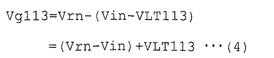
inverter 112 is designated by Vg112 and voltage at an input terminal of theinverter 113 by Vg113, since the electric charge stored in the capacitor in the sampling mode is preserved also in the amplifying mode, the voltages at the input terminals of the respective inverters in the amplifying mode are as shown below.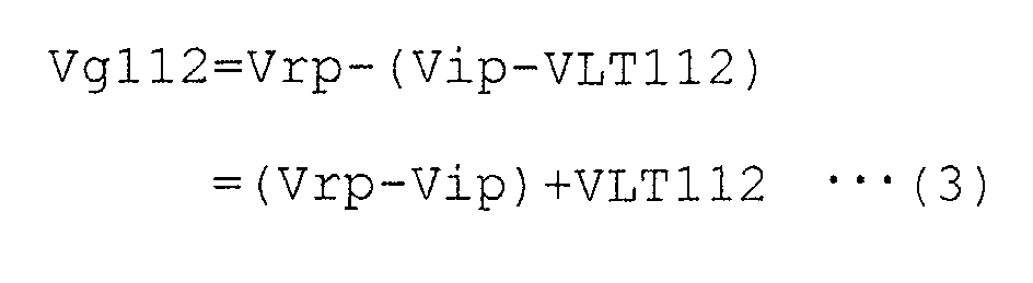
- Further, when the positive side voltage Vip and the negative side voltage Vin are represented by positive and negative analog input signals Vi with common mode voltage Vic of the analog input signal as a reference and the positive side voltage Vrp and the negative side voltage Vrn are represented by positive and negative reference voltage Vr with common mode voltage Vrc of the reference voltage as a reference, the following relationships are established.
- Hence, when Equations (5) through (8) are substituted for Equations (3) and (4), the following relationships are established.


- When the difference between Vg112 and Vg113 is calculated, although the difference between common mode voltage Vic and the common mode voltage Vrc is canceled, since in the amplifying mode, electric charge is not redistributed to the
capacitor 110 and thecapacitor 111, the input terminals of theinverters - In this way, according to the conventional balance type voltage comparing circuit, the input terminal of the inverter is applied with even the difference between the common mode voltage of the analog input signal and the common mode voltage of the reference voltage other than the difference between the analog input signal and the reference voltage and therefore, when the difference between the common mode voltage of the analog input signal and the common mode voltage of the reference voltage is increased, the output of the inverter is saturated. Therefore, no inbalance can be caused between the output voltages of the
inverters - When the inverter used in the voltage comparing circuit is ideal having no restriction on the output amplitude, even if the difference between the common mode voltage of the analog input signal and the common mode voltage of the reference voltage is applied to the input of the inverter, the output is not saturated and therefore, in the latch mode, the difference between the outputs of the inverters can be amplified and large or small between the analog input signal and the reference voltage can normally be determined. However, according to the actual inverter, the output amplitude of the inverter is limited and therefore, when the difference between the common mode voltage of the analog input signal and the common mode voltage of the reference voltage is increased, the output of the inverter is saturated and the difference between the outputs of the inverters is nullified and therefore, a problem occurs that in the latch mode, large or small between the analog input signal and the reference voltage cannot normally be determined.
- It is an object of the invention to provide a voltage comparing circuit capable of normally determining large or small between an analog input signal and reference voltage by canceling common mode voltages of the analog input signal and the reference voltage.
- A voltage comparing circuit of the invention includes a first and a second capacitor,terminals on one side of which are respectively connected to a positive side voltage of an analog input signal and a negative side voltage of a reference voltage via a first and a second switch and terminals on other side of which are commonly connected, a third and a fourth capacitor, terminals on one side of which are respectively connected to a positive side voltage of the reference voltage via a third and a fourth switch and a negative side voltage of the analog input signal and terminals on other side of which are commonly connected, a first and a second inverter respectively connected to a common connection terminal of the first and the second capacitors and a common connection terminal of the third and the fourth capacitors and connected with a fifth and a sixth switch respectively between input and output terminals thereof, a seventh and an eighth switch respectively connected between the input terminal of the first inverter and the output terminal of the second inverter and between the input terminal of the second inverter and the output terminal of the first inverter, and a ninth and a tenth switch respectively connected between the first capacitor and the fourth capacitor and between the second capacitor and the third capacitor.
- The above-mentioned and other objects, features and advantages of this invention will become more apparent by reference to the following detailed description of the invention taken in conjunction with the accompanying drawings, wherein:
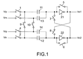
- FIG. 1 is a circuit diagram showing a first embodiment of a voltage comparing circuit according to the invention;
- FIGS. 2A through 2C are diagrams respectively showing operational states of respective switches in an input sampling mode, an amplifying mode and a latch mode of the embodiment of FIG. 1;
- FIG. 3 is a time chart showing the operational states of the respective switches in the respective operational modes of the embodiment of FIG. 1;
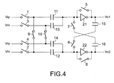
- FIG. 4 is a circuit diagram showing a second embodiment of the invention;
- FIGS. 5A through 5C are diagrams respectively showing operational states of respective switches in an input sampling mode, an amplifying mode and a latch mode of the embodiment of FIG. 4;
- FIG. 6 is a time chart showing the operational states of the respective switches in the respective operational modes of the embodiment of FIG. 4;
- FIG. 7 is a circuit diagram showing a voltage comparing circuit of a conventional example;
- FIGS. 8A through 8C are diagrams respectively showing operational states of respective switches in an input sampling mode, an amplifying mode and a latch mode of the voltage comparing circuit of FIG. 7;
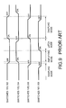
- FIG. 9 is a time chart showing the operational states of the respective switches in the respective operational modes of the voltage comparing circuit of FIG. 7; and
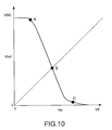
- FIG. 10 is a diagram showing a transfer characteristic of an inverter.
-
- Next, explanation will be given of the invention in reference to FIGS. 1 through 3 as follows.
-
Numerals 1 through 10 designate switches made ON and OFF respectively in accordance with operational modes, 11 through 14 respectively designate capacitors and 21 and 22 designate a pair of inverters. Further, Vip designates a positive side voltage of an analog input signal, Vin designates a negative side voltage of the analog input signal, Vrn designates negative side voltage of reference voltage and Vrp designates positive side voltage of the reference voltage. -
Switch 1 is connected between the positive side voltage Vip and thecapacitor 11,switch 2 is connected between the negative side voltage Vin andcapacitor 12,switch 3 is connected between the negative side voltage Vrn andcapacitor 13 andswitch 4 is connected between the positive side voltage Vrp andcapacitor 14. Terminals ofcapacitor 11 andcapacitor 13 andcapacitor 14 andcapacitor 12 on sides opposed to the switches are commonly connected, respectively. - Switch 5 is connected between input and output terminals of
inverter 21,switch 6 is connected between input and output terminals ofinverter 22,switch 7 is connected between the input terminal ofinverter 21 and the output terminal ofinverter 22 andswitch 8 is connected between the output terminal ofinverter 21 and the input terminal ofinverter 22. Further,switch 9 is connected between a connection point ofswitch 1 andcapacitor 11 and a connection point ofswitch 2 andcapacitor 12 andswitch 10 is connected between the connection point ofswitch 3 andcapacitor 13 and a connection point ofswitch 4 andcapacitor 14. - Next, detailed explanation will be given of specific operation of the embodiment in reference to FIG. 1 through FIG. 3. As shown by FIGS. 2A, 2B and 2C, operation of a voltage comparing circuit of FIG. 1 is classified into an input sampling mode, an amplifying mode and a latch mode. Explanation will be given of the operation for the respective modes as follows.
- First, in the case of the input sampling mode, as shown by FIG. 2A AND FIG. 3,
switches switches inverter 21 is storedincapacitor 11 and the difference between the negative side voltage Vrn and the logical threshold voltage VLT1 ofinverter 21 is stored incapacitor 13. Also, the difference between the negative side voltage Vin and logical threshold voltage VLP2 ofinverter 22 is stored incapacitor 12 and the difference between the positive side voltage Vrp and the logical threshold voltage of VLP2 ofinverter 22 is stored incapacitor 14. - In the transfer characteristic shown in FIG. 10, the logical threshold voltage indicates voltage at point B at which the input voltage Vin and the output voltage Vout are equal to each other and is voltage having an inherent value in the respective inverter and is specifically outputted when the input and the output of the inverter are shortcircuited.
- Next, when the amplifying mode is brought about, as shown by FIG. 2B and FIG. 3, switches 9 and 10 are made ON and switches 1, 2, 3, 4, 5, 6, 7 and 8 are made OFF. Thereby,
capacitor 11 andcapacitor 12 are connected in series and the series circuit is connected in parallel withcapacitors capacitors inverters inverter 21 amplifies a potential variation of the input terminal from logical threshold voltage VLT1,inverter 22 amplifies a potential variation of the input terminal from logical threshold voltage VLT2 and outputs Vol and Vo2 are respectively generated thereby. - Next, when the latch mode is brought about, as shown by FIG. 2C and FIG. 3, switches 7, 8, 9 and 10 are made ON and switches 1, 2, 3, 4, 5 and 6 are made OFF. Thereby,
inverters inverters - Finally, in the transfer characteristic between the input voltage Vin and the output voltage Vout of the inverter shown in FIG. 10, output voltage of one of the inverters is changed up to point A near to power source voltage VDD and output voltage of other of the inverters is changed up to point C near to ground voltage VE to thereby determine large or small between the analog input signal and the reference voltage . Thereafter, the input sampling mode, the amplifying mode and the latch mode are repeatedly carried out and at the respective time, large or small between the analog input signal and the reference voltage is determined.
- Explanation will be given of the principle of not effecting influence on the determination of large or small between the analog input signal and the reference voltage by removing the respective common mode voltages of the analog input signal and the reference voltage according to the embodiment in reference to equations.
- First, when electrostatic capacitance of the
capacitor 11 is designated by C11, electric charge stored incapacitor 11 by QC11, electrostatic capacitance of thecapacitor 12 by C12, electric charge stored incapacitor 12 by QC12, electrostatic capacitance ofcapacitor 13 by C13, electric charge stored incapacitor 13 by QC13, electrostatic capacitance ofcapacitor 14 by C14 and electric charge stored incapacitor 14 by Q14, electric charge stored in respective capacitors in the sampling mode is as follows. - When a voltage difference between an input terminal of
inverter 21 and an input terminal ofinverter 22 is designated by Vd, since electric charge stored in the capacitor in the samplingmode is preserved also in the amplifying mode, when electric charge stored incapacitors C C C C C C 
- When the logical threshold voltage VLT1 of
inverter 21 and logical threshold voltage VLT2 ofinverter 22 are made equal to each other, Equation (16)will read: - Further, when the positive side voltage Vip and the negative side voltage Vin are represented by positive and negative analog input signals Vi with common mode voltage Vic of the analog input signal as a reference and the positive side voltage Vrp and the negative side voltage Vrn are represented by positive and negative reference voltages Vr with common voltage Vrc of the reference voltage as a reference, as has been explained previously, the following relationships are established.
- Therefore, when Equations (5), (6), (7) and (8) are substituted for Equation (17), the following relationship is established.

- Therefore, as is apparent from Equation (18) the common mode voltage Vic and the common mode voltage Vrc can be canceled and only the difference between the analog input signal and the reference voltage emerges between the input terminals of
inverters - Further, since the analog input signal and the reference voltage are sampled at the same time, even when the logical threshold voltage of the inverter is varied by a variation in power source voltage or the like, influences thereby on the analog input signal and the reference voltage are made equal to each other and therefore, the capability is also effected to alleviate the influence of variation in the logical threshold voltage effected on determination of large or small between the analog input signal and the reference voltage.
- Next, explanation will be given of a second embodiment of the invention referring to FIG. 4 through FIG. 6.
-
Numerals 1 through 10 designate switches, 11 through 16 designate capacitors and 21 and 22 designate inverters. - According to the embodiment, what is different from the embodiment shown in FIG. 1 is that a
capacitor 15 is connected between an output of theinverter 21 and theswitch 8, acapacitor 16 is connected between an output ofinverter 22 andswitch 7 and a positive feedback loop formed byswitches capacitors - Next, detailed explanation will be given of operation of the embodiment referring to FIG. 4 through FIG. 6.
- Operation is carried out similar to that of the voltage comparing circuit of the first embodiment. Since
capacitors switch inverters - In this case, an input terminal of
inverter 21 is connected to the output terminal ofinverter 22 and an input terminal of theinverter 22 is connected to the output terminal ofinverter 21 respectively via the switches and the capacitors and therefore, voltage of the input terminal ofinverter 21 stays to be voltage produced by dividing voltage of the output terminal ofinverter 22 by capacitance ofcapacitor 16 and input capacitance of the input terminal ofinverter 21 and voltage at the input terminal ofinverter 22 stays to be voltage produced by dividing voltage at the output terminal ofinverter 21 by capacitance ofcapacitor 15 and input capacitance of the input terminal ofinverter 22. - Operation of a voltage comparing circuit according to the embodiment can be classified into an input sampling mode, an amplifying mode and a latch mode respectively shown by FIG. 5.
- Explanation will be given of the respective operational modes as follows.
- First, in the input sampling mode, as shown by FIG. 5A and FIG. 6, switches 1, 2, 3, 4, 5, 6, 7 and 8 are made ON and switches 9 and 10 are made OFF. Thereby, the difference between the positive side voltage Vip and the logical threshold voltage VLT1 of
inverter 21 is stored incapacitor 11 and the difference between the negative side voltage Vrn and logical threshold voltage VLT1 ofinverter 21 is stored incapacitor 13. Further, the difference between the negative side voltage Vin and the logical threshold voltage VLT2 ofinverter 22 is stored incapacitor 12, the difference between the positive side voltage Vrp and the logical threshold voltage VLT2 is stored incapacitor 14 and a difference between the logical threshold voltages VLT1 and VLT2 is stored incapacitors - Next, when the amplifying mode is brought about, as shown by FIG. 5B and FIG. 6, switches 9 and 10 are made ON and switches 1, 2, 3, 4, 5, 6, 7 and 8 are made OFF. Thereby,
capacitor 11 andcapacitor 12 are connected in series and the series circuit is connected in parallel withcapacitors capacitors inverters inverter 21 amplifies the potential variation from logical threshold voltage VLT1 of the input terminal,inverter 22 amplifies the potential variation from logical threshold voltage VLT2 of the input terminal and outputs Vo1 and Vo2 are generated respectively thereby. - In the latch mode, as shown by FIG. 5C and FIG. 6, switches 7, 8, 9 and 10 are made ON and switches 1, 2, 3, 4, 5 and 6 are made OFF. Thereby,
inverters capacitors inverters - According to the embodiment, similar to the first embodiment, large or small between the analog input signal Vi and the reference voltage Vr can be determined without being effected with influence on common mode voltage of the analog input signal and the common mode voltage of the reference voltage . Further, by operation of
capacitors switches inverters inverters - Further, constant current circuits may be inserted between power source inputs and power sources of the
inverters inverters - As has been explained above, according to the invention, by canceling the common mode voltage of the analog input signal and the common mode voltage of the reference voltage, large or small between the analog input signal and the reference voltage can be determined without being effected with influence of the common mode voltages. Further, by inserting the capacitors to the positive feedback loop, the time period necessary for sampling can be shortened and the operation can be carried out at high speed.
- Although the invention has been described with reference to specific embodiments, this description is not meant to be construed in a limiting sense. Various modifications of the disclosed embodiments will become apparent to persons skilled in the art upon reference to the description of the invention. It is therefore contemplated that the appended claims will cover any modifications or embodiments as fall within the true scope of the invention.
Claims (5)
- A voltage comparing circuit comprising:wherein said voltage comparing circuit respectively includes a first mode of turning all of the switches excluding the ninth and the tenth switches on, a second mode of turning the ninth and the tenth switches on and turning remaining ones of the switches off and a third mode of turning the seventh through the tenth switch on and turningthe first through the sixth switches off.a first and a second capacitor, terminals on one side of which are respectively connected to a positive side voltage of an analog input signal and a negative side voltage of a reference voltage via a first and a second switch and terminals on other side of which are commonly connected;a third and a fourth capacitor, terminals on one side of which are respectively connected to a positive side voltage of the reference voltage and a negative side voltage of the analog input signal via a third and a fourth switch and terminals on other side of which are commonly connected;a first and a second inverter respectively connected to a common connection terminal of the first and the second capacitors and a common connection terminal of the third and the fourth capacitors and connected with a fifth and a sixth switch respectively between input and output terminals thereof;a seventh and an eighth switch respectively connected between the input terminal of the first inverter and the output terminal of the second inverter and between the input terminal of the second inverter and the output terminal of the first inverter; anda ninth and a tenth switch respectively connected between the first capacitor and the fourth capacitor and between the second capacitor and the third capacitor;
- The voltage comparing circuit according to Claim 1,
wherein the seventh and the eighth switches are respectively connected in series with a fifth and a sixth capacitor. - The voltage comparing circuit according to Claim 1,
wherein the first operational mode, the second operational and the third operational mode are repeatedly carried out and at respective times thereof, a result of comparing the analog input signal and the reference voltage is outputted from outputs of the first and the second inverters. - The voltage comparing circuit according to Claim 1,
wherein a common mode voltage of the analog input signal and a common mode voltage of the reference voltage are removed by connecting in parallel a series circuit of the first capacitor and the fourth capacitor and a series circuit of the second capacitor and the third capacitor by turning the ninth and the tenth switches on in the second operational mode. - The voltage comparing circuit according to Claim 1,
wherein constant current circuits are inserted between power source inputs and power sources of the first and the second inverters.
Applications Claiming Priority (2)
| Application Number | Priority Date | Filing Date | Title |
|---|---|---|---|
| JP2001180286 | 2001-06-14 | ||
| JP2001180286A JP3616353B2 (en) | 2001-06-14 | 2001-06-14 | Voltage comparison circuit |
Publications (2)
| Publication Number | Publication Date |
|---|---|
| EP1267492A1 true EP1267492A1 (en) | 2002-12-18 |
| EP1267492B1 EP1267492B1 (en) | 2004-11-03 |
Family
ID=19020728
Family Applications (1)
| Application Number | Title | Priority Date | Filing Date |
|---|---|---|---|
| EP20020090213 Expired - Lifetime EP1267492B1 (en) | 2001-06-14 | 2002-06-12 | Voltage comparing circuit |
Country Status (7)
| Country | Link |
|---|---|
| US (1) | US6559688B2 (en) |
| EP (1) | EP1267492B1 (en) |
| JP (1) | JP3616353B2 (en) |
| KR (1) | KR100450165B1 (en) |
| CN (1) | CN1321498C (en) |
| DE (1) | DE60201778T2 (en) |
| TW (1) | TWI262651B (en) |
Families Citing this family (12)
| Publication number | Priority date | Publication date | Assignee | Title |
|---|---|---|---|---|
| JP4837673B2 (en) * | 2005-11-21 | 2011-12-14 | パナソニック株式会社 | Fully differential amplifier circuit |
| JP4939096B2 (en) * | 2006-04-04 | 2012-05-23 | ルネサスエレクトロニクス株式会社 | Amplifier and drive circuit using the same |
| JP4961159B2 (en) * | 2006-04-14 | 2012-06-27 | オリンパス株式会社 | Amplifier circuit and its application circuit |
| US7724170B2 (en) * | 2007-12-02 | 2010-05-25 | The Chinese University Of Hong Kong | Sensor interface devices and amplifiers |
| JP5104383B2 (en) * | 2008-02-20 | 2012-12-19 | 富士通株式会社 | Electronic circuit equipment |
| CN101540598B (en) * | 2008-03-21 | 2011-07-06 | 盛群半导体股份有限公司 | Improved comparator circuit architecture for low voltage output |
| US8198920B2 (en) * | 2009-03-23 | 2012-06-12 | Atmel Corporation | Low current comparator with programmable hysteresis |
| JP6503198B2 (en) * | 2015-03-05 | 2019-04-17 | エイブリック株式会社 | Comparison circuit and sensor device |
| DE102017216667A1 (en) * | 2017-09-20 | 2019-03-21 | Robert Bosch Gmbh | Apparatus and method for generating a differential voltage |
| CN209803679U (en) * | 2019-07-11 | 2019-12-17 | 京东方科技集团股份有限公司 | a automatic wake-up circuit, wearable equipment for wearable equipment |
| JP7356866B2 (en) * | 2019-10-31 | 2023-10-05 | ローム株式会社 | voltage comparator |
| KR20230159144A (en) * | 2022-05-13 | 2023-11-21 | 삼성전자주식회사 | Comparator circuit including feadback circuit |
Citations (4)
| Publication number | Priority date | Publication date | Assignee | Title |
|---|---|---|---|---|
| US5546028A (en) * | 1994-09-07 | 1996-08-13 | Nec Corporation | Chopper type comparator for an analog-to-digital converter |
| US5684485A (en) * | 1994-07-18 | 1997-11-04 | Thomson Multimedia S.A. | Multi-comparison analog-to-digital converters using the interpolation principle |
| EP0831592A1 (en) * | 1996-09-20 | 1998-03-25 | Nec Corporation | Chopper comparator showing high speed and low power operations free of malfunction under variation of logical threshold voltage of invertor |
| EP0939489A2 (en) * | 1998-02-27 | 1999-09-01 | NEC Corporation | Chopper voltage comparator circuit and method |
Family Cites Families (10)
| Publication number | Priority date | Publication date | Assignee | Title |
|---|---|---|---|---|
| JPS61200715A (en) * | 1985-03-01 | 1986-09-05 | Nippon Telegr & Teleph Corp <Ntt> | Voltage comparator |
| JPH03105862A (en) | 1989-09-19 | 1991-05-02 | Japan Storage Battery Co Ltd | Clad type lead-acid battery |
| JP3031486B2 (en) * | 1990-11-30 | 2000-04-10 | 日本テキサス・インスツルメンツ株式会社 | Differential chopper comparator |
| US5332931A (en) * | 1991-06-24 | 1994-07-26 | Harris Corporation | High speed differential comparator |
| JP2762868B2 (en) * | 1992-09-29 | 1998-06-04 | 日本電気株式会社 | Voltage comparison circuit |
| JP3222276B2 (en) * | 1993-07-30 | 2001-10-22 | セイコーインスツルメンツ株式会社 | Comparator circuit and control method of comparator circuit |
| JP3709640B2 (en) * | 1996-12-27 | 2005-10-26 | ソニー株式会社 | Voltage comparison circuit and analog / digital conversion circuit using the same |
| JPH10256884A (en) * | 1997-03-12 | 1998-09-25 | Mitsubishi Electric Corp | Voltage comparator and A / D converter |
| JP3439322B2 (en) * | 1997-06-17 | 2003-08-25 | Necエレクトロニクス株式会社 | Differential input chopper type voltage comparison circuit |
| JPH11308082A (en) * | 1998-04-20 | 1999-11-05 | Texas Instr Japan Ltd | Chopper type comparator |
-
2001
- 2001-06-14 JP JP2001180286A patent/JP3616353B2/en not_active Expired - Fee Related
-
2002
- 2002-06-06 TW TW091112235A patent/TWI262651B/en not_active IP Right Cessation
- 2002-06-10 US US10/166,316 patent/US6559688B2/en not_active Expired - Fee Related
- 2002-06-12 DE DE60201778T patent/DE60201778T2/en not_active Expired - Fee Related
- 2002-06-12 EP EP20020090213 patent/EP1267492B1/en not_active Expired - Lifetime
- 2002-06-13 CN CNB021232202A patent/CN1321498C/en not_active Expired - Fee Related
- 2002-06-14 KR KR10-2002-0033191A patent/KR100450165B1/en not_active Expired - Fee Related
Patent Citations (4)
| Publication number | Priority date | Publication date | Assignee | Title |
|---|---|---|---|---|
| US5684485A (en) * | 1994-07-18 | 1997-11-04 | Thomson Multimedia S.A. | Multi-comparison analog-to-digital converters using the interpolation principle |
| US5546028A (en) * | 1994-09-07 | 1996-08-13 | Nec Corporation | Chopper type comparator for an analog-to-digital converter |
| EP0831592A1 (en) * | 1996-09-20 | 1998-03-25 | Nec Corporation | Chopper comparator showing high speed and low power operations free of malfunction under variation of logical threshold voltage of invertor |
| EP0939489A2 (en) * | 1998-02-27 | 1999-09-01 | NEC Corporation | Chopper voltage comparator circuit and method |
Also Published As
| Publication number | Publication date |
|---|---|
| CN1321498C (en) | 2007-06-13 |
| KR100450165B1 (en) | 2004-09-30 |
| CN1392668A (en) | 2003-01-22 |
| DE60201778T2 (en) | 2005-12-15 |
| US20020196054A1 (en) | 2002-12-26 |
| JP2002374153A (en) | 2002-12-26 |
| TWI262651B (en) | 2006-09-21 |
| KR20020095446A (en) | 2002-12-26 |
| JP3616353B2 (en) | 2005-02-02 |
| EP1267492B1 (en) | 2004-11-03 |
| DE60201778D1 (en) | 2004-12-09 |
| US6559688B2 (en) | 2003-05-06 |
Similar Documents
| Publication | Publication Date | Title |
|---|---|---|
| US5448056A (en) | Photoelectric converting circuit having an amplification factor | |
| EP1267492B1 (en) | Voltage comparing circuit | |
| US11863132B2 (en) | Switched capacitor amplifier circuit, voltage amplification method, and infrared sensor device | |
| CN100542043C (en) | Successive approximation analog to digital converter | |
| JP3092525B2 (en) | Chopper type comparator | |
| JPH08273388A (en) | Sample hold circuit | |
| US20090179787A1 (en) | Comparator and a/d converter | |
| JPH02228812A (en) | Comparator | |
| JP3105862B2 (en) | Voltage comparison circuit | |
| US6756928B2 (en) | Pseudo-differential amplifier and analog-to-digital converter using the same | |
| US8773198B2 (en) | Auto-zero amplifier and sensor module using same | |
| JPH10327072A (en) | Analog / digital converter and voltage comparator | |
| US20020180528A1 (en) | Cmos folding amplifier having high resolution and low power consumption | |
| JP3916560B2 (en) | Capacitor switching pipeline analog-digital converter | |
| JP2005057627A (en) | Peak detection circuit | |
| KR100246345B1 (en) | Voltage comparator | |
| JP2531071B2 (en) | Image sensor drive | |
| Christoforou | A chopper-based CMOS current sense instrumentation amplifier [for GSM] | |
| KR950000770Y1 (en) | Multistage Sample, Hold Circuit | |
| KR890000948B1 (en) | Digital information signal split integrated circuit | |
| KR890004061B1 (en) | Integral circuit for separating digital signals from complete video signals | |
| JPH06273457A (en) | Voltage comparator | |
| JPH01181220A (en) | Voltage comparison circuit | |
| JPH03188710A (en) | Chopper amplifier circuit | |
| JPH0743396A (en) | Chopper type voltage comparator |
Legal Events
| Date | Code | Title | Description |
|---|---|---|---|
| PUAI | Public reference made under article 153(3) epc to a published international application that has entered the european phase |
Free format text: ORIGINAL CODE: 0009012 |
|
| AK | Designated contracting states |
Kind code of ref document: A1 Designated state(s): AT BE CH CY DE DK ES FI FR GB GR IE IT LI LU MC NL PT SE TR |
|
| AX | Request for extension of the european patent |
Free format text: AL;LT;LV;MK;RO;SI |
|
| 17P | Request for examination filed |
Effective date: 20021128 |
|
| RAP1 | Party data changed (applicant data changed or rights of an application transferred) |
Owner name: NEC ELECTRONICS CORPORATION |
|
| AKX | Designation fees paid |
Designated state(s): DE FR GB NL |
|
| GRAP | Despatch of communication of intention to grant a patent |
Free format text: ORIGINAL CODE: EPIDOSNIGR1 |
|
| GRAS | Grant fee paid |
Free format text: ORIGINAL CODE: EPIDOSNIGR3 |
|
| GRAA | (expected) grant |
Free format text: ORIGINAL CODE: 0009210 |
|
| AK | Designated contracting states |
Kind code of ref document: B1 Designated state(s): DE FR GB NL |
|
| REG | Reference to a national code |
Ref country code: GB Ref legal event code: FG4D |
|
| REF | Corresponds to: |
Ref document number: 60201778 Country of ref document: DE Date of ref document: 20041209 Kind code of ref document: P |
|
| REG | Reference to a national code |
Ref country code: IE Ref legal event code: FG4D |
|
| PLBE | No opposition filed within time limit |
Free format text: ORIGINAL CODE: 0009261 |
|
| STAA | Information on the status of an ep patent application or granted ep patent |
Free format text: STATUS: NO OPPOSITION FILED WITHIN TIME LIMIT |
|
| ET | Fr: translation filed | ||
| 26N | No opposition filed |
Effective date: 20050804 |
|
| PGFP | Annual fee paid to national office [announced via postgrant information from national office to epo] |
Ref country code: GB Payment date: 20060607 Year of fee payment: 5 |
|
| PGFP | Annual fee paid to national office [announced via postgrant information from national office to epo] |
Ref country code: DE Payment date: 20060608 Year of fee payment: 5 Ref country code: FR Payment date: 20060608 Year of fee payment: 5 |
|
| PGFP | Annual fee paid to national office [announced via postgrant information from national office to epo] |
Ref country code: NL Payment date: 20060615 Year of fee payment: 5 |
|
| GBPC | Gb: european patent ceased through non-payment of renewal fee |
Effective date: 20070612 |
|
| NLV4 | Nl: lapsed or anulled due to non-payment of the annual fee |
Effective date: 20080101 |
|
| REG | Reference to a national code |
Ref country code: FR Ref legal event code: ST Effective date: 20080229 |
|
| PG25 | Lapsed in a contracting state [announced via postgrant information from national office to epo] |
Ref country code: NL Free format text: LAPSE BECAUSE OF NON-PAYMENT OF DUE FEES Effective date: 20080101 Ref country code: DE Free format text: LAPSE BECAUSE OF NON-PAYMENT OF DUE FEES Effective date: 20080101 |
|
| PG25 | Lapsed in a contracting state [announced via postgrant information from national office to epo] |
Ref country code: GB Free format text: LAPSE BECAUSE OF NON-PAYMENT OF DUE FEES Effective date: 20070612 |
|
| PG25 | Lapsed in a contracting state [announced via postgrant information from national office to epo] |
Ref country code: FR Free format text: LAPSE BECAUSE OF NON-PAYMENT OF DUE FEES Effective date: 20070702 |