EP1267416A1 - Nonvolatile storage device and method for manufacturing nonvolatile storage device - Google Patents
Nonvolatile storage device and method for manufacturing nonvolatile storage device Download PDFInfo
- Publication number
- EP1267416A1 EP1267416A1 EP01999009A EP01999009A EP1267416A1 EP 1267416 A1 EP1267416 A1 EP 1267416A1 EP 01999009 A EP01999009 A EP 01999009A EP 01999009 A EP01999009 A EP 01999009A EP 1267416 A1 EP1267416 A1 EP 1267416A1
- Authority
- EP
- European Patent Office
- Prior art keywords
- gate electrode
- nonvolatile memory
- memory element
- floating gate
- interlayer dielectric
- Prior art date
- Legal status (The legal status is an assumption and is not a legal conclusion. Google has not performed a legal analysis and makes no representation as to the accuracy of the status listed.)
- Withdrawn
Links
Images






Classifications
-
- H—ELECTRICITY
- H10—SEMICONDUCTOR DEVICES; ELECTRIC SOLID-STATE DEVICES NOT OTHERWISE PROVIDED FOR
- H10D—INORGANIC ELECTRIC SEMICONDUCTOR DEVICES
- H10D30/00—Field-effect transistors [FET]
- H10D30/60—Insulated-gate field-effect transistors [IGFET]
- H10D30/68—Floating-gate IGFETs
- H10D30/681—Floating-gate IGFETs having only two programming levels
- H10D30/683—Floating-gate IGFETs having only two programming levels programmed by tunnelling of carriers, e.g. Fowler-Nordheim tunnelling
-
- H—ELECTRICITY
- H10—SEMICONDUCTOR DEVICES; ELECTRIC SOLID-STATE DEVICES NOT OTHERWISE PROVIDED FOR
- H10D—INORGANIC ELECTRIC SEMICONDUCTOR DEVICES
- H10D30/00—Field-effect transistors [FET]
- H10D30/01—Manufacture or treatment
- H10D30/021—Manufacture or treatment of FETs having insulated gates [IGFET]
- H10D30/0411—Manufacture or treatment of FETs having insulated gates [IGFET] of FETs having floating gates
-
- H—ELECTRICITY
- H10—SEMICONDUCTOR DEVICES; ELECTRIC SOLID-STATE DEVICES NOT OTHERWISE PROVIDED FOR
- H10D—INORGANIC ELECTRIC SEMICONDUCTOR DEVICES
- H10D30/00—Field-effect transistors [FET]
- H10D30/01—Manufacture or treatment
- H10D30/021—Manufacture or treatment of FETs having insulated gates [IGFET]
- H10D30/0413—Manufacture or treatment of FETs having insulated gates [IGFET] of FETs having charge-trapping gate insulators, e.g. MNOS transistors
-
- H—ELECTRICITY
- H10—SEMICONDUCTOR DEVICES; ELECTRIC SOLID-STATE DEVICES NOT OTHERWISE PROVIDED FOR
- H10D—INORGANIC ELECTRIC SEMICONDUCTOR DEVICES
- H10D30/00—Field-effect transistors [FET]
- H10D30/60—Insulated-gate field-effect transistors [IGFET]
- H10D30/68—Floating-gate IGFETs
- H10D30/681—Floating-gate IGFETs having only two programming levels
-
- H—ELECTRICITY
- H10—SEMICONDUCTOR DEVICES; ELECTRIC SOLID-STATE DEVICES NOT OTHERWISE PROVIDED FOR
- H10D—INORGANIC ELECTRIC SEMICONDUCTOR DEVICES
- H10D30/00—Field-effect transistors [FET]
- H10D30/60—Insulated-gate field-effect transistors [IGFET]
- H10D30/68—Floating-gate IGFETs
- H10D30/6891—Floating-gate IGFETs characterised by the shapes, relative sizes or dispositions of the floating gate electrode
-
- H—ELECTRICITY
- H10—SEMICONDUCTOR DEVICES; ELECTRIC SOLID-STATE DEVICES NOT OTHERWISE PROVIDED FOR
- H10D—INORGANIC ELECTRIC SEMICONDUCTOR DEVICES
- H10D64/00—Electrodes of devices having potential barriers
- H10D64/01—Manufacture or treatment
- H10D64/031—Manufacture or treatment of data-storage electrodes
- H10D64/035—Manufacture or treatment of data-storage electrodes comprising conductor-insulator-conductor-insulator-semiconductor structures
-
- H—ELECTRICITY
- H10—SEMICONDUCTOR DEVICES; ELECTRIC SOLID-STATE DEVICES NOT OTHERWISE PROVIDED FOR
- H10D—INORGANIC ELECTRIC SEMICONDUCTOR DEVICES
- H10D64/00—Electrodes of devices having potential barriers
- H10D64/01—Manufacture or treatment
- H10D64/031—Manufacture or treatment of data-storage electrodes
- H10D64/037—Manufacture or treatment of data-storage electrodes comprising charge-trapping insulators
Definitions
- the present invention relates to a nonvolatile memory element retaining data regardless of whether its power supply is on or off and a method of manufacturing the nonvolatile memory element, and in particular to a nonvolatile memory element configured to be of FG type and a method of manufacturing the nonvolatile memory element.
- nonvolatile memory elements capable of retaining data regardless of whether power supplies thereof are on or off have been used as memory elements to retain data.
- nonvolatile memory elements are typically an FG (Floating Gate) type nonvolatile memory element and a MONOS (Metal - Si oxide film - Si nitride film - Si substrate) type nonvolatile memory element. Both elements charge to store information in a given method.
- Such an FG type nonvolatile memory element is configured to provide a floating gate electrode of polycrystalline Si, for example, in an intermediate position within a gate insulating film of an MIS type transistor. By charging the floating gate electrode, a threshold of the MIS type transistor is changed so as to store information.
- Figs. 8A to 8D and Figs. 9A to 9C are cross-sectional views for explaining a process of manufacturing an FG type nonvolatile memory element 100 of a conventional design.
- an element isolation layer 102 is formed in a Si substrate 101 by means of shallow trench isolation and the like, then an embedded layer 103 for adjusting a threshold voltage is formed by means of a conventional ion implantation process.
- the Si substrate 101 is thermally oxidized at about 800°C for about 15 minutes so that, as shown in Fig. 8B, a tunnel oxide film 104 having a thickness of about 8 nm is formed on a surface of the Si substrate 101. Then, a floating gate electrode 105 is formed on a surface thereof to have a thickness of about 6 nm, further an interlayer dielectric 106 is formed on a surface thereof.
- Fig. 8C is an enlarged view showing a detailed construction of the tunnel oxide film 104, the floating gate electrode 105 and the interlayer dielectric 106 which are configured as described above.
- the interlayer dielectric 106 has a three-layer construction of a Si oxide film 106a, a Si nitride film 106b and a Si oxide film 106c.
- the Si oxide film 106a is formed by performing thermal oxidation on a surface of the floating gate electrode 105 at about 850°C for about 10 minutes so as to have a thickness of about 5 nm.
- the Si nitride film 106b is formed by conventional processes such as an LP-CVD, plasma CVD on a surface of the Si oxide film 106a such that the Si nitride film 106b may be deposited up to about 12 nm.
- the Si oxide film 106c is formed by thermal oxidation of a surface of the Si nitride film 106b so as to have a thickness of about 6 nm.
- a control electrode 107 is formed of polycrystalline Si, WSi, etc. including a high concentration of phosphorus and the like, then patterned by means of a conventional lithographic technology and an RIE technology so as to be the control electrode 107 as shown in Fig. 9A. Further, using the patterned control electrode 107 as a mask, impurities such as phosphorus, arsenic, etc. are implanted by an ion implantation process at a concentration of 5 ⁇ 10 13 /cm 2 , for example, so as to form low concentration drains 108a and 108b.
- gate sidewalls 109 are formed by means of conventional CVD and etch back processes. Using the gate sidewalls 109 as masks, impurities such as phosphorus, arsenic, etc. are implanted by an ion implantation process at a concentration of 5 ⁇ 10 15 /cm 2 , for example, so as to form a source 110a and a drain 110b.
- heat treatment at about 900°C for about 30 minutes by means of a conventional electric heating furnace or heat treatment at about 1050°C for 10 seconds by means of rapid thermal processing (RTP) is carried out to form an interlayer film 111 of Si oxide film etc. and a plug 112 of W or polycrystalline Si to thereby construct the nonvolatile memory element 100 as shown in Fig. 9C.
- the nonvolatile memory element 100 As to the nonvolatile memory element 100, a voltage of about + 20 V is applied to the control electrode 107 in a situation where the Si substrate 101 is grounded so that, through a conduction channel area of the Si substrate 101, charges are injected into and stored in the floating gate electrode 105 by employing FN tunnel current or the like. In the state of the stored charges, a threshold voltage of the MIS type transistor is high. The state of the stored charges is maintained even after the voltage application to the control electrode 107 has been stopped. Thus, the nonvolatile memory element 100 can retain data regardless of whether power supply for the element is on or off.
- the MONOS type nonvolatile memory element has layers comprised of metal- Si oxide film - Si nitride film - Si oxide film - Si substrate. Charges are stored in discrete traps which are in the Si nitride film and near the boundary of the Si oxide film and the Si nitride film so as to change threshold values of transistors and to retain data (IE3 Trans, Electron Dev. ED39(2), 122(1983)).
- Figs. 10A to 10C and Figs. 11A to 11C are cross-sectional views for explaining a process of manufacturing a MONOS type nonvolatile memory element 200.
- an element isolation layer 202 is formed in a Si substrate 201 by means of shallow trench isolation and the like, then an embedded layer 203 for adjusting a threshold voltage is formed by means of a conventional ion implantation process.
- the Si substrate 201 is thermally oxidized at about 800°C for about 15 minutes so that a tunnel oxide film 204, about 3 nm thick, is formed on a surface of the Si substrate 201.
- a Si nitride film 205 is formed on a surface thereof by means of conventional processes such as an LP-CVD, a plasma CVD so as to have a thickness of about 8 nm.
- the Si nitride film 205 is oxidized again in order to form a Si oxide film 206 of about 3 to 5 nm.
- a control electrode 207 is formed of polycrystalline Si, WSi, etc. including a high concentration of phosphorus and the like, then patterned by means of conventional lithographic technology and RIE technology so as to be the control electrode 207 as shown in Fig. 11B.
- impurities such as phosphorus, arsenic, etc. are implanted by an ion implantation process at a concentration of 5 ⁇ 10 13 /cm 2 , for example, so as to form low concentration drains 208a and 208b as shown in Fig. 11C.
- gate sidewalls 209 are formed by means of conventional CVD and etch back processes. Using the gate sidewalls 209 as masks, impurities such as phosphorus, arsenic, etc. are implanted by an ion implantation process at a concentration of 5 ⁇ 10 15 /cm 2 , for example, so as to form a source 210a and a drain 210b.
- heat treatment at about 900°C for about 30 minutes by means of a conventional electric heating furnace or heat treatment at about 1050°C for 10 seconds by means of rapid thermal processing (RTP) is carried out to form an interlayer film 211 of Si oxide film etc. and a plug 212 of W or polycrystalline Si to thereby construct the nonvolatile memory element 200.
- traps to store charges are formed in the Si nitride film 205 itself and in a SiON transition layer located near the boundary of the Si oxide film 206 and the Si nitride film 205; the charges are discretely stored in the traps so as to retain data regardless of whether power supply for the element is on or off.
- the MONOS type nonvolatile memory element 200 discretely stores charges in traps which are in the tunnel oxide film 204 and the SiON transition layer near the boundary between the Si oxide film 206 and Si nitride film 205 so as to retain data, a partial leakage at the tunnel oxide film 204 does not lose all the charges stored in the traps. Therefore, the tunnel oxide film 204 may have a small thickness so that a data write voltage may be reduced and the element may be miniaturized compared with the FG type nonvolatile memory element 100.
- a trap density of the MONOS type nonvolatile memory element 200 is not sufficiently high.
- a density of charges to be stored is lower, by about five digits, than that of the FG type nonvolatile memory element 100.
- the nonvolatile memory element 200 it is not easy to form its traps to allow a good reproducibility of the density and a good controllability. There may be introduced a problem that the nonvolatile memory element 200 of a fine structure does not provide sufficient data retention time or sufficient endurance characteristics of write/erase.
- the present invention has been made so as to provide a nonvolatile memory element which ensures sufficient density of stored charges, data retention time, and endurance characteristics of write/erase, and at the same time enables a write voltage to decrease and the element itself to be smaller, and to provide a method of manufacturing the nonvolatile memory element.
- the present invention provides, in a nonvolatile memory element which retains data regardless of whether power supply for the element is on or off, the nonvolatile memory element characterized by comprising a semiconductor substrate to be a base; a tunnel oxide film formed on the semiconductor substrate; a floating gate electrode formed on the tunnel oxide film so as to have an irregular shape on its own surface; an interlayer dielectric formed on the floating gate electrode; and a control electrode formed on the interlayer dielectric.
- the surface of the floating gate electrode is formed to have the irregular shape so that a surface area of the floating gate electrode is larger, whereby a static capacity between the control electrode and the floating gate electrode can be increased.
- a ratio (a coupling ratio) of the static capacity between the control electrode and the floating gate electrode to the whole static capacity of the floating gate electrode can be increased so that an applied voltage between the semiconductor substrate and the floating gate electrode can be increased without increasing a voltage applied to the whole nonvolatile memory element.
- the irregular shape of the floating gate electrode may preferably be in an irregular shape on a substantially hemisphere.
- the irregular shape of the floating gate electrode is preferably formed so that a grain size may be 10 nm to 20 nm.
- the interlayer dielectric is preferably formed by means of an atomic layer chemical vapor deposition process.
- the floating gate electrode and the interlayer dielectric are preferably formed so as to surround a bottom surface and sidewalls of the control electrode.
- the nonvolatile memory element according to the present invention is preferably for a flash memory.
- a tunnel oxide film forming step of forming a tunnel oxide film on a Si substrate to be a base characterized by comprising a tunnel oxide film forming step of forming a tunnel oxide film on a Si substrate to be a base; a floating gate electrode forming step of forming, on the tunnel oxide film, a floating gate electrode having a surface of an irregular shape; an interlayer dielectric forming step of forming an interlayer dielectric on the floating gate electrode; a control electrode forming step of forming a control electrode on the interlayer dielectric.
- the surface of the floating gate electrode is formed in the irregular shape so that a surface area of the floating gate electrode is larger, whereby a static capacity between the control electrode and the floating gate electrode can be increased.
- a ratio (a coupling ratio) of the static capacity between the control electrode and the floating gate electrode to the whole static capacity of the floating gate electrode can be increased so that an applied voltage between the semiconductor substrate and the floating gate electrode can be increased without increasing a voltage applied to the whole nonvolatile memory element.
- the interlayer dielectric is preferably formed by means of an atomic layer chemical vapor deposition process in the interlayer dielectric forming step.
- the method of manufacturing the nonvolatile memory element according to the present invention preferably further comprises, in order to form a gate electrode, a gate electrode etching step of etching the tunnel oxide film, the floating gate electrode, the interlayer dielectric and the control electrode respectively formed by the tunnel oxide film forming step, the floating gate electrode forming step, the interlayer dielectric forming step and the control electrode forming step.
- the method of manufacturing the nonvolatile memory element according to the present invention preferably further comprises a dummy gate electrode forming step of forming a dummy gate electrode on the tunnel oxide film subsequent to the tunnel oxide film forming step; a dummy gate electrode etching step of etching the dummy gate electrode; a gate sidewall forming step of covering a sidewall of the dummy gate electrode with a gate sidewall; a dummy gate electrode removing step of removing the dummy gate electrode subsequent to forming the gate sidewall.
- the floating gate electrode forming step the floating gate electrode is formed along an inner sidewall of the gate sidewall.
- the interlayer dielectric forming step the interlayer dielectric is formed along an inner sidewall of the floating gate electrode.
- Figs. 1A to 1B are structural views showing a structure of a nonvolatile memory element 1.
- Fig. 1A shows a cross-sectional view of the nonvolatile memory element 1
- Fig. 1B shows an enlarged cross-sectional view of a portion A in Fig. 1A.
- the nonvolatile memory element 1 is an FG type nonvolatile memory element which is utilized as a flash memory, for example, and is mainly comprised of a Si substrate 2 which is a semiconductor substrate to be a base; an element isolation layer 3; an embedded layer 4 provided in the Si substrate 2 so as to adjust a threshold voltage; a tunnel oxide film 5 formed on the Si substrate 2; a floating gate electrode 6 formed on the tunnel oxide film 5 so as to have an irregular shape on its own surface; an interlayer dielectric 7 formed on the floating gate electrode 6; a control electrode 8 provided on the interlayer dielectric 7; low concentration drains 9a and 9b formed at a surface of the Si substrate 2; a source 11a; a drain 11b; a gate sidewall 10 formed on an upper surface of the Si substrate 2; an interlayer film 12; and a plug 13.
- the floating gate electrode 6 of the nonvolatile memory element 1 is formed to have the irregular shape on its own surface so that a surface area of the floating gate electrode 6 is increased and a static capacity between the floating gate electrode 6 and the control electrode 8 can be increased.
- the irregular shape may be of a substantial hemisphere such as a mushroom shape, a waveform, or any other rugged shape, however, the surface area of the resulting floating gate electrode 6 preferably has constant accuracy.
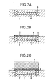
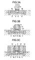
- Figs. 2A to 2C and Figs. 3A to 3C are cross-sectional structural views for explaining the process of manufacturing the nonvolatile memory element 1.
- the process of manufacturing the nonvolatile memory element 1 is mainly comprised of a tunnel oxide film forming step of forming the tunnel oxide film 5 on the Si substrate 2 which is a semiconductor substrate to be a base; a floating gate electrode forming step of forming, on the tunnel oxide film 5, the floating gate electrode 6 having an irregular shape on its own surface; an interlayer dielectric forming step of forming the interlayer dielectric 7 on the floating gate electrode 6; a control electrode forming step of forming the control electrode 8 on the interlayer dielectric 7; a gate electrode etching step of etching, in order to form a gate electrode, the tunnel oxide film 5, the floating gate electrode 6, the interlayer dielectric 7 and the control electrode 8; a low concentration drain forming step of forming the low concentration drains 9a and 9b; a gate sidewall forming step of forming the gate sidewall 10; a source and drain forming step of forming the source 11a and the drain 11b; an interlayer film forming step of forming the interlayer film 12; and a plug
- the element isolation layer 3 is formed in the Si substrate 2 by means of shallow trench isolation and the like, then the embedded layer 4 for adjusting a threshold voltage is formed by means of a conventional ion implantation process.
- the Si substrate 2 is thermally oxidized at about 800°C for about 15 minutes so that, as shown in Fig. 2B, the tunnel oxide film 5 having a thickness of about 8 nm is formed on a surface of the Si substrate 2 (the tunnel oxide film forming step).
- polycrystalline Si or the like is deposited on the tunnel oxide film 5 by means of a chemical vapor deposition (CVD) process which is carried out in a situation where oxygen is removed from an air-tight CVD apparatus, so that the floating gate electrode 6 having an irregular shape of a substantial hemisphere (hemispherical polysicon: Hemispherical Grain) on its own surface as shown in Fig. 1B is formed (the floating gate electrode forming step).
- CVD chemical vapor deposition
- an amorphous silicon is deposited on a surface of the tunnel oxide film 5 at a temperature of about 550°C for about 40 minutes by means of a chemical vapor deposition (CVD) process using silane (SiH 4 ) within a CVD apparatus which is applicable to a ultra-high vacuum, for example, so that an amorphous silicon film of about 100 nm is formed. Further, an annealing is carried out for about 10 minutes so as to grow hemispherical polysicon up to about 10 nm to 20 nm in grain diameter.
- CVD chemical vapor deposition
- the highly reliable interlayer dielectric 7 of SiO 2 , Si 3 N 4 or the like is grown on a surface of the floating gate electrode 6 up to about 15 nm by means of a film forming process to provide an ultra thin and ultra even film, such as an atomic layer chemical vapor deposition (AL-CVD) process (the interlayer dielectric forming step).
- the interlayer dielectric 7 formed in this step is preferably configured to have an even thickness to cover the hemisphere polysicon of the floating gate electrode 6.
- a polycrystalline Si, a WSi or the like having a high concentration of phosphorus and the like is deposited on a surface of the interlayer dielectric 7 by means of a conventional LP-CVD and the like so as to form the control electrode 8 as shown in Fig. 2C (the control electrode forming step).
- patterning of the control electrode 8 as shown in Fig. 3A is carried out by means of conventional lithographic technology and RIE technology (the gate electrode etching step).
- the tunnel oxide film 5, the floating gate electrode 6, the interlayer dielectric 7 and the control electrode 8 which are respectively formed by the tunnel oxide film forming step, the floating gate electrode forming step, the interlayer dielectric forming step and the control electrode forming step are etched so as to form the gate electrode.
- impurities such as phosphorus, arsenic, etc. are implanted by an ion implantation process at a concentration of 5 ⁇ 10 13 /cm 2 , for example, so as to form the low concentration drains 9a and 9b (the low concentration drain forming step).
- the gate sidewalls 10 are formed by means of conventional CVD and etch back processes (the gate sidewall forming step). Using the gate sidewalls 10 as masks, impurities such as phosphorus, arsenic, etc. are implanted by an ion implantation process at a concentration of 5 ⁇ 10 15 /cm 2 , for example. so as to form a source 11a and a drain 11b (the source and drain forming step).
- heat treatment at about 900°C for about 30 minutes by means of a conventional electric heating furnace or heat treatment at about 1050°C for 10 seconds by means of rapid thermal processing (RTP) is carried out to form the interlayer film 12 of Si oxide film to be a connecting portion of the source 11a or the drain 11b (the interlayer film forming step); and the plug 13 of W or polycrystalline Si is formed (the plug forming step), thereby constructing the nonvolatile memory element 1 as shown in Fig. 3C.
- the nonvolatile memory element 1 is configured to have the floating gate electrode 6 where the hemisphere polysicon is formed on its surface and the interlayer dielectric 7 formed on the hemisphere polysicon to be highly even, so that the surface area of the floating gate electrode 6 is larger, to thereby increase the static capacity between the control electrode 8 and the floating gate electrode 6.
- a ratio (a coupling ratio) of the static capacity between the control electrode 8 and the floating gate electrode 6 to the whole static capacity of the floating gate electrode 6 can be increased so that an applied voltage between the Si substrate 2 and the floating gate electrode 6 can be increased without increasing a write voltage to the whole nonvolatile memory element 1.
- the nonvolatile memory element 1 is configured by forming the tunnel oxide film 5 on the Si substrate 2 to be a base; forming the floating gate electrode 6 on the tunnel oxide film 5 to have hemisphere polysicon on its own surface; forming the highly even interlayer dielectric 7 on the floating gate electrode 6; and forming the control electrode 8 on the interlayer dielectric 7, so that the coupling ratio is increased, whereby the applied voltage between the Si substrate 2 and the floating gate electrode 6 can be increased without increasing the write voltage to the whole nonvolatile memory element 1.
- the nonvolatile memory element 1 is configured to be an FG type, sufficient density of storing charge, data retention time and endurance characteristics of write/erase may also be obtained.
- the present embodiment is an application to the first embodiment and is different from the first embodiment in a configuration of a floating gate electrode 30 and an interlayer dielectric 31.
- Figs. 4A to 4B are structural views showing a structure of a nonvolatile memory element 20 according to the present embodiment.
- Fig. 4A shows a cross-sectional view of the nonvolatile memory element 20
- Fig. 4B shows an enlarged cross-sectional view of a portion B in Fig. 4A.
- the nonvolatile memory element 20 is an FG type nonvolatile memory element which is utilized as a flash memory, for example, and is mainly comprised of a Si substrate 21 which is a semiconductor substrate to be a base; an element isolation layer 22; an embedded layer 23 provided in the Si substrate 21 so as to adjust a threshold voltage; a tunnel oxide film 24 formed on the Si substrate 21; a floating gate electrode 30 formed on the tunnel oxide film 24 so as to have an irregular shape on its own surface; an interlayer dielectric 31 formed on the floating gate electrode 30; a control electrode 32 provided on the interlayer dielectric 31; low concentration drains 26a and 26b formed at a surface of the Si substrate 21; a source 28a; a drain 28b; a gate sidewall 27 formed on an upper surface of the Si substrate 21; an interlayer film 29; and a plug 33.
- the floating gate electrode 30 and the interlayer dielectric 31 are formed so as to surround a bottom surface and sidewalls of the control electrode 32, which are different from the first embodiment.
- a ratio a coupling ratio of a static capacity between the control electrode 32 and the floating gate electrode 30 to the whole static capacity of the floating gate electrode 30.
- the floating gate electrode 30 of the nonvolatile memory element 20 is formed to have the irregular shape on its own surface so that a surface area of the floating gate electrode 30 can be increased and a static capacity between the floating gate electrode 30 and the control electrode 32 can be increased.
- the irregular shape may be of a substantial hemisphere such as a mushroom shape, a waveform, or any other rugged shape, however, the surface area of the resulting floating gate electrode 30 preferably has constant accuracy.
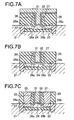
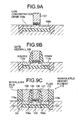
- Figs. 5A to 5C and Figs. 7A to 7C are cross-sectional structural views for explaining the process of manufacturing the nonvolatile memory element 20.
- the process of manufacturing the nonvolatile memory element 20 is mainly comprised of a tunnel oxide film forming step of forming the tunnel oxide film 24 on a Si substrate 21 which is a semiconductor substrate to be a base; a dummy gate electrode forming step of forming a dummy gate electrode 25 on the tunnel oxide film 24; a dummy gate electrode etching step of etching the dummy gate electrode 25; a low concentration drain forming step of forming the low concentration drains 26a and 26b; a gate sidewall forming step of covering a side of the dummy gate electrode 25 with the gate sidewall 27; a source and drain forming step of forming the source 28a and the drain 28b; an interlayer film forming step of forming the interlayer film 29; a dummy gate electrode removing step of removing the dummy gate electrode 25; a floating gate electrode forming step of forming the floating gate electrode 30 having an irregular shape on its own surface; an interlayer dielectric forming step of forming the interlayer dielectric 31 on
- the element isolation layer 22 is formed at the Si substrate 21 by means of shallow trench isolation and the like, then the embedded layer 23 for adjusting a threshold voltage is formed by means of a conventional ion implantation process.
- the Si substrate 21 is thermally oxidized at about 800°C for about 15 minutes so that, as shown in Fig. 5B, the tunnel oxide film 24 of about 8 nm is formed at a surface of the Si substrate 21 (the tunnel oxide film forming step).
- the tunnel oxide film forming step Using a conventional process such as LP-CVD process, a polycrystalline Si film is deposited up to about 600 nm so as to form the dummy gate electrode 25 (the dummy gate electrode forming step).
- the resulting layered structure is processed by means of a conventional lithographic technology and a conventional RIE technology so that a pattern of the dummy gate electrode 25 as shown in Fig. 5C is formed (the dummy gate electrode etching step).
- impurities such as phosphorus, arsenic, etc. are implanted by an ion implantation process at a concentration of 5 ⁇ 10 13 /cm 2 , for example, so as to form the low concentration drains 26a and 26b (the low concentration drain forming step).
- the gate sidewalls 27 are formed by means of conventional CVD and etch back processes (the gate sidewall forming step). Using the gate sidewalls 27 as masks, impurities such as phosphorus, arsenic, etc. are implanted by an ion implantation process at a concentration of 5 ⁇ 10 15 /cm 2 , for example, so as to form the source 28a and the drain 28b (the source and drain forming step).
- heat treatment at about 900°C for about 30 minutes by means of a conventional electric heating furnace or heat treatment at about 1050°C for 10 seconds by means of rapid thermal processing (RTP) is carried out to deposit the interlayer film 29 of Si oxide film etc. as shown in Fig. 6B (the interlayer film forming step).
- a planarization technology such as a CMP for a conventional insulating film
- a surface of the interlayer film 29 is planarized and the dummy gate electrode 25 is exposed so that the dummy gate electrode 25 is removed by a conventional etching process (the dummy gate electrode removing step).
- polycrystalline Si or the like is deposited on a surface of the tunnel oxide film 24 and a side of the gate sidewall 27 by means of a chemical vapor deposition process which is carried out in a situation where oxygen is removed from an air-tight CVD apparatus, so that the floating gate electrode 30 having an irregular shape of a substantial semicircle (hemispherical polysicon: Hemispherical Grain) on its own surface as shown in Fig. 4B is formed (the floating gate electrode forming step).
- the formation of the floating gate electrode 30 is carried out along an inner sidewall of the gate sidewall 27 and an upper surface of the interlayer film 29.
- the formation of such hemispherical polysicon is carried out in such a manner that an amorphous silicon is deposited on the tunnel oxide film 24 at a temperature of about 550°C for about 40 minutes by means of a chemical vapor deposition process using silane (SiH 4 ) within a CVD apparatus which is applicable to a ultra-high vacuum, for example so as to form an amorphous silicon film up to about 100 nm, then an annealing is carried out for about 10 minutes so as to grow hemispherical polysicon up to about 10 nm to 20 nm in grain diameter.
- the ultra even and highly reliable interlayer dielectric 31 of SiO 2 , Si 3 N 4 or the like is deposited up to about 15 nm along a surface (an inner surface of a sidewall) of the floating gate electrode 30 by means of an atomic layer chemical vapor deposition process at about 400°C (the interlayer dielectric forming step).
- a polycrystalline Si doped with phosphorus and the like is deposited on its surface so as to form the control electrode 32 (the control electrode forming step).
- the formation of SiO 2 layer out of the interlayer dielectric 31 may not be carried out by an atomic layer chemical vapor deposition process but may be carried out in a manner that after the hemispherical polysicon of the floating gate electrode 30 are thermally oxidized, Si 3 N 4 is deposited on a surface thereof by an atomic layer chemical vapor deposition process, for example, then the Si 3 N 4 is oxidized again.
- Fig. 7B these are planarized; the floating gate electrode 30 except for a gate portion, the interlayer dielectric 31, and the control electrode 32 are removed (the planarization step); and finally, as shown in Fig. 7C the plug 33, of a polycrystalline Si etc., to be a connecting portion of the source 28a and the drain 28b is formed (the plug forming step).
- the nonvolatile memory element 20 is configured in such a manner that the floating gate electrode 30 and the interlayer dielectric 31 surround a bottom surface and sides of the control electrode 32, the static capacity between the control electrode 32 and the floating gate electrode 30 can be larger than that of the first embodiment.
- the floating gate electrode 30 is formed to surround the bottom surface and the sides of the control electrode 32, so as to configure the nonvolatile memory element 20, a ratio (a coupling ratio) of a static capacity between the control electrode 32 and the floating gate electrode 30 to the whole static capacity of the floating gate electrode 30 can be significantly increased, and an applied voltage between the Si substrate 21 and the floating gate electrode 30 can be increased without increasing an applied voltage to the whole nonvolatile memory element 20, thereby enabling the applied voltage to the whole nonvolatile memory element 20 to be reduced.
- a drain withstanding voltage required for the drain can be decreased so that it becomes possible to miniaturize the element.
- nonvolatile memory element 20 is configured to be an FG type, sufficient density of storing charge, data retention time and endurance characteristics of write/erase may also be obtained.
- an FG type nonvolatile memory element of a conventional configuration provides a coupling ratio of about 0.36
- the nonvolatile memory element 20 according to the present embodiment provides a coupling ratio of about 0.9, thereby increasing the coupling ratio up to almost 2.5 times. Therefore, when a required write voltage for the nonvolatile memory element of the conventional configuration is about 20 V, a write voltage of about 8.7 V can be utilized for writing in the present embodiment.
- the present invention is not limited to the embodiments as described above.
- the interlayer dielectric may be formed by means of any manufacturing process other than such an atomic layer chemical vapor deposition process as far as it can form an ultra thin layer in a substantially conformal manner.
- the FG type nonvolatile memory element is configured by forming the tunnel oxide film on the Si substrate which is a semiconductor substrate to be a base; forming the floating gate electrode on the tunnel oxide film to have an irregular shape on its own surface; forming the highly even interlayer dielectric on the floating gate electrode having the irregular shape; and forming the control electrode on the interlayer dielectric, thereby maintaining sufficient density of stored charges, data retention time, and endurance characteristics of write/erase, and at the same time enabling a write voltage to decrease and the element itself to be miniaturized.
Landscapes
- Non-Volatile Memory (AREA)
- Semiconductor Memories (AREA)
Abstract
While maintaining sufficient density of stored charges, data retention time, and endurance characteristics of write/erase in a nonvolatile memory element, a write voltage may be decreased and the element itself may be miniaturized. A nonvolatile memory element (1) is configured by forming a tunnel oxide film (5) on a Si substrate (2) to be a base; forming, on the tunnel oxide film (5), a floating gate electrode (6) having a hemisphere polysicon on its own surface; forming a highly even interlayer dielectric (7) on the floating gate electrode (6) having an irregular shape; and forming a control electrode (8) on the interlayer dielectric (7). <IMAGE>
Description
The present invention relates to a nonvolatile
memory element retaining data regardless of whether its
power supply is on or off and a method of manufacturing
the nonvolatile memory element, and in particular to a
nonvolatile memory element configured to be of FG type
and a method of manufacturing the nonvolatile memory
element.
As for MIS (Metal Insulated Semiconductor) type
LSI's, many nonvolatile memory elements capable of
retaining data regardless of whether power supplies
thereof are on or off have been used as memory elements
to retain data. Examples of such nonvolatile memory
elements are typically an FG (Floating Gate) type
nonvolatile memory element and a MONOS (Metal - Si oxide
film - Si nitride film - Si substrate) type nonvolatile
memory element. Both elements charge to store
information in a given method.
At first, a process of manufacturing an FG type
nonvolatile memory element of a conventional design will
be described hereafter.
Such an FG type nonvolatile memory element is
configured to provide a floating gate electrode of
polycrystalline Si, for example, in an intermediate
position within a gate insulating film of an MIS type
transistor. By charging the floating gate electrode, a
threshold of the MIS type transistor is changed so as to
store information.
Figs. 8A to 8D and Figs. 9A to 9C are cross-sectional
views for explaining a process of manufacturing
an FG type nonvolatile memory element 100 of a
conventional design.
When manufacturing the FG type nonvolatile memory
element 100, firstly, as shown in Fig. 8A, an element
isolation layer 102 is formed in a Si substrate 101 by
means of shallow trench isolation and the like, then an
embedded layer 103 for adjusting a threshold voltage is
formed by means of a conventional ion implantation
process.
Next, the Si substrate 101 is thermally oxidized at
about 800°C for about 15 minutes so that, as shown in Fig.
8B, a tunnel oxide film 104 having a thickness of about 8
nm is formed on a surface of the Si substrate 101. Then,
a floating gate electrode 105 is formed on a surface
thereof to have a thickness of about 6 nm, further an
interlayer dielectric 106 is formed on a surface thereof.
Fig. 8C is an enlarged view showing a detailed
construction of the tunnel oxide film 104, the floating
gate electrode 105 and the interlayer dielectric 106
which are configured as described above. As shown in Fig.
8C, the interlayer dielectric 106 has a three-layer
construction of a Si oxide film 106a, a Si nitride film
106b and a Si oxide film 106c. The Si oxide film 106a is
formed by performing thermal oxidation on a surface of
the floating gate electrode 105 at about 850°C for about
10 minutes so as to have a thickness of about 5 nm. The
Si nitride film 106b is formed by conventional processes
such as an LP-CVD, plasma CVD on a surface of the Si
oxide film 106a such that the Si nitride film 106b may be
deposited up to about 12 nm. The Si oxide film 106c is
formed by thermal oxidation of a surface of the Si
nitride film 106b so as to have a thickness of about 6 nm.
After formation of the interlayer dielectric 106, as
shown in Fig. 8D, a control electrode 107 is formed of
polycrystalline Si, WSi, etc. including a high
concentration of phosphorus and the like, then patterned
by means of a conventional lithographic technology and an
RIE technology so as to be the control electrode 107 as
shown in Fig. 9A. Further, using the patterned control
electrode 107 as a mask, impurities such as phosphorus,
arsenic, etc. are implanted by an ion implantation
process at a concentration of 5 × 10¹³ /cm2, for example,
so as to form low concentration drains 108a and 108b.
Then, as shown in Fig. 9B, gate sidewalls 109 are
formed by means of conventional CVD and etch back
processes. Using the gate sidewalls 109 as masks,
impurities such as phosphorus, arsenic, etc. are
implanted by an ion implantation process at a
concentration of 5 × 10¹⁵ /cm2, for example, so as to form
a source 110a and a drain 110b.
Finally, in order to activate the implanted
impurities, heat treatment at about 900°C for about 30
minutes by means of a conventional electric heating
furnace or heat treatment at about 1050°C for 10 seconds
by means of rapid thermal processing (RTP) is carried out
to form an interlayer film 111 of Si oxide film etc. and
a plug 112 of W or polycrystalline Si to thereby
construct the nonvolatile memory element 100 as shown in
Fig. 9C.
As to the nonvolatile memory element 100, a voltage
of about + 20 V is applied to the control electrode 107
in a situation where the Si substrate 101 is grounded so
that, through a conduction channel area of the Si
substrate 101, charges are injected into and stored in
the floating gate electrode 105 by employing FN tunnel
current or the like. In the state of the stored charges,
a threshold voltage of the MIS type transistor is high.
The state of the stored charges is maintained even after
the voltage application to the control electrode 107 has
been stopped. Thus, the nonvolatile memory element 100
can retain data regardless of whether power supply for
the element is on or off.
Next, a manufacturing process of a MONOS type
nonvolatile memory element, of a conventional design,
will be described.
The MONOS type nonvolatile memory element has layers
comprised of metal- Si oxide film - Si nitride film - Si
oxide film - Si substrate. Charges are stored in
discrete traps which are in the Si nitride film and near
the boundary of the Si oxide film and the Si nitride film
so as to change threshold values of transistors and to
retain data (IE3 Trans, Electron Dev. ED39(2), 122(1983)).
Figs. 10A to 10C and Figs. 11A to 11C are cross-sectional
views for explaining a process of manufacturing
a MONOS type nonvolatile memory element 200.
When manufacturing the MONOS type nonvolatile memory
element 200, firstly, as shown in Fig. 10A, an element
isolation layer 202 is formed in a Si substrate 201 by
means of shallow trench isolation and the like, then an
embedded layer 203 for adjusting a threshold voltage is
formed by means of a conventional ion implantation
process.
Next, the Si substrate 201 is thermally oxidized at
about 800°C for about 15 minutes so that a tunnel oxide
film 204, about 3 nm thick, is formed on a surface of the
Si substrate 201. Then, a Si nitride film 205 is formed
on a surface thereof by means of conventional processes
such as an LP-CVD, a plasma CVD so as to have a thickness
of about 8 nm. Then, the Si nitride film 205 is oxidized
again in order to form a Si oxide film 206 of about 3 to
5 nm.
After formation of the Si oxide film 206, as shown
in Fig. 11A, a control electrode 207 is formed of
polycrystalline Si, WSi, etc. including a high
concentration of phosphorus and the like, then patterned
by means of conventional lithographic technology and RIE
technology so as to be the control electrode 207 as shown
in Fig. 11B.
Further, using the patterned control electrode 207
as a mask, impurities such as phosphorus, arsenic, etc.
are implanted by an ion implantation process at a
concentration of 5 × 10¹³ /cm2, for example, so as to form
low concentration drains 208a and 208b as shown in Fig.
11C.
Then, gate sidewalls 209 are formed by means of
conventional CVD and etch back processes. Using the gate
sidewalls 209 as masks, impurities such as phosphorus,
arsenic, etc. are implanted by an ion implantation
process at a concentration of 5 × 10¹⁵ /cm2, for example,
so as to form a source 210a and a drain 210b.
Finally, in order to activate the implanted
impurities, heat treatment at about 900°C for about 30
minutes by means of a conventional electric heating
furnace or heat treatment at about 1050°C for 10 seconds
by means of rapid thermal processing (RTP) is carried out
to form an interlayer film 211 of Si oxide film etc. and
a plug 212 of W or polycrystalline Si to thereby
construct the nonvolatile memory element 200.
As to the nonvolatile memory element 200 as formed
in the manner described above, traps to store charges are
formed in the Si nitride film 205 itself and in a SiON
transition layer located near the boundary of the Si
oxide film 206 and the Si nitride film 205; the charges
are discretely stored in the traps so as to retain data
regardless of whether power supply for the element is on
or off.
In the conventional FG type nonvolatile memory
element 100, however, if a leakage between the floating
gate electrode 105 and the Si substrate 101 occurs, all
charges stored at the floating gate electrode 105 are
lost, so that it is very difficult to make the tunnel
oxide film 104 thin. Thus, a problem arises in that,
when injecting charges from the channel area of the Si
substrate 101 to the floating gate electrode 105, a
required applying voltage between the Si substrate 101
and the floating gate electrode 105 should be increased,
and a data write voltage to be applied to the whole
nonvolatile memory element 100 should be also increased.
Still another problem arises in that when the data
write voltage is increased, in order to ensure a
sufficient withstanding voltage of the drain 110b, it may
be hard to make the drain 110b fine, and the nonvolatile
memory element 100 may not be miniaturized.
Further, since the MONOS type nonvolatile memory
element 200 discretely stores charges in traps which are
in the tunnel oxide film 204 and the SiON transition
layer near the boundary between the Si oxide film 206 and
Si nitride film 205 so as to retain data, a partial
leakage at the tunnel oxide film 204 does not lose all
the charges stored in the traps. Therefore, the tunnel
oxide film 204 may have a small thickness so that a data
write voltage may be reduced and the element may be
miniaturized compared with the FG type nonvolatile memory
element 100.
However, a trap density of the MONOS type
nonvolatile memory element 200 is not sufficiently high.
A density of charges to be stored is lower, by about five
digits, than that of the FG type nonvolatile memory
element 100.
Further, with respect to the MONOS nonvolatile
memory element 200, it is not easy to form its traps to
allow a good reproducibility of the density and a good
controllability. There may be introduced a problem that
the nonvolatile memory element 200 of a fine structure
does not provide sufficient data retention time or
sufficient endurance characteristics of write/erase.
In view of the above problems, the present invention
has been made so as to provide a nonvolatile memory
element which ensures sufficient density of stored
charges, data retention time, and endurance
characteristics of write/erase, and at the same time
enables a write voltage to decrease and the element
itself to be smaller, and to provide a method of
manufacturing the nonvolatile memory element.
In order to solve the problems as described above,
the present invention provides, in a nonvolatile memory
element which retains data regardless of whether power
supply for the element is on or off, the nonvolatile
memory element characterized by comprising a
semiconductor substrate to be a base; a tunnel oxide film
formed on the semiconductor substrate; a floating gate
electrode formed on the tunnel oxide film so as to have
an irregular shape on its own surface; an interlayer
dielectric formed on the floating gate electrode; and a
control electrode formed on the interlayer dielectric.
In the nonvolatile memory element, the surface of
the floating gate electrode is formed to have the
irregular shape so that a surface area of the floating
gate electrode is larger, whereby a static capacity
between the control electrode and the floating gate
electrode can be increased. Thus, a ratio (a coupling
ratio) of the static capacity between the control
electrode and the floating gate electrode to the whole
static capacity of the floating gate electrode can be
increased so that an applied voltage between the
semiconductor substrate and the floating gate electrode
can be increased without increasing a voltage applied to
the whole nonvolatile memory element.
Further, in the nonvolatile memory element according
to the present invention, the irregular shape of the
floating gate electrode may preferably be in an irregular
shape on a substantially hemisphere.
Furthermore, in the nonvolatile memory element
according to the present invention, the irregular shape
of the floating gate electrode is preferably formed so
that a grain size may be 10 nm to 20 nm.
Still further, in the nonvolatile memory element
according to the present invention, the interlayer
dielectric is preferably formed by means of an atomic
layer chemical vapor deposition process.
Further, in the nonvolatile memory element according
to the present invention, the floating gate electrode and
the interlayer dielectric are preferably formed so as to
surround a bottom surface and sidewalls of the control
electrode.
The nonvolatile memory element according to the
present invention is preferably for a flash memory.
In addition, there is provided, in a method of
manufacturing a nonvolatile memory element which retains
data regardless of whether power supply for the element
is on or off, the method characterized by comprising a
tunnel oxide film forming step of forming a tunnel oxide
film on a Si substrate to be a base; a floating gate
electrode forming step of forming, on the tunnel oxide
film, a floating gate electrode having a surface of an
irregular shape; an interlayer dielectric forming step of
forming an interlayer dielectric on the floating gate
electrode; a control electrode forming step of forming a
control electrode on the interlayer dielectric.
Herein, the surface of the floating gate electrode
is formed in the irregular shape so that a surface area
of the floating gate electrode is larger, whereby a
static capacity between the control electrode and the
floating gate electrode can be increased. Thus, a ratio
(a coupling ratio) of the static capacity between the
control electrode and the floating gate electrode to the
whole static capacity of the floating gate electrode can
be increased so that an applied voltage between the
semiconductor substrate and the floating gate electrode
can be increased without increasing a voltage applied to
the whole nonvolatile memory element.
Further, in the method of manufacturing the
nonvolatile memory element according to the present
invention, the interlayer dielectric is preferably formed
by means of an atomic layer chemical vapor deposition
process in the interlayer dielectric forming step.
The method of manufacturing the nonvolatile memory
element according to the present invention preferably
further comprises, in order to form a gate electrode, a
gate electrode etching step of etching the tunnel oxide
film, the floating gate electrode, the interlayer
dielectric and the control electrode respectively formed
by the tunnel oxide film forming step, the floating gate
electrode forming step, the interlayer dielectric forming
step and the control electrode forming step.
Further, the method of manufacturing the nonvolatile
memory element according to the present invention
preferably further comprises a dummy gate electrode
forming step of forming a dummy gate electrode on the
tunnel oxide film subsequent to the tunnel oxide film
forming step; a dummy gate electrode etching step of
etching the dummy gate electrode; a gate sidewall forming
step of covering a sidewall of the dummy gate electrode
with a gate sidewall; a dummy gate electrode removing
step of removing the dummy gate electrode subsequent to
forming the gate sidewall. In the floating gate
electrode forming step, the floating gate electrode is
formed along an inner sidewall of the gate sidewall. In
the interlayer dielectric forming step, the interlayer
dielectric is formed along an inner sidewall of the
floating gate electrode.
With reference to the drawings, embodiments of the
present invention will be described hereafter.
Firstly, a first embodiment according to the present
invention will be described.
Figs. 1A to 1B are structural views showing a
structure of a nonvolatile memory element 1. Fig. 1A
shows a cross-sectional view of the nonvolatile memory
element 1, and Fig. 1B shows an enlarged cross-sectional
view of a portion A in Fig. 1A.
The nonvolatile memory element 1 is an FG type
nonvolatile memory element which is utilized as a flash
memory, for example, and is mainly comprised of a Si
substrate 2 which is a semiconductor substrate to be a
base; an element isolation layer 3; an embedded layer 4
provided in the Si substrate 2 so as to adjust a
threshold voltage; a tunnel oxide film 5 formed on the Si
substrate 2; a floating gate electrode 6 formed on the
tunnel oxide film 5 so as to have an irregular shape on
its own surface; an interlayer dielectric 7 formed on the
floating gate electrode 6; a control electrode 8 provided
on the interlayer dielectric 7; low concentration drains
9a and 9b formed at a surface of the Si substrate 2; a
source 11a; a drain 11b; a gate sidewall 10 formed on an
upper surface of the Si substrate 2; an interlayer film
12; and a plug 13.
As shown in Fig. 1B, the floating gate electrode 6
of the nonvolatile memory element 1 is formed to have the
irregular shape on its own surface so that a surface area
of the floating gate electrode 6 is increased and a
static capacity between the floating gate electrode 6 and
the control electrode 8 can be increased. The irregular
shape may be of a substantial hemisphere such as a
mushroom shape, a waveform, or any other rugged shape,
however, the surface area of the resulting floating gate
electrode 6 preferably has constant accuracy.
Next, a process of manufacturing the nonvolatile
memory element 1 will be described.
Figs. 2A to 2C and Figs. 3A to 3C are cross-sectional
structural views for explaining the process of
manufacturing the nonvolatile memory element 1.
The process of manufacturing the nonvolatile memory
element 1 is mainly comprised of a tunnel oxide film
forming step of forming the tunnel oxide film 5 on the Si
substrate 2 which is a semiconductor substrate to be a
base; a floating gate electrode forming step of forming,
on the tunnel oxide film 5, the floating gate electrode 6
having an irregular shape on its own surface; an
interlayer dielectric forming step of forming the
interlayer dielectric 7 on the floating gate electrode 6;
a control electrode forming step of forming the control
electrode 8 on the interlayer dielectric 7; a gate
electrode etching step of etching, in order to form a
gate electrode, the tunnel oxide film 5, the floating
gate electrode 6, the interlayer dielectric 7 and the
control electrode 8; a low concentration drain forming
step of forming the low concentration drains 9a and 9b; a
gate sidewall forming step of forming the gate sidewall
10; a source and drain forming step of forming the source
11a and the drain 11b; an interlayer film forming step of
forming the interlayer film 12; and a plug forming step
of the plug 13.
Each step will be described hereafter.
When manufacturing the nonvolatile memory element 1,
firstly, as shown in Fig. 2A, the element isolation layer
3 is formed in the Si substrate 2 by means of shallow
trench isolation and the like, then the embedded layer 4
for adjusting a threshold voltage is formed by means of a
conventional ion implantation process.
Next, the Si substrate 2 is thermally oxidized at
about 800°C for about 15 minutes so that, as shown in Fig.
2B, the tunnel oxide film 5 having a thickness of about 8
nm is formed on a surface of the Si substrate 2 (the
tunnel oxide film forming step). Then, polycrystalline
Si or the like is deposited on the tunnel oxide film 5 by
means of a chemical vapor deposition (CVD) process which
is carried out in a situation where oxygen is removed
from an air-tight CVD apparatus, so that the floating
gate electrode 6 having an irregular shape of a
substantial hemisphere (hemispherical polysicon:
Hemispherical Grain) on its own surface as shown in Fig.
1B is formed (the floating gate electrode forming step).
To form such hemispherical polysicon, an amorphous
silicon is deposited on a surface of the tunnel oxide
film 5 at a temperature of about 550°C for about 40
minutes by means of a chemical vapor deposition (CVD)
process using silane (SiH4) within a CVD apparatus which
is applicable to a ultra-high vacuum, for example, so
that an amorphous silicon film of about 100 nm is formed.
Further, an annealing is carried out for about 10 minutes
so as to grow hemispherical polysicon up to about 10 nm
to 20 nm in grain diameter.
After formation of the floating gate electrode 6,
the highly reliable interlayer dielectric 7 of SiO2, Si3N4
or the like is grown on a surface of the floating gate
electrode 6 up to about 15 nm by means of a film forming
process to provide an ultra thin and ultra even film,
such as an atomic layer chemical vapor deposition (AL-CVD)
process (the interlayer dielectric forming step).
Notably, the interlayer dielectric 7 formed in this step
is preferably configured to have an even thickness to
cover the hemisphere polysicon of the floating gate
electrode 6.
After formation of the interlayer dielectric 7, a
polycrystalline Si, a WSi or the like having a high
concentration of phosphorus and the like is deposited on
a surface of the interlayer dielectric 7 by means of a
conventional LP-CVD and the like so as to form the
control electrode 8 as shown in Fig. 2C (the control
electrode forming step). Then, patterning of the control
electrode 8 as shown in Fig. 3A is carried out by means
of conventional lithographic technology and RIE
technology (the gate electrode etching step). By this
gate electrode etching step, the tunnel oxide film 5, the
floating gate electrode 6, the interlayer dielectric 7
and the control electrode 8 which are respectively formed
by the tunnel oxide film forming step, the floating gate
electrode forming step, the interlayer dielectric forming
step and the control electrode forming step are etched so
as to form the gate electrode.
Using the patterned control electrode 8 as a mask,
impurities such as phosphorus, arsenic, etc. are
implanted by an ion implantation process at a
concentration of 5 × 10¹³ /cm2, for example, so as to form
the low concentration drains 9a and 9b (the low
concentration drain forming step).
Then, as shown in Fig. 3B, the gate sidewalls 10 are
formed by means of conventional CVD and etch back
processes (the gate sidewall forming step). Using the
gate sidewalls 10 as masks, impurities such as phosphorus,
arsenic, etc. are implanted by an ion implantation
process at a concentration of 5 × 10¹⁵ /cm2, for example.
so as to form a source 11a and a drain 11b (the source
and drain forming step).
Finally, in order to activate the implanted
impurities, heat treatment at about 900°C for about 30
minutes by means of a conventional electric heating
furnace or heat treatment at about 1050°C for 10 seconds
by means of rapid thermal processing (RTP) is carried out
to form the interlayer film 12 of Si oxide film to be a
connecting portion of the source 11a or the drain 11b
(the interlayer film forming step); and the plug 13 of W
or polycrystalline Si is formed (the plug forming step),
thereby constructing the nonvolatile memory element 1 as
shown in Fig. 3C.
As described above, the nonvolatile memory element 1
is configured to have the floating gate electrode 6 where
the hemisphere polysicon is formed on its surface and the
interlayer dielectric 7 formed on the hemisphere
polysicon to be highly even, so that the surface area of
the floating gate electrode 6 is larger, to thereby
increase the static capacity between the control
electrode 8 and the floating gate electrode 6. Thus, a
ratio (a coupling ratio) of the static capacity between
the control electrode 8 and the floating gate electrode 6
to the whole static capacity of the floating gate
electrode 6 can be increased so that an applied voltage
between the Si substrate 2 and the floating gate
electrode 6 can be increased without increasing a write
voltage to the whole nonvolatile memory element 1.
As described above, in the embodiment, the
nonvolatile memory element 1 is configured by forming the
tunnel oxide film 5 on the Si substrate 2 to be a base;
forming the floating gate electrode 6 on the tunnel oxide
film 5 to have hemisphere polysicon on its own surface;
forming the highly even interlayer dielectric 7 on the
floating gate electrode 6; and forming the control
electrode 8 on the interlayer dielectric 7, so that the
coupling ratio is increased, whereby the applied voltage
between the Si substrate 2 and the floating gate
electrode 6 can be increased without increasing the write
voltage to the whole nonvolatile memory element 1.
Therefore, it becomes possible to decrease the write
voltage for the nonvolatile memory element 1, and further,
it becomes possible to decrease a withstanding voltage
required for the drain, so that the element can be
miniaturized. Further, since the nonvolatile memory
element 1 is configured to be an FG type, sufficient
density of storing charge, data retention time and
endurance characteristics of write/erase may also be
obtained.
Next, a second embodiment according to the present
invention will be described.
The present embodiment is an application to the
first embodiment and is different from the first
embodiment in a configuration of a floating gate
electrode 30 and an interlayer dielectric 31.
Figs. 4A to 4B are structural views showing a
structure of a nonvolatile memory element 20 according to
the present embodiment. Fig. 4A shows a cross-sectional
view of the nonvolatile memory element 20, and Fig. 4B
shows an enlarged cross-sectional view of a portion B in
Fig. 4A.
The nonvolatile memory element 20 is an FG type
nonvolatile memory element which is utilized as a flash
memory, for example, and is mainly comprised of a Si
substrate 21 which is a semiconductor substrate to be a
base; an element isolation layer 22; an embedded layer 23
provided in the Si substrate 21 so as to adjust a
threshold voltage; a tunnel oxide film 24 formed on the
Si substrate 21; a floating gate electrode 30 formed on
the tunnel oxide film 24 so as to have an irregular shape
on its own surface; an interlayer dielectric 31 formed on
the floating gate electrode 30; a control electrode 32
provided on the interlayer dielectric 31; low
concentration drains 26a and 26b formed at a surface of
the Si substrate 21; a source 28a; a drain 28b; a gate
sidewall 27 formed on an upper surface of the Si
substrate 21; an interlayer film 29; and a plug 33.
Herein, the floating gate electrode 30 and the
interlayer dielectric 31 are formed so as to surround a
bottom surface and sidewalls of the control electrode 32,
which are different from the first embodiment. Thus,
comparing with the first embodiment, it becomes possible
to increase a ratio (a coupling ratio) of a static
capacity between the control electrode 32 and the
floating gate electrode 30 to the whole static capacity
of the floating gate electrode 30.
As shown in Fig. 4B, the floating gate electrode 30
of the nonvolatile memory element 20 is formed to have
the irregular shape on its own surface so that a surface
area of the floating gate electrode 30 can be increased
and a static capacity between the floating gate electrode
30 and the control electrode 32 can be increased. The
irregular shape may be of a substantial hemisphere such
as a mushroom shape, a waveform, or any other rugged
shape, however, the surface area of the resulting
floating gate electrode 30 preferably has constant
accuracy.
Then, a process of manufacturing the nonvolatile
memory element 20 will be described.
Figs. 5A to 5C and Figs. 7A to 7C are cross-sectional
structural views for explaining the process of
manufacturing the nonvolatile memory element 20.
The process of manufacturing the nonvolatile memory
element 20 is mainly comprised of a tunnel oxide film
forming step of forming the tunnel oxide film 24 on a Si
substrate 21 which is a semiconductor substrate to be a
base; a dummy gate electrode forming step of forming a
dummy gate electrode 25 on the tunnel oxide film 24; a
dummy gate electrode etching step of etching the dummy
gate electrode 25; a low concentration drain forming step
of forming the low concentration drains 26a and 26b; a
gate sidewall forming step of covering a side of the
dummy gate electrode 25 with the gate sidewall 27; a
source and drain forming step of forming the source 28a
and the drain 28b; an interlayer film forming step of
forming the interlayer film 29; a dummy gate electrode
removing step of removing the dummy gate electrode 25; a
floating gate electrode forming step of forming the
floating gate electrode 30 having an irregular shape on
its own surface; an interlayer dielectric forming step of
forming the interlayer dielectric 31 on the floating gate
electrode 30; a control electrode forming step of forming
the control electrode 32 on the interlayer dielectric 31;
a planarization step of removing the floating gate
electrode 30 except for a gate portion, the interlayer
dielectric 31, and the control electrode 32; and a plug
forming step of forming the plug 33.
Each step will be described hereafter.
When manufacturing the nonvolatile memory element 20,
firstly, as shown in Fig. 5A, the element isolation layer
22 is formed at the Si substrate 21 by means of shallow
trench isolation and the like, then the embedded layer 23
for adjusting a threshold voltage is formed by means of a
conventional ion implantation process.
Next, the Si substrate 21 is thermally oxidized at
about 800°C for about 15 minutes so that, as shown in Fig.
5B, the tunnel oxide film 24 of about 8 nm is formed at a
surface of the Si substrate 21 (the tunnel oxide film
forming step). Using a conventional process such as LP-CVD
process, a polycrystalline Si film is deposited up to
about 600 nm so as to form the dummy gate electrode 25
(the dummy gate electrode forming step).
Then, the resulting layered structure is processed
by means of a conventional lithographic technology and a
conventional RIE technology so that a pattern of the
dummy gate electrode 25 as shown in Fig. 5C is formed
(the dummy gate electrode etching step). After
patterning of the dummy gate electrode 25, using the
dummy gate electrode 25 as masks, impurities such as
phosphorus, arsenic, etc. are implanted by an ion
implantation process at a concentration of 5 × 10¹³/cm2,
for example, so as to form the low concentration drains
26a and 26b (the low concentration drain forming step).
Then, as shown in Fig. 6A, the gate sidewalls 27 are
formed by means of conventional CVD and etch back
processes (the gate sidewall forming step). Using the
gate sidewalls 27 as masks, impurities such as phosphorus,
arsenic, etc. are implanted by an ion implantation
process at a concentration of 5 × 10¹⁵ /cm2, for example,
so as to form the source 28a and the drain 28b (the
source and drain forming step).
In order to activate the implanted impurities, heat
treatment at about 900°C for about 30 minutes by means of
a conventional electric heating furnace or heat treatment
at about 1050°C for 10 seconds by means of rapid thermal
processing (RTP) is carried out to deposit the interlayer
film 29 of Si oxide film etc. as shown in Fig. 6B (the
interlayer film forming step).
Then, as shown in Fig. 6C, by using a planarization
technology such as a CMP for a conventional insulating
film, a surface of the interlayer film 29 is planarized
and the dummy gate electrode 25 is exposed so that the
dummy gate electrode 25 is removed by a conventional
etching process (the dummy gate electrode removing step).
Subsequently, as shown in Fig. 7A, polycrystalline
Si or the like is deposited on a surface of the tunnel
oxide film 24 and a side of the gate sidewall 27 by means
of a chemical vapor deposition process which is carried
out in a situation where oxygen is removed from an air-tight
CVD apparatus, so that the floating gate electrode
30 having an irregular shape of a substantial semicircle
(hemispherical polysicon: Hemispherical Grain) on its own
surface as shown in Fig. 4B is formed (the floating gate
electrode forming step).
The formation of the floating gate electrode 30 is
carried out along an inner sidewall of the gate sidewall
27 and an upper surface of the interlayer film 29. The
formation of such hemispherical polysicon is carried out
in such a manner that an amorphous silicon is deposited
on the tunnel oxide film 24 at a temperature of about
550°C for about 40 minutes by means of a chemical vapor
deposition process using silane (SiH4) within a CVD
apparatus which is applicable to a ultra-high vacuum, for
example so as to form an amorphous silicon film up to
about 100 nm, then an annealing is carried out for about
10 minutes so as to grow hemispherical polysicon up to
about 10 nm to 20 nm in grain diameter.
After formation of the floating gate electrode 30,
the ultra even and highly reliable interlayer dielectric
31 of SiO2, Si3N4 or the like is deposited up to about 15
nm along a surface (an inner surface of a sidewall) of
the floating gate electrode 30 by means of an atomic
layer chemical vapor deposition process at about 400°C
(the interlayer dielectric forming step). A
polycrystalline Si doped with phosphorus and the like is
deposited on its surface so as to form the control
electrode 32 (the control electrode forming step).
Notably, the formation of SiO2 layer out of the
interlayer dielectric 31 may not be carried out by an
atomic layer chemical vapor deposition process but may be
carried out in a manner that after the hemispherical
polysicon of the floating gate electrode 30 are thermally
oxidized, Si3N4 is deposited on a surface thereof by an
atomic layer chemical vapor deposition process, for
example, then the Si3N4 is oxidized again.
Subsequently, as shown in Fig. 7B, these are
planarized; the floating gate electrode 30 except for a
gate portion, the interlayer dielectric 31, and the
control electrode 32 are removed (the planarization
step); and finally, as shown in Fig. 7C the plug 33, of a
polycrystalline Si etc., to be a connecting portion of
the source 28a and the drain 28b is formed (the plug
forming step).
As described above, since the nonvolatile memory
element 20 is configured in such a manner that the
floating gate electrode 30 and the interlayer dielectric
31 surround a bottom surface and sides of the control
electrode 32, the static capacity between the control
electrode 32 and the floating gate electrode 30 can be
larger than that of the first embodiment.
As described above, in the present embodiment, since
the floating gate electrode 30 is formed to surround the
bottom surface and the sides of the control electrode 32,
so as to configure the nonvolatile memory element 20, a
ratio (a coupling ratio) of a static capacity between the
control electrode 32 and the floating gate electrode 30
to the whole static capacity of the floating gate
electrode 30 can be significantly increased, and an
applied voltage between the Si substrate 21 and the
floating gate electrode 30 can be increased without
increasing an applied voltage to the whole nonvolatile
memory element 20, thereby enabling the applied voltage
to the whole nonvolatile memory element 20 to be reduced.
Further, a drain withstanding voltage required for
the drain can be decreased so that it becomes possible to
miniaturize the element.
Further, since the nonvolatile memory element 20 is
configured to be an FG type, sufficient density of
storing charge, data retention time and endurance
characteristics of write/erase may also be obtained.
As an example, when comparison is made in a typical
FG type nonvolatile memory element of the 0.18 µm
generation having a gate length of 0.18 µm, a gate width
of 1.0 µm, and a gate height of 0.6 µm, an FG type
nonvolatile memory element of a conventional
configuration provides a coupling ratio of about 0.36,
whereas the nonvolatile memory element 20 according to
the present embodiment provides a coupling ratio of about
0.9, thereby increasing the coupling ratio up to almost
2.5 times. Therefore, when a required write voltage for
the nonvolatile memory element of the conventional
configuration is about 20 V, a write voltage of about 8.7
V can be utilized for writing in the present embodiment.
It should be noted that the present invention is not
limited to the embodiments as described above. For
example, in the first and the second embodiments,
although the highly even interlayer dielectric is formed
on the surface of the floating gate electrode having
hemispherical polysicon by using an atomic layer chemical
vapor deposition process, the interlayer dielectric may
be formed by means of any manufacturing process other
than such an atomic layer chemical vapor deposition
process as far as it can form an ultra thin layer in a
substantially conformal manner.
As described above, according to the present
invention, the FG type nonvolatile memory element is
configured by forming the tunnel oxide film on the Si
substrate which is a semiconductor substrate to be a
base; forming the floating gate electrode on the tunnel
oxide film to have an irregular shape on its own surface;
forming the highly even interlayer dielectric on the
floating gate electrode having the irregular shape; and
forming the control electrode on the interlayer
dielectric, thereby maintaining sufficient density of
stored charges, data retention time, and endurance
characteristics of write/erase, and at the same time
enabling a write voltage to decrease and the element
itself to be miniaturized.
Claims (10)
- In a nonvolatile memory element which retains data regardless of whether power supply for the element is on or off, said nonvolatile memory element is characterized by comprising:a semiconductor substrate to be a base;a tunnel oxide film formed on said semiconductor substrate;a floating gate electrode formed on said tunnel oxide film so as to have an irregular shape on a surface thereof;an interlayer dielectric formed on said floating gate electrode; anda control electrode formed on said interlayer dielectric.
- The nonvolatile memory element according to claim 1, characterized in that said irregular shape is a substantially hemispherical shape.
- The nonvolatile memory element according to claim 2, characterized in that a grain diameter of said irregular shape ranges from 10 nm to 20 nm.
- The nonvolatile memory element according to claim 1, characterized in that said interlayer dielectric is formed by using an atomic layer chemical vapor deposition process.
- The nonvolatile memory element according to claim 1,
characterized in that said floating gate electrode and said interlayer dielectric are formed so as to surround a bottom surface and sides of said control electrode. - The nonvolatile memory element according to claim 1, characterized by being for a flash memory.
- In a method of manufacturing a nonvolatile memory element which retains data regardless of whether power supply for the element is on or off, said method of manufacturing a nonvolatile memory element is characterized by comprising:a tunnel oxide film forming step of forming a tunnel oxide film on a semiconductor substrate to be a base;a floating gate electrode forming step of forming, on the tunnel oxide film, a floating gate electrode having an irregular shape on a surface thereof;an interlayer dielectric forming step of forming an interlayer dielectric on the floating gate electrode; anda control electrode forming step of forming a control electrode on the interlayer dielectric.
- The method of manufacturing a nonvolatile memory element according to claim 7, characterized in that said interlayer dielectric forming step is carried out to form the interlayer dielectric by using an atomic layer chemical vapor deposition process.
- The method of manufacturing a nonvolatile memory element according to claim 7, characterized by further comprising:a gate electrode etching step of etching the tunnel oxide film, the floating gate electrode, the interlayer dielectric, and the control electrode which are formed by said tunnel oxide film forming step, said floating gate electrode forming step, said interlayer dielectric forming step, and said control electrode forming step so as to form a gate electrode.
- The method of manufacturing a nonvolatile memory element according to claim 7, characterized by further comprising:a dummy gate electrode forming step of forming a dummy gate electrode on the tunnel oxide film subsequent to said tunnel oxide film forming step;a dummy gate electrode etching step of etching the dummy gate electrode;a gate sidewall forming step of covering a sidewall of the dummy gate electrode with a gate sidewall; anda dummy gate electrode removing step of removing the dummy gate electrode subsequent to forming the gate sidewall, wherein said floating gate electrode forming step is carried out to form the floating gate electrode along an inner sidewall of the gate sidewall, and said interlayer dielectric forming step is carried out to form the interlayer dielectric along an inner sidewall of the floating gate electrode.
Applications Claiming Priority (3)
| Application Number | Priority Date | Filing Date | Title |
|---|---|---|---|
| JP2000362215A JP2002164448A (en) | 2000-11-29 | 2000-11-29 | Nonvolatile storage element and method of manufacturing nonvolatile storage element |
| JP2000362215 | 2000-11-29 | ||
| PCT/JP2001/010395 WO2002045175A1 (en) | 2000-11-29 | 2001-11-28 | Nonvolatile storage device and method for manufacturing nonvolatile storage device |
Publications (1)
| Publication Number | Publication Date |
|---|---|
| EP1267416A1 true EP1267416A1 (en) | 2002-12-18 |
Family
ID=18833531
Family Applications (1)
| Application Number | Title | Priority Date | Filing Date |
|---|---|---|---|
| EP01999009A Withdrawn EP1267416A1 (en) | 2000-11-29 | 2001-11-28 | Nonvolatile storage device and method for manufacturing nonvolatile storage device |
Country Status (6)
| Country | Link |
|---|---|
| US (1) | US20030003662A1 (en) |
| EP (1) | EP1267416A1 (en) |
| JP (1) | JP2002164448A (en) |
| KR (1) | KR20020074219A (en) |
| TW (1) | TW515090B (en) |
| WO (1) | WO2002045175A1 (en) |
Families Citing this family (10)
| Publication number | Priority date | Publication date | Assignee | Title |
|---|---|---|---|---|
| US6995414B2 (en) | 2001-11-16 | 2006-02-07 | Kabushiki Kaisha Toshiba | Semiconductor memory device including multi-layer gate structure |
| GB2395065B (en) * | 2002-10-30 | 2005-01-19 | Toumaz Technology Ltd | Floating gate transistors |
| KR100526479B1 (en) * | 2003-12-31 | 2005-11-08 | 동부아남반도체 주식회사 | Method for fabricating flash memory |
| JP4854955B2 (en) * | 2004-12-10 | 2012-01-18 | ルネサスエレクトロニクス株式会社 | Semiconductor device and manufacturing method thereof |
| US8022489B2 (en) * | 2005-05-20 | 2011-09-20 | Macronix International Co., Ltd. | Air tunnel floating gate memory cell |
| US20070105295A1 (en) * | 2005-11-08 | 2007-05-10 | Dongbuanam Semiconductor Inc. | Method for forming lightly-doped-drain metal-oxide-semiconductor (LDD MOS) device |
| JP2007251132A (en) * | 2006-02-16 | 2007-09-27 | Toshiba Corp | MONOS-type non-volatile memory cell, non-volatile memory and manufacturing method thereof |
| KR100751662B1 (en) | 2006-03-31 | 2007-08-23 | 주식회사 하이닉스반도체 | Manufacturing Method of Flash Memory Device |
| US20100163952A1 (en) * | 2008-12-31 | 2010-07-01 | Chia-Hong Jan | Flash Cell with Integrated High-K Dielectric and Metal-Based Control Gate |
| US20110133266A1 (en) * | 2009-12-03 | 2011-06-09 | Sanh Tang | Flash Memory Having a Floating Gate in the Shape of a Curved Section |
Family Cites Families (5)
| Publication number | Priority date | Publication date | Assignee | Title |
|---|---|---|---|---|
| JP3203709B2 (en) * | 1991-10-14 | 2001-08-27 | ソニー株式会社 | Semiconductor device having floating gate and method of manufacturing the same |
| JPH09205154A (en) * | 1996-01-25 | 1997-08-05 | Mitsubishi Electric Corp | Semiconductor device and manufacturing method thereof |
| JPH10189778A (en) * | 1996-12-26 | 1998-07-21 | Sony Corp | Semiconductor memory device and method of manufacturing the same |
| JPH11111865A (en) * | 1997-09-30 | 1999-04-23 | Hitachi Ltd | Semiconductor device and manufacturing method thereof |
| KR100275738B1 (en) * | 1998-08-07 | 2000-12-15 | 윤종용 | Method for producing thin film using atomatic layer deposition |
-
2000
- 2000-11-29 JP JP2000362215A patent/JP2002164448A/en active Pending
-
2001
- 2001-11-20 TW TW090128733A patent/TW515090B/en not_active IP Right Cessation
- 2001-11-28 US US10/182,407 patent/US20030003662A1/en not_active Abandoned
- 2001-11-28 WO PCT/JP2001/010395 patent/WO2002045175A1/en not_active Ceased
- 2001-11-28 EP EP01999009A patent/EP1267416A1/en not_active Withdrawn
- 2001-11-28 KR KR1020027009759A patent/KR20020074219A/en not_active Withdrawn
Non-Patent Citations (1)
| Title |
|---|
| See references of WO0245175A1 * |
Also Published As
| Publication number | Publication date |
|---|---|
| TW515090B (en) | 2002-12-21 |
| WO2002045175A1 (en) | 2002-06-06 |
| US20030003662A1 (en) | 2003-01-02 |
| JP2002164448A (en) | 2002-06-07 |
| KR20020074219A (en) | 2002-09-28 |
Similar Documents
| Publication | Publication Date | Title |
|---|---|---|
| JP3159850B2 (en) | Nonvolatile semiconductor memory device and method of manufacturing the same | |
| US20030075756A1 (en) | Nonvolatile semiconductor memory device and its manufacturing method | |
| US7652322B2 (en) | Split gate flash memory device having self-aligned control gate and method of manufacturing the same | |
| US8008153B2 (en) | Methods of fabricating nonvolatile memory devices having gate structures doped by nitrogen | |
| US6538277B2 (en) | Split-gate flash cell | |
| US7192830B2 (en) | Method for fabricating a memory cell | |
| US20100173488A1 (en) | Non-volatile memory with erase gate on isolation zones | |
| US6746920B1 (en) | Fabrication method of flash memory device with L-shaped floating gate | |
| US20040241942A1 (en) | Self-aligned structure with unique erasing gate in split gate flash | |
| US7179709B2 (en) | Method of fabricating non-volatile memory device having local SONOS gate structure | |
| US6362045B1 (en) | Method to form non-volatile memory cells | |
| EP1671367A1 (en) | 2-transistor memory cell and method for manufacturing | |
| US7601594B2 (en) | Method for fabricating semiconductor memory | |
| US6740557B1 (en) | Spacer like floating gate formation | |
| EP1267416A1 (en) | Nonvolatile storage device and method for manufacturing nonvolatile storage device | |
| KR20060035551A (en) | Nonvolatile Memory Device and Manufacturing Method Thereof | |
| US7064378B2 (en) | Local-length nitride SONOS device having self-aligned ONO structure and method of manufacturing the same | |
| US6180463B1 (en) | Method for fabricating a multi-level mask ROM | |
| US7148110B2 (en) | Local-length nitride SONOS device having self-aligned ONO structure and method of manufacturing the same | |
| US6127698A (en) | High density/speed nonvolatile memories with a textured tunnel oxide and a high capacitive-coupling ratio | |
| JP4590744B2 (en) | Nonvolatile semiconductor memory device and manufacturing method thereof | |
| US20070202646A1 (en) | Method for forming a flash memory floating gate | |
| JPH1126617A (en) | Manufacture of nonvolatile semiconductor memory |
Legal Events
| Date | Code | Title | Description |
|---|---|---|---|
| PUAI | Public reference made under article 153(3) epc to a published international application that has entered the european phase |
Free format text: ORIGINAL CODE: 0009012 |
|
| AK | Designated contracting states |
Kind code of ref document: A1 Designated state(s): AT BE CH CY DE DK ES FI FR GB GR IE IT LI LU MC NL PT SE TR |
|
| 17P | Request for examination filed |
Effective date: 20021107 |
|
| STAA | Information on the status of an ep patent application or granted ep patent |
Free format text: STATUS: THE APPLICATION HAS BEEN WITHDRAWN |
|
| 18W | Application withdrawn |
Effective date: 20040301 |
|
| RBV | Designated contracting states (corrected) |
Designated state(s): DE FR |