EP1267353A2 - Semiconductor integrated circuit device and data writing method therefor - Google Patents
Semiconductor integrated circuit device and data writing method therefor Download PDFInfo
- Publication number
- EP1267353A2 EP1267353A2 EP01129839A EP01129839A EP1267353A2 EP 1267353 A2 EP1267353 A2 EP 1267353A2 EP 01129839 A EP01129839 A EP 01129839A EP 01129839 A EP01129839 A EP 01129839A EP 1267353 A2 EP1267353 A2 EP 1267353A2
- Authority
- EP
- European Patent Office
- Prior art keywords
- bit line
- complimentary
- data
- line
- predetermined
- Prior art date
- Legal status (The legal status is an assumption and is not a legal conclusion. Google has not performed a legal analysis and makes no representation as to the accuracy of the status listed.)
- Withdrawn
Links
Images








Classifications
-
- G—PHYSICS
- G11—INFORMATION STORAGE
- G11C—STATIC STORES
- G11C7/00—Arrangements for writing information into, or reading information out from, a digital store
- G11C7/10—Input/output [I/O] data interface arrangements, e.g. I/O data control circuits, I/O data buffers
- G11C7/1078—Data input circuits, e.g. write amplifiers, data input buffers, data input registers, data input level conversion circuits
-
- G—PHYSICS
- G11—INFORMATION STORAGE
- G11C—STATIC STORES
- G11C7/00—Arrangements for writing information into, or reading information out from, a digital store
- G11C7/12—Bit line control circuits, e.g. drivers, boosters, pull-up circuits, pull-down circuits, precharging circuits, equalising circuits, for bit lines
Definitions
- the present invention relates to data writing into a memory cell in a semiconductor integrated circuit device. More particularly, the present invention relates to reduction of noise caused by a writing operation.
- FC RAM fast cycle random access memory
- a memory cell section 1000 shown in FIG. 20 is a specific example showing a configuration of a high speed memory. Required constituent elements are excerpted for the purpose of explanatory convenience, and part of the high speed memory is shown.
- Memory cells Ta to Td are connected to bit lines /BL1, /BL2, BL1, and BL2. The data stored in the memory cell Ta to Td is read out as a stored charge, and the read data is redistributed into the bit lines /BL1, /BL2, BL1, or BL2. Then, bit line pair BL1 and /BL1 and bit line pair BL2 and /BL2 are paired, and the data are amplified by means of sense amplifiers SA and SAM.
- the amplified data is posted to data buses DB and /DB via a pair of column switches TN1 and TN2 and a pair of column switches TN3 and TN4, and amplified by means of read amplifier RA to output (Dout).
- input data Din is amplified by means of a write amplifier WA, and the amplified data is stored by being stored as a charge in the memory cells Ta to Td from the data buses DB and /DB via bit lines /BL1, /BL2, BL1, or BL2.
- a row control circuit RC receives an internal command signal CMD generated in accordance with a readout or write cycle determined by an external one command signal (not shown), and an active signal ACT and a precharge signal PRE are output.
- ACT and a precharge signal PRE are output.
- these sent to a word decoder WD activates or deactivates the word decoder WD, and initiates word lines WL and WLM.
- those input to a sense amplifier signal circuit SC activates the same amplifiers SA and SAM to control an activation signal LE.
- bit line short circuits BS and BSM are controlled by a bit line short signal BRS from a bit line short signal circuit BSS based on the active signal ACT and the precharge signal PRE from the row control circuit RC.
- the column switch TN1 to TN4 are conductive or nonconductive.
- the data bus short circuit DBS is controlled by a data bus short signal CPR from a data bus short signal circuit DBSS based on the control signals WR and WCD from the column control circuit CC.
- FIG. 21 is a time chart showing a write operation for a memory cell section 1000 of the prior art.
- an internal command signal CMD is output, a row control circuit RC is initiated, and an active signal ACT is output (time t1).
- a bit line short signal BRS is deactivated by this signal ACT, and bit line precharge period terminates (time t1).
- a word line WL is selected by means of a word decoder WD, and memory cells Tc and Td are connected to the bit lines BL1 and BL2 (time t2). In this manner, the stored charge of the memory cells Tc and Td is started to be redistributed into the bit lines BL1 and BL2.
- FIG. 21 shows a case in which data "1" and "0" are written into the memory cells Tc and Td. Therefore, the bit line BL1 rises from a precharge voltage VPR, and conversely, the bit line BL2 falls.
- a second internal command signal CMD is issued.
- This second command signal CMD is an internal command signal internally generated in the case where an external one command (not shown) is a write command.
- the column control circuit CC is initiated, and a control signal WR is output.
- a data bus short signal circuit DBSS deactivates a data bus short signal CPR, and terminates a precharge period of the data buses DB and /DB.
- this circuit activates a write amplifier WA by means of an activation signal WAE, and amplifies write data between data buses DB and /DB (time t3).
- the data buses DB and /DB and the bit lines BL1 and /BL1 are interconnected to each other, and the preceding write data amplified in the data buses DB and /DB are written into the bit lines BL1 and /BL1.
- a potential difference between bit line pair BL1 and /BL1 is amplified by being driven by the write amplifier WA.
- the stored charge of the memory cell Td or the like is redistributed between the memory cell Td or the like and bit line BL2 or the like into the other bit line pair containing the adjacent bit line pair BL2 and /BL2.
- the bit line /BL2 or the like in which a memory cell is not selected is kept to be a precharge voltage VPR, and thus, a potential difference between the bit line pair BL2 and /BL2 gradually increases.
- an activation signal LE is set to its logical level "high" by means of the sense amplifier signal circuit SC.
- the memory cells Ta to Td are memory cells of such type comprising a capacitor element as a memory element, and storing a charge in this capacity element, thereby storing data.
- a memory cell of such type requires a so-called refresh operation for replenishing a stored charge periodically. Therefore, in a data write cycle as well, it is general to make a refresh operation in line with the memory cell Td in which no data writing is carried out, of the selected memory cells Tc and Td.
- a control signal WCD is output from the column control circuit CC at a proper timing, and the output signal is input to the column switch signal circuit CS.
- a switch signal CL1 is deactivated, and an activation signal WAE of a write amplifier WA is deactivated (time t6).
- a data bus short signal CPR is activated, and the data buses DB and/DB are precharged.
- a third command signal is output at a predetermined timing by means of an internal command signal CMD, and a precharge signal PRE is outputted from the row control circuit RC.
- the word line WL and activation signal LE of sense amplifiers SA and SAM are deactivated by means of the precharge signal PRE, and a bit line short signal BRS is activated. In this manner, the bit lines BL1, /BL1, BL2, and /BL2 are precharged, and a write cycle terminates.
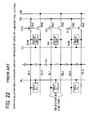
- FIG. 22 shows parasitic capacities existing between bit lines.
- memory cells containing memory cells Tc, Td, and Te or the like are disposed with high integrity, and thus, the bit lines BL1, /BL1, BL2, /BL2, BL3, and /BL3 or the like connected to these memory cells Tc, Td, and Te or the like run in parallel with each other adjacently. Therefore, parasitic capacity Cb exists between bit line pair and between the adjacent bit lines.
- FIG. 23A shows a time chart of writing in a bit line pair between a selected bit line BL1 and a complementary bit line /BL1 to which a memory cell Tc into which data is to be written is connected.
- FIG. 23B shows a time chart of readout from a memory cell Td for a refresh operation carried out in line with the adjacent bit line pair BL2 and /BL2.
- bit line short signal BRS When a bit line short signal BRS is deactivated, and a word line WL is activated, the stored charge is started to be redistributed into each of the bit lines BL1 and BL2 from the selected memory cells Tc and Td.
- data "1” is stored in the memory cell Tc, and thus, a potential of the bit line BL1 is started to rise.
- data "0” is stored in the memory cell Td, and thus, a potential of the bit line BL2 is started to fall.
- a switch signal CL1 is activated, and column switches TN1 and TN2 are made conductive.
- bit lines BL1 and /BL1 are connected.
- a potential of the bit line BL1 is inverted by means of a write amplifier (WA in FIG. 20), and is set to a low level side.
- the adjacent bit line BL2 is in the way of redistributing the stored charge from the memory cell Td. Since a potential difference between the bit line pair BL2 and /BL2 does not reach amplification sensitivity of the sense amplifier SAM, the sense amplifier SAM is in an inactive state. That is, the bit lines BL2 and /BL2 are in a floating state.
- the bit line BL1 set to the low level side and the bit line /BL2 in a floating state are adjacent, and the parasitic capacity Cb being a line parasitic capacity exists. Because of this, a voltage transition of the bit line BL1 is transmitted to be capacity coupled with the adjacent bit lines /BL2 as well.
- the voltage transition quantity of the adjacent bit line /BL2 is determined depending on the voltage transition quantity of the bit line BL1 caused by the amplification strength of the write amplifier WA, a potential difference between the adjacent bit line pair BL2 and /BL2, and a parasitic capacity Cb or the like.
- a potential difference between the adjacent bit line pair BL2 and /BL2 is reversed by means of an activation signal LE of the sense amplifier SAM, and is amplified, and readout of the stored charge may be reversed, which is problematic.
- This write noise does not always occur only between the adjacent bit lines.
- the easiness of noise propagation or the like changes variously due to manufacturing factors such as layout position relationship between a memory cell and a bit line, difference in dielectric constant of interline oxide film, or thickness of a metal wired layer.
- the present invention has been made in order to solve the foregoing problem with the prior art. It is an object of the present invention to provide a semiconductor integrated circuit device capable of, when a data writing operation for a memory cell is carried out by being embodied in a period during data readout from the memory cell for the adjacent bit lines, clamping a complementary bit line side of the adjacent bit line pair to a predetermined voltage, thereby reducing an effect of a write noise in a read operation for the adjacent bit lines, and making a constant operation.
- a semiconductor integrated circuit device comprises a plurality of memory cells, a plurality of word lines, and a plurality of bit line pairs, and further comprises a voltage fixing section for fixing to a predetermined voltage at least one bit line excluding a predetermined bit line or at least one bit line excluding the complimentary bit line of the predetermined bit line when data is written into the predetermined bit line or a complementary bit line of the predetermined bit line.
- a data writing method of a semiconductor integrated circuit device comprising: memory cells selected by a word line being activated; bit lines provided for each of the memory cells, and connected to the memory cells by selecting the word line, and complementary bit lines paired with the bit lines for amplifying data input from / output to the memory cell, the method comprising the voltage fixing step of, when data is written into a predetermined bit line or complementary bit line of the predetermined bit line, fixing to a predetermined voltage a plurality of complementary bit lines containing a complementary bit line of the predetermined bit line or a plurality of bit lines containing the predetermined bit line.
- a complementary bit line of the adjacent predetermined bit line to the predetermined bit line or a predetermined bit line adjacent to a complementary bit line of the predetermined bit line is set to a predetermined voltage by means of the voltage fixing section.
- a complementary bit line or a bit line that exist between the bit line or the complementary bit line to which a memory cell targeted for writing is connected and the adjacent bit lines or the adjacent complementary bit lines in which the stored charge is redistributed from a memory cell for the purpose of a refresh operation is fixed to a predetermined voltage.
- the capacity coupling caused by a voltage transition of a write bit line or write complementary bit line is shielded, thereby, a voltage transition can be prevented from being extended to the adjacent bit line or adjacent complementary bit line.
- One of the corresponding bit lines BLn and /BLn and the corresponding data buses DB and /DB are connected by these column switch signals CL0n and CL1n, and writing into a bit line is started.
- bit line short signals BRS0n and BRS1n from the bit line short signal circuit BSS1 are selected so as to shield a write noise that corresponding to the written, selected bit lines BLn and /BLn.
- bit lines BLn and /BLn For example, only two complementary bit lines /BLn and BLn adjacent to the written, selected bit lines BLn and /BLn can be selected so as to be fixed to a predetermined voltage VPR.
- a range of fixing to a predetermined voltage VPR can be further expanded and set.
- the complementary bit line /BLn or BLn that exists between bit line BLn or /BLn to which a memory cell targeted for writing is connected and the adjacent bit line BLn or /BLn in which redistribution of the stored charge from the memory cell is carried out for the purpose of refresh operation is fixed to predetermined voltage VPR. Because of this, the capacity coupling between bit lines containing the complementary bit line BLn or /BLn caused by the voltage transition of written bit line BLn or /BLn is shielded, and a noise caused by a voltage change can be prevented from being extended to the adjacent bit lines BLn or /BLn.
- the complementary bit lines /BLn or BLn fixed to a predetermined voltage VPR are set to the complementary bit lines /BLn or BLn containing but without being limited to both ends of a write bit line BLn or /BLn.
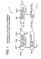
- a memory cell section 11 in a specific example of the first embodiment shown in FIG. 2 comprises: a bit line short signal circuit BSS1, bit line short circuits BS11 and BS12, and column switch signal circuits CS11 and CS12 instead of a bit line short signal circuit BSS, bit line short circuits BS and BSM, and column switch signal circuits CS and CSM of a memory cell section 1000 of the prior art shown in FIG. 20.
- An address signal A0 as well as an input signals in the prior art is further input to the bit line short signal circuit BSS1 and column switch signal circuits CS11 and CS12.
- An address signal A0 is a signal that determines memory cells Tc and Ta, Td and Tb connected to a bit line in which one of a set of bit line pairs BL1 and /BL1, BL2 and /BL2 are selected.
- the address signal A0 is set to its logical level, "low”
- the memory cells Tc, Td connected to the bit lines BL1, BL2 are selected, and the corresponding bit line short signal BRS0 and column switch signal CL01 are selectively output.
- a column address signals ADCn are selected at the same time.
- a column address signals ADCn as shown in the illustrative view 1 illustrating a principle shown in FIG.
- bit line short signal circuit BSS1 is not input to the bit line short signal circuit BSS1, and control for changing the adjacent complementary bit lines to be fixed to a predetermined voltage VPR corresponding to a write bit line is not carried out.
- bit lines free of writing are batch selected as a complementary bit lines, and are fixed to a precharge voltage VPR that is a determined voltage, whereby shielding of a write noise is carried out.
- Bit line short circuits BS11 and BS12 are circuits for precharging bit lines BL1 and BL2 or bit lines /BL1 and /BL2 to be fixed to precharge voltage VPR corresponding to bit line short signals BRS0 and BRS1.
- An address signal A0 as well an input signals in the prior art is further input to column switch signal circuits CS11 and CS12.
- a bit line pair BL1 and /BL1 or a bit line pair BL2 and /BL2 selected by means of the column address signals ADCn a bit line BL1, /BL1, BL2, or /BL2 to which memory cells Tc, Ta, Td, or Tb is connected corresponding to the address signal A0 is connected to a data bus DB or /DB, and thus, column switch signal CL01, CL11, CL02, or CL12 is activated, which makes the corresponding a column switch TN1, TN2, TN3, or TN4 conductive.
- FIG. 4 is a circuit example of bit line short circuits BS11 and BS12.
- FIG. 4 although a description is given by exemplifying a bit line pair BL1 and /BL1, a similar circuit configuration is obtained in another bit line pair as well.
- NMOS transistors SW11 and SW13 are connected in series, each of which is controlled by means of bit line short signals BRS0 and BRS1.
- bit lines BL1 and /BL1 are connected to a precharge voltage VPR by means of NMOS transistors SW12 and SW14 controlled by means of the bit line short signals BRS0 and BRS1.
- bit line short signals BRS0 and BRS1 When bit line short signals BRS0 and BRS1 are activated together, bit line pair BL1 and/BL1 is shorted. In addition, bit lines BL1 and /BL1 each are set to a precharge voltage VPR, and bit lines BL1 and /BL1 are in a precharge state. On the other hand, when either one of the bit line short signals BRS0 and BRS1 is activated, bit line pair BL1 and /BL1 is not shorted. While in an open circuit state, either one of the bit lines BL1 and /BL1 can be set to a precharge voltage VPR. Further, if the bit line short signals BRS0 and BRS1 are inactivated together, all the NMOS transistors SW11 to SW14 are in a nonconductive state, and normal readout / write state can be established.
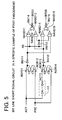
- FIG. 5 is a circuit example of a bit line short signal circuit BSS1.
- the input signals of the first and those of the second latch circuits configured by cross-coupling and connecting the NOR gates NOR11 and NOR12, NOR gates NOR13 and NOR14 respectively are an active signal ACT of a positive pulse as a set signal, and a precharge signal PRE of a positive pulse as a reset signal.
- the output signal of each of the latch circuits is inverted by means of each of the inverters INV11 and INV12, and is configured so that its logical level "high" is obtained during setting.
- a set input signal ACTD of a second input latch circuit is generated via a timing setting section t11 that configures a delay circuit by connecting inverter gates from an active signal ACT in predetermined even numbers.
- a NAND gate NAND 15 in which an output signal of a first latch circuit and an invert signal of an address signal A0 via an inverter INV 13 are input and a NAND gate NAND14 in which the output signal of a second input latch circuit and an address signal A0 are input generate a bit line short signal BRS0 via a NAND gate NAND 16 and an inverter INV 15.
- a NAND gate NAND 11 to which the output signal of the first input latch circuit and an address signal A0 are input, and a NAND gate NAND12 to which an output signal of a second latch circuit and an invert signal of the address signal A0 via the inverter INV 13 are input generate a bit line short signal BRS1 via the NAND gate NAND 13 and inverter INV 14.
- a first input latch circuit is set by means of an active signal ACT of a positive pulse to output its logical level signal "high”, and is reset by a precharge signal PRE of a positive pulse.
- a reset signal is obtained as a precharge signal PRE of a positive pulse in the same way as a first input latch circuit
- a set signal is obtained as a signal ACTD having a delay of a predetermined time via a timing setting section t1 from an active signal ACT of a positive pulse. Its logical level signal "high” is output after set by means of the delay signal ACTD.
- a bit line short signal BRS0 is obtained as its logical level "high”, and is activated when outputs of the NAND gate NAND14 and NAND15 each set to its logical level "high”.
- the bit line short signal BRS1 is obtained as its logical level "high”, and is activated when outputs of the NAND gates NAND 11 and NAND 12 each are set to its logical level "high”.
- a first input latch circuit is first set. If an address signal A0 is set to its logical level, "low”, an output signal of a NAND gate NAND 15 is status changed to its logical level “low”, and a bit line short signal BRS0 is status changed to its logical level, "low”, and is inactivated. If the address signal A0 is set to its logical level “high”, the output signal of the NAND gate NAND 11 is status changed to its logical level "low”, a bit line short signal BRS1 is status changed to its logical level "low”, and is inactivated.
- an active signal ACT is input to enter an access state, and a precharge operation for a bit line connected to a memory cell selected by the address signal A0 is released. Further, after an elapse of a delay time by a timing setting section t11, a second input latch circuit is set, and the output signal is inverted into its logical level "high”. Upon the receipt of this, if the address signal A0 is set to its logical level "low”, the output signal of NAND gate NAND12 is status changed to its logical level "low”. Then, the bit line short signal BRS1 is status changed to its logical level "low”, and is inactivated.
- FIG. 6 is a circuit example of column switch signal circuits CS11 and CS12.
- column switch signals CL0n and CL1n are generated as an output signal of each logical product composed of the NAND gate NAND19 and inverter INV1A, the NAND gate NAND18 and inverter INV19 respectively.
- An output signal of the inverter INV17 is input in common to the NAND gate NAND19 and the NAND gate NAND18.
- a signal obtained by inverting the address signal A0 by the inverter INV 18 and the address signal A0 are input each to the other input terminals.
- a column address signal ADCn is input to the inverter INV 17 via the NAND gate NAND 17, and an output signal of a third input latch circuit in which a control signal WC from the column control circuit CC is defined as a set signal, and a control signal WCD is obtained as a reset signal is input.
- a configuration of the third input latch circuit is composed of a cross couple connected NOR gates NOR 15, NOR 16, and an inverter INV16 as in a configuration of the first and second input latch circuits.
- the column switch signal circuits CS11 and CS12 are provided for each column address signals ADCn, and the third input latch circuit is set upon the receipt of a control signal WC of a positive pulse from the column control circuit CC relevant to the corresponding column address signals ADCn. Then, column switch signals CL0n and CL1n are generated so as to connect a bit line having connected thereto a memory cell selected by the address signal A0 to a data bus. The generated column switch signals CL0n and CL1n are reset upon the receipt of the control signal WCD of a positive pulse from the column control circuit CC.
- a bit line short signal BRS1 maintains its logical level "high" during predetermined period, and complementary bit lines /BL1 and /BL2 that are nonselective bit lines to which memory cells are not connected are fixed to a precharge voltage VPR, and a write noise is shielded.
- This time is defined as a shield period.
- a selective word line WL is activated, and the stored charge from the selected memory cells Tc and Td is redistributed to bit lines BL1 and BL2.
- a data bus short signal CPR is released by means of a control signal WR of a positive pulse
- a write amplifier WA is activated by means of an activation signal WAE
- write data (data "0" in FIG. 3) is amplified in the data buses DB and /DB.
- the amplified data is activated by means of the control signal WC of the positive pulse, and only the column switch signal CL01 is activated to make the column switch TN1 conductive.
- the bit line BL1 and data bus DB are connected with each other, and data is written into the bit line BL1.
- Data "1" is stored in the selected memory cell Tc.
- write data is set to "0”
- the data bus DB is shifted to its low level.
- the bit line BL1 is set to the low level side, and a write operation is carried out. This write state is carried out until a potential difference caused by writing of the bit line pair BL1 and/BL1 in which writing is carried out reaches the amplification sensitivity of the sense amplifier SA.
- bit lines BL2 and /BL2 are set to its floating state. Then, the complementary bit lines /BL1 and /BL2 that are nonselective bit lines to which memory cells are not connected are fixed to a precharge voltage VPR.
- bit lines BL1 and BL2 connected to the selected memory cells Tc and Td and the complementary bit lines /BL1 and /BL2 corresponding to nonselective memory cells Ta and Tb each can be set to a precharge voltage VPR independently.
- all the complementary bit lines /BL1 and /BL2 are selected altogether during write operation, and is simply and reliably fixed to the precharge voltage VPR so that a write noise can be shielded.
- a timing for being fixed to the precharge voltage VPR can be set, and thus, the complementary bit lines /BL1 and /BL2 are fixed to the precharge voltage VPR according to a period affected by the write noise so that a write noise can be properly shielded.
- bit lines BL1 and BL2 connected to memory cells Tc and Td that are selected memory cells and the complementary bit lines /BL1 and /BL2 corresponding to nonselective memory cells Ta and Tb are laid out alternatively, the voltage transition in the bit line BL1 for which write operation is carried out is simply and reliably shielded, and the voltage inversion of the adjacent bit lines /BL1, BL2, and /BL2 caused by a write noise can be prevented.
- column switches TN1 and TN3, column switches TN2 and TN4 configuring a switch section and a complementary switch section can be driven independently.
- bit lines BL1, BL2, /BL1, and /BL2 for example, there is no need to connect to the complementary data bus /DB the complementary bit line /BL1 paired with a predetermined bit line BL1 connected to the data bus DB.
- this complementary bit line /BL1 is fixed to its precharge voltage VPR so that a write noise for a predetermined bit line BL1 can be shielded.
- a data bus short signal CPR from the data bus short signal circuit DBSS and the bit line short signals BRS0n and BRS1n each are input to the data bus short circuit DBS2.
- data buses DB and /DB to be connected to the bit lines BLn and /BLn that correspond to each of the bit line short signals BRS0n and BRS1n are selected, and are fixed to a predetermined voltage VPR by being shorted.
- bit line short signals BRS0n and BRS1n are input to a write amplifier WA2 together with an activation signal WAE.
- the write amplifier WA2 does not carry out an amplifying operation for the data bus DB or /DB fixed corresponding to each of the bit line short signals BRS0n and BRS1n, and selects and amplifies only the data bus /DB or DB that is not fixed to the predetermined voltage VPR.
- the corresponding bit lines may be set so as not to be biased to a predetermined voltage during a predetermined time.
- a data bus short circuit DBS2 selects data bus DB or /DB, and fixes it to a predetermined voltage VPR. As a result, the corresponding bit lines are fixed to a predetermined voltage VPR by being shorted.
- a memory cell section 21 in a specific example of the second embodiment shown in FIG. 8 comprises a bit line short signal circuit BSS2, bit line short circuits BS21 and BS22, a data bus short circuit DBS2, and a write amplifier WA2 instead of the bit line short signal circuit BSS, the bit line short circuits BS and BSM, the data bus short circuit DBS, and the write amplifier WA of the memory cell section 1000 of the prior art shown in FIG. 20.
- An address signal A0 as well as input signals in the prior art is further input to the bit line short signal circuit BSS2.
- bit line short signal circuit BSS1 in a specific example of the first embodiment, if the address signal A0 is set to a logical level "low", the memory cells Tc and Td connected to the bit lines BL1 and BL2 are selected, and the corresponding bit line short signal BRS0 is selectively output.
- the column address signals ADCn as shown in the illustrative view 2 for a principle shown in FIG. 7 are not input to the bit line short signal circuit BSS2, and control for changing the adjacent bit lines to be fixed to a predetermined voltage VPR corresponding to a write bit line is not performed.
- bit line short circuits BS21 and BS22 are circuits for fixing bit lines BL1 and BL2 or bit lines /BL1 and /BL2 to a precharge voltage VPR corresponding to the bit line short signals BRS0 and BRS1 and precharging it.
- Bit line short signals BRS0 and BRS1 as well as input signals in the prior art are further input to a data bus short circuit DBS2.
- a bit line precharge voltage VPR is input as a precharge voltage of the data buses DB and /DB.
- bit lines BL1 and BL2 or bit lines /BL1 and /BL2 they are controlled by means of the bit line short signal BRS0 or BRS1 to be fixed to the same precharge voltage VPR.
- Bit line short signals BRS0 and BRS1 and the address signal A0 as well as input signals in the prior art are further input to the write amplifier WA2.
- bit lines BL1 and BL2 After the data buses DB and /DB have been connected to bit lines BL1 and BL2 or bit lines /BL1 and /BL2, data is written by means of the write amplifier WA2.
- the complementary bit line that is not connected to a memory cell is required to be fixed to the precharge voltage VPR for the purpose of shielding a write noise. Therefore, the write amplifier WA2 is controlled by means of the bit line short signals BRS0 and BRS1 and the address signal A0, and data is written only into a bit line to which a memory cell is connected.
- bit line short signals BRS0 and BRS1 if the address signal A0 is defined as an input signal, and a signal having the same phase as the bit line short signals BRS0 and BRS1 is generated, there can be provided operation or advantageous effect similar to the above description.
- bit line short signal circuit BSS2 has the same configuration as the bit line short signal circuit BSS1 in the first embodiment, and provides the same operation or advantageous effect. A duplicate description is omitted here.
- FIG. 10 is a circuit example of the data bus short circuit DBS2.
- This circuit has a circuit configuration similar to that of the bit line short circuits BS11 and BS12 (refer to FIG. 4) in a specific example of the first embodiment, and provides the similar operation or advantageous effect. If the bit line short signals BRS0 and BRS1 are activated altogether, data buses DB and /DB are shorted, and the data buses DB and /DB are fixed to a precharge voltage VPR and are set to a precharge state. When either one of the bit line short signals BRS0 and BRS1 is activated, the data buses DB and /DB are not shorted, and are kept to be released.
- either one of the data buses DB and /DB can be fixed to the precharge voltage VPR. Further, if the bit line short signals BRS0 and BRS1 are deactivated altogether, all the NMOS transistors DW21 to DW24 are made nonconductive, and are set to a normal readout / write state.
- FIG. 11 is a circuit example of a write amplifier WA2.
- Data bus DB is driven by means of a tri-state buffer that controls an output state by means of a PMOS transistor P21 and an NMOS transistor N22 that function as inverting buffers for input data Din and means of a PMOS transistor P22 and an NMOS transistor N21 connected in series to each of the buffer configured transistors.
- data bus /DB is driven by means of a tri-state buffer for controlling an output state by means of inverting buffers P23 and N24 having input thereto an inversion signal of data Din inverted by means of an inverter INV27 and P24 and N23 connected in series.
- control signals of each of the tri-state buffer driving data buses DB and /DB are obtained as an output signal via a inverter INV25 from a NAND gate NAND21 that configures a logical product between an activation signal WAE and each of an output signal of the inverter signal INV23 and an output signal of the inverter INV 24 and an output signal via an inverter INV26 from the NAND gate NAND22.
- These control signals are supplied after inverted by means of inverters INV28 and INV29, and an output state is controlled when PMOS transistor P22 and P24 are driven.
- the NOR gate NOR22 with the inverter 23 and the NOR gate NOR23 with the inverter 24 configure logical summation. Each logical summation is computed between an output signal from the NOR gate NOR 21 of the bit line short signals BRS0 and BRS1 and an inversion signal via the inversion INV 21 of the address signal A0, and further, a re-inversion signal caused by the inverter INV 22.
- the tri-state buffer at the data bus DB is set to an output enable state, the data Din is amplified and output.
- the tri-state buffer at the data bus /DB is set to an output high impedance state, and the data bus /DB is not amplified.
- address signal A0 is set to its logical level "high”
- logic is inverted and data bus /DB is amplified and data bus DB is not amplified.
- the data bus DB is amplified, and write operation is carried out for either of the bit lines BL1 and BL2.
- the data bus short circuit DBS2 fixes the complementary bit lines /BL1 and /BL2 to the precharge voltage VPR.
- the data bus /DB is amplified, and write operation is carried out for either of the bit lines /BL1 and /BL2.
- the data bus short circuit DBS2 fixes the complementary bit line BL1 and BL2 to the precharge voltage VPR.
- the complementary bit lines /BL1 and /BL2 or the bit lines BL1 and BL2 are controlled by means of bit line short signals BRS1 and BRS0, and are fixed to the precharge voltage VPR by means of bit line short circuits BS21 and BS22. Therefore, in the write amplifier WA2, if driving of the data bus /DB or DB connected to the complementary bit lines /BL1 and /BL2 or the bit lines BL1 and BL2 is stopped, there is no need to make a fixing operation for the precharge voltage VPR by means of the data bus short circuit DBS2.
- the data bus DB or /DB is precharged to a high level, and one of them is reduced to a low level during amplification.
- the data bus DB or /DB is precharged to the voltage level of the precharge voltage VPR.
- the data bus DB or /DB is precharged to the voltage level of the precharge voltage VPR.
- the data bus DB is first amplified (in the case of FIG. 9, the data bus is amplified to a low level).
- the sense amplifier SA and SAM are activated by means of an activation signal LE.
- the other operation is similar to the first embodiment (refer to FIG. 3) or prior art (refer to FIG. 21). A duplicate description is omitted here.
- the complementary data line /DB can be driven by means of a precharge voltage VPR that is a predetermined voltage at a timing set by a timing setting section t11 in the bit line short signal circuit BSS 2.
- VPR a precharge voltage
- the bit line /BL1 that is a complementary bit line can be fixed to a precharge voltage VPR for the purpose of shielding while there is employed a simple control configuration in the prior art in which the column switches TN1 and TN2 are controlled in common.
- bit lines BL1 and BL2 connected to the selected memory cells Tc and Td and the complementary bit lines /BL1 and /BL2 corresponding to nonselective memory cells Ta and Tb can be fixed independently to the precharge voltage VPR that is a predetermined voltage.
- the complementary bit lines /BL1 and /BL2 to be fixed can be selected in batch without a need to select these bit lines corresponding to the write bit line BL1.
- all the complementary bit lines /BL1 and /BL2 are selected altogether, and are simply and reliably fixed to the precharge voltage VPR, whereby a write noise can be shielded.
- a timing for fixing to the precharge voltage VPR can be set.
- the complementary bit lines /BL1 and /BL2 can be fixed to the precharge voltage VPR according to a period affected by a write noise, whereby a write noise can be properly shielded.
- bit lines BL1 and BL2 connected to selected memory cells Tc and Td and the complementary bit lines /BL1 and /BL2 corresponding to nonselective memory cells Ta and Tb are laid out alternately, a voltage transition in a bit line BL1 for which a write operation is carried out is simply and reliably shielded, and the voltage reversal of the adjacent bit lines /BL1, BL2, and /BL2 caused by a write noise can be prevented.
- bit line short signals BRS0 and BRS1 are selected and activated, and is input to a bit line short circuit BS21, whereby the corresponding complementary bit line /BL1 is fixed to a predetermined voltage VPR after being shorted during a predetermined time.
- the corresponding complementary bit line /BL1 may be set so as not to be biased to a predetermined voltage during a predetermined time.
- the data bus short circuit DBS2 selects a data bus /DB, and is fixed to a predetermined voltage VPR after being shorted. As a result, the corresponding complementary bit line /BL1 is fixed to a predetermined voltage VPR after being shorted.
- an address signal A0 for determining which of a bit line pair other than control signals WR and WCD is selected is input to a data bus short signal circuit DBSS3.
- a data bus short signal DBSS is activated by selecting data bus short signals CPR1 and CPR2, and the activated signal is input to a data bus short circuit DBS3, and the corresponding data bus DB or /DB is fixed to a predetermined voltage VPR during a predetermined time after being shorted.
- the input signals are controlled by means of the control signals WC and WCD
- all the other complementary bit line /BLn or BLn is activated so as to be connected to the data bus /DB or DB.
- the data bus short signals CPR1 and CPR2 and the address signal A0 are input to the write amplifier WA3.
- the write amplifier WA3 amplifies data relevant to the data bus DB or /DB connected to the bit line BLn or /BLn for which write operation is carried out. This amplifier does not carries out an amplification operation for the data bus /DB or DB connected to the bit line /BLn or BLn for which write operation is not carried out.
- a bit line /BLn or BLn that is a complementary bit line is fixed to a precharge voltage VPR from the data bus /DB or DB that is a complementary data line fixed to a precharge voltage VPR that is a predetermined voltage via a column switch that is a conductive complementary switch section.
- complementary bit lines containing predetermined complementary bit lines /BLn or BLn can be fixed to a precharge voltage VPR without providing individual clamp portions that can be driven independently by properly dividing the bit lines and complementary bit lines.
- a memory cell section 31 in a specific example of the third embodiment shown in FIG. 13 comprises: column switch signal circuits CS31 and CS32; a data bus short signal circuit DBSS3, a data bus short circuit DBS3; and a write amplifier WA3 instead of the column switch signal circuit CS, CSM, data bus short signal circuit DBSS, data bus short circuit DBS, and write amplifier WA of a memory cell section 1000 according to the prior art shown in FIG. 20.
- An address signal A0 is input to the column switch signal circuits CS31 and CS32 as in the column switch signal circuits CS11 and CS12 according to the first embodiment.
- the column address signals ADCn and an address signal A0 in order to connect to the data bus DB or /DB a bit line BL1, /BL1, BL2, or /BL2 for which write operation should be carried out, of bit line pair BL1 and /BL1 and bit line pair BL2 and /BL2, and all the complementary bit lines each having a complementary relation with a selected bit line, to be fixed to the precharge voltage VPR, the column switch signal circuits CS31 and CS32 activates column switch signals CL01, CL11, CL02, or CL12 for making the corresponding column switches TN1 to TN4 conductive.
- An address signal A0 as well as input signals in the prior art are further input to the data bus short signal circuit DBSS3.
- the data bus short signal circuit DBSS3 releases data bus DB or /DB connected to the bit lines BL1, BL2 or /BL1, /BL2, respectively, from the precharge voltage VPR.
- the bit lines BL1, BL2", /BL1, and /BL2 correspond to the address signal A0.
- the data bus short signal circuit DBSS3 outputs the data bus short signals CPR1 and CPR2 for continuously fixing to the precharge voltage VPR to the data bus short circuit DBS3.
- the complementary bit lines /BL1, /BL2, BL1, and BL2 have complementary relation with bit lines /BL1, /BL2, BL1, and BL2, respectively.
- the precharge voltage VPR of the data buses DB and /DB as well as input signals in the prior art is further input to the data bus short circuit DBS3. Then, control for fixing the data bus DB or /DB to the precharge voltage VPR according to the data bus short signals CPR1 and CPR2 is carried out.
- Data bus short signals CPR1 and CPR2 and an address signal A0 as well as input signals in the prior art are further input to a write amplifier WA3.
- Data bus DB or /DB is connected to bit lines BL1, BL2, /BL1, or /BL2 and the like for which write operation is carried out, data is amplified by means of a write amplifier WA3, and write operation is carried out.
- the complementary bit lines /BL1 and /BL2 or bit lines BL1 and BL2 that are not connected to a memory cell are required to be fixed to the precharge voltage VPR for the purpose of shielding a write noise.
- the data bus /DB or DB for which write operation is not carried out is connected by selecting the complementary bit lines /BL1 and /BL2 or bit lines BL1 and BL2 for which a memory cell is not connected altogether.
- a write amplifier WA3 is controlled by means of the data bus short signals CPR1 and CPR2 and the address signal A0, and the precharge voltage VPR is supplied.
- the address signal A0 is defined as an input signal instead of the data bus short signals CPR1 and CPR2, operation and advantageous effect similar to the above description can be achieved.
- FIG. 15 is a circuit example of the column switch signal circuits CS31 and CS32.
- the column switch signal circuits CS31 and CS32 generates column switch signals CL0n and CL1n as output signals of logical products each composed of the NAND gate NAND32 and inverter INV36 and the NAND gate NAND31 and inverter INV35.
- an output signal of a fourth input latch circuit composed of the cross coupled NOR gates NOR 31 and NOR 32 and the inverter INV31, a control signal WC being defined as a set signal, and a control signal WCD being defined as a reset signal, is connected in common to a NAND gate NAND32 and a NAND gate NAND31.
- column address signals ADCn and an address signal A0 are logically summed and input to the NAND gate NAND32 via the NOR gate NOR34 and the inverter INV 34.
- a configuration of a fourth input latch circuit is similar to that of an input latch circuit according to first to third embodiments.
- the column switch signal circuits CS31 and CS32 are provided every column address signals ADCn. Upon the receipt of a control signal WC of a positive pulse from the column control circuit CC, the fourth input latch circuit is set. Then, the column switch signal circuits CS31 and CS32 activates the column switch signals CL0n and CL1n that correspond to the selected column address signals ADCn, connect bit line pair BL1 and /BL1 or bit line pair BL2 and /BL2 for which write operation is carried out with data bus DB and /DB.
- the column switch signals CL1n are activated, and the bit lines /BL1 and /BL2 and the data bus /DB are connected with each other.
- the address signal A0 is set to a logical level "high”
- column switch signals CL0n are activated and bit lines BL1, BL2 are connected to data bus DB.
- bit lines BL1 and BL2 are connected to a memory cell, and when the address signal A0 is set to a logical level "high”, bit lines /BL1, /BL2 are connected to a memory cell, and thus, the complementary bit line not to be connected to a memory cell are connected with the data bus.
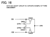
- FIG. 16 is a circuit example of a data bus short circuit DBS3. Except that the data bus short signals CPR1 and CPR2 are connected instead of the bit line short signals BRS0 and BRS1 in the data bus short circuit DBS2 (refer to FIG. 10) according to the second embodiment, the construction is similar to that of the data bus short circuit DBS2 according to second embodiment, the similar operation and advantageous effect are provided. A description of such similar operation and advantageous effect is omitted here.
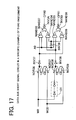
- FIG. 17 is a circuit example of a data bus short signal circuit DBSS3.
- This circuit has a circuit configuration similar to the bit line short signal circuit BSS1 (refer to FIG. 5) according to the first embodiment.
- a control signal WR from the column control circuit CC is input instead of the active signal ACT in the bit line short signal circuit BSS1.
- a control signal WCD from the column control circuit CC is input instead of the precharge signal PRE.
- the data bus short signals CPR1 and CPR2 are output instead of the bit line short signals BRS0 and BRS1.
- a fifth input latch circuit composed of NOR gates NOR36 and NOR37 and inverter INV37 is first set. If the address signal A0 is set to its logical level "low”, an output signal of the NAND gate NAND36 is status changed to its logical level “low”. The data bus short signal CPR1 is status changed to its logical level “low”, and is inactivated. When the address signal A0 is set to its logical level "high”, an output signal of the NAND gate NAND33 is status changed to its logical level "low”. In addition, the data bus short signal CPR2 as well is status changed to its logical level "low”, and is inactivated.
- a control signal WR is input to enter an access state, and a precharge operation for a selective bit line selected by the address signal A0 is released. Further, after an elapse of a delay time caused by a timing setting section t31, a sixth input latch circuit composed of the NOR gates NOR38 and NOR39 and inverter INV38 is set, and an output signal is inverted into its logical level "high” . Upon the receipt of this, if the address signal A0 is set to its logical level "low”, an output signal of the NAND gate NAND34 is status changed to its logical level "low”. Then, the data bus short signal CPR2 is status changed to its logical level "low”, and is inactivated.
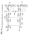
- FIG. 18 is a circuit example of a write amplifier WA3.
- a basic circuit configuration is similar to that of a write amplifier WA2 according to the second embodiment (refer to FIG. 11).
- the write amplifier WA3 comprises inverters INV3E and INV3F instead of a NOR gate NOR21 in the write amplifier WA2.
- the data bus short signal CPR1 is input to the inverter INV3E, and the data bus short signal CPR2 is input to the inverter INV3F.
- the respective output signals are input to the NOR gates NOR3A and NOR3B each as in the NOR gate NOR21 in the write amplifier WA2.
- Theother configuration is similar to that of the write amplifier WA2 according to the second embodiment. A duplicate description is omitted here.
- the write amplifier WA3 is controlled by means of the address signal A0. That is, in the case where the address signal A0 is set to its logical level "low", a tri-state buffer at the data bus DB is set to an output enable state by means of an activation signal WAE, and the data Din is amplified and output. In contrast, the tri-state buffer on the data bus /DB is set to an output high impedance state, and data bus /DB is not amplified. In the case where the address signal A0 is set to its logical level "high”, the logic is inverted. Thus, the data bus /DB is amplified, and the data bus DB is not amplified.
- the data bus DB is amplified, and write operation is carried out for either of the bit lines BL1 and BL2.
- the data bus short circuit DBS3 fixes the complementary bit lines /BL1 and /BL2 to the precharge voltage VPR.
- the address signal A0 is set to its logical level "high”
- the bit lines /BL1 and /BL2 are selected
- the data bus /DB is amplified, and write operation is carried out for either of the bit lines /BL1 and /BL2.
- data bus short circuit DBS3 fixes the complementary bit lines BL1, and BL2 to the precharge voltage VPR.
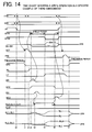
- the data bus short signal CPR2 maintains its logical level "high" during a predetermined period. Then, the data bus /DB is fixed to the precharge voltage VPR, whereby the complementary bit lines /BL1 and /BL2 that are nonselective bit lines to which a memory cell are not connected are fixed to the precharge voltage VPR, and a write noise is shielded. This time is defined as a shield period.
- the selected word line WL is activated, and the stored charge is redistributed from the memory cells Tc and Td selected for the bit lines BL1 and BL2.
- the data bus short signal CPR1 is released by means of the control signal WR of the positive pulse.
- the write amplifier WA3 is activated by means of the activation signal WAE, and write data is amplified for only the data bus DB (in the case of FIG. 14, data "0" is amplified) .
- the amplified data is activated by means of the control signal WC of the positive pulse, and the column switch signals CL01, CL11, and CL12 are activated to make the column switches TN1, TN2, and TN4 conductive.
- bit line BL1 and data bus DB are connected with each other, data is written into the bit line BL1, and the complementary bit lines /BL1 and /BL2 are fixed to the precharge voltage VPR.
- data "1" is stored in the selected memory cell Tc, and the bit line BL1 is shifted to the high level side, the write data is obtained as data "0".
- the data bus DB is shifted to the low level.
- the bit line BL1 is set to the low level side, and write operation is carried out. This write status is maintained until a potential difference caused by writing of bit line pair BL1 and /BL1 for which write operation is carried out has reached the amplification sensitivity of the sense amplifier SA.
- the stored charge from the memory cell Td is redistributed in order to carry out refresh operation in another bit line BL2.
- This redistribution continues until a potential difference between the bit line pair BL2 and /BL2 has reached the amplification sensitivity caused by the sense amplifier SAM.
- the bit lines BL2 and /BL2 are in a floating state.
- the complimentary bit lines /BL1 and /BL2 to which a memory cell is not connected are set to the precharge voltage VPR, whereby the voltage transition caused by the write operation is prevented from propagating the adjacent bit line BL2 or complementary bit lines /BL1 and /BL2 via the parasitic capacity Cb which results in incorrect data inversion.
- the sense amplifier SA and SAM are activated by means of an activation signal LE, and amplification is carried out.
- the subsequent operation is similar to that according to the prior art (refer to FIG. 21).
- VPR precharge voltage
- bit lines BL1 and BL2 connected to memory cells Tc and Td that are the selected memory cells and the complimentary bit lines /BL1 and /BL2 that correspond to the memory cells Ta and Tb that are nonselective memory cells can be fixed to the precharge voltage VPR that is a predetermined voltage, independently, and moreover, the complimentary bit lines /BL1 and /BL2 to be fixed can be selected altogether without a need to select them corresponding to the write bit line BL1.
- all the complementary bit lines /BL1 and /BL2 are selected altogether, and are simply and reliably fixed to the precharge voltage VPR, whereby a write noise can be shielded.
- a timing for fixing to the precharge voltage VPR can be set.
- the complimentary bit lines /BL1 and /BL2 are fixed to the precharge voltage VPR according to a period affected by a write noise, whereby a write noise can be properly shielded.
- bit lines BL1 and BL2 connected to the selected memory cells Tc and Td or the like and the complementary bit lines /BL1 and /BL2 corresponding to the nonselective memory cells Ta and Tb are laid out alternately, a voltage transition in bit line BL1 for which write operation is carried out is simply and reliably shielded, whereby the voltage reversal of the adjacent bit lines /BL1, BL2, and /BL2 caused by a write noise can be prevented.
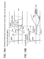
- FIG. 19 shows a write operation waveform in the case of a specific example according to the first embodiment. The figure shows that an effect of a write noise is eliminated by using a comparison with the write operation waveform in the case of the prior art in FIG. 23.
- FIG. 19A shows a time chart of a write operation in a pair of selective bit line BL1 and complementary bit line /BL1 having connected thereto a memory cell Tc into which data is to be written.
- FIG. 19B shows a time chart for reading out the stored charge from the memory cell Td for the purpose of refresh operation carried out at the same time with the adjacent bit line pair BL2 and /BL2.
- bit line short signal BRS0 When a bit line short signal BRS0 is inactivated, and a word line WL is activated, the stored charge is started to be redistributed from the selected memory cells Tc and Td to each of the bit lines BL1 and BL2. A potential of the bit line BL1 is started to rise according to the stored charge of each of the memory cells Tc and Td, and a potential of the bit line BL2 is started to fall. Next, a switch signal CL01 is activated, and only a column switch TN1 is made conductive. Then, a connection between the data bus line DB amplified at a proper timing with activation of the word line WL and the bit line BL1 is made for the purpose of write operation for the memory cell Tc.
- bit line BL1 Because of writing of data "0", a potential of the bit line BL1 is reversed by means of a write amplifier WA, and is set to its low level side. At this stage, the adjacent bit line BL2 is in way of redistribution of the stored charge from the memory cell Td, and a potential difference between the bit line pair BL2 and /BL2 does not reach the amplification sensitivity of the sense amplifier SAM. Thus, the sense amplifier SAM is in an inactive state. That is, the bit line BL2 is in a floating state.
- bit line short signal BRS1 maintains its logical level "high" in this duration, and the complementary bit lines /BL1 and /BL2 that are nonselective bit lines are fixed to the precharge voltage VPR, whereby a write noise is shielded.
- the complementary bit line /BL2 is adjacent to the bit line BL1 set to the low level side, and a parasitic capacity Cb exists as a parasitic capacity.
- the adjacent complimentary bit lines /BL1 and /BL2 are fixed to the precharge voltage VPR, and thus, the voltage transition caused by write operation for the bit line BL1 is shielded by means of the adjacent complementary bit lines /BL1 and /BL2.
- the complimentary bit lines /BL1 and /BL2 each are fixed to the precharge voltage VPR without depending on the amount of voltage transition of the bit line BL1 caused by the amplification strength of the write amplifier WA, the potential difference between the adjacent bit line pair BL2 and /BL2, or the parasitic capacity Cb and the like. In this manner, a write noise during data writing into the bit line BL1 is shielded, a refresh operation in the adjacent bit line pair BL2 and /BL2 is normally carried out, and the memory data is not inverted.
- the complimentary bit lines /BL1 and /BL2 connected to the complimentary data bus /DB are fixed to the precharge voltage VPR by means of the bit line short circuits BS21 and BS22. Because of this, for example, at the initial write stage for the bit line BL1, it is possible to set the complimentary data bus /DB so as not to be driven.
- the column address signals ADCn and an address signal A0 are input to bit line short signal circuits BSS1 and BSS2, and the bit line short signal BRS0n and BRS1n are output.
- the column address signals ADCn and an address signal A0 are input to the column switch signal circuits CS3n, and the column switch signals CL0n and CL1n are output.
- This illustrative view illustrates a case in which the adjacent bit lines are fixed to the precharge voltage VPR according to the bit line BLn or /BLn targeted for writing.
- a combination for fixing to the precharge voltage VPR can be changed as required. For example, it is possible to specify a region for fixing to the precharge voltage VPR by dividing the memory cells into sub-blocks.
- the precharge voltage VPR is utilized so as to shield a write noise
- another voltage source can be utilized without being limited thereto as long as a stationary potential is provided.
- bit lines /BL1 and /BL2 are defined as complementary bit lines relevant to bit lines BL1 and BL2. This is because the memory cells Tc and Td connected to the bit lines BL1 and BL2 are selected by the word line WL. Therefore, of course, this applies to a case in which the memory cells Ta and Tb are selected, thereby reversing a relationship between a bit line and its complimentary bit line.
- a semiconductor integrated circuit device in which, when a data write operation for a memory cell is carried out by fitting it in a period while in data reading from the memory cell for the adjacent bit lines, the complimentary bit line side in the adjacent bit line pair is clamped to a predetermined voltage, whereby an effect of a write noise in a readout operation for the adjacent bit lines is reduced, making it possible to ensure stable operation.
Landscapes
- Dram (AREA)
- Read Only Memory (AREA)
- Semiconductor Memories (AREA)
Abstract
Description
Claims (20)
- A semiconductor integrated circuit device comprising a plurality of memory cells, a plurality of word lines, and a plurality of bit line pairs, the circuit device comprising a voltage fixing section for, when data is written into a predetermined bit line or a complimentary bit line of the predetermined bit line, fixing to a predetermined voltage at least one bit line excluding the predetermined bit line or at least one bit line excluding the complimentary bit line of the predetermined bit line.
- A semiconductor integrated circuit device as claimed in claim 1, wherein the voltage fixing section fixes to the predetermined voltage a plurality of complimentary bit lines containing the complimentary bit line of the predetermined bit line or a plurality of bit lines containing the predetermined bit line.
- A semiconductor integrated circuit device as claimed in claim 2, further comprising a plurality of clamp sections for independently fixing to the predetermined voltage the plurality of bit lines each and the plurality of complementary bit lines each during a period when the word line is not activated, wherein the voltage fixing section comprises: a selecting section for properly selecting the clamp section; and a timing setting section for setting a timing for fixing to the predetermined voltage the complimentary bit line of the predetermined bit line or the predetermined bit line after the word line is activated.
- A semiconductor integrated circuit device as claimed in claim 1, further comprising: a first clamp section for fixing to a predetermined voltage a bit line during a period when the word line is not activated; and a second clamp section for fixing to a predetermined voltage a complimentary bit line during a period when the word line is not activated, wherein the voltage fixing section comprises: a selecting section for selecting the second clamp section or the first clamp section; and a timing setting section for setting a timing for fixing to the predetermined voltage the complimentary bit line of the predetermined bit line or the predetermined bit line after the word line is activated.
- A semiconductor integrated circuit device as claimed in claim 3, further comprising:a switch section for connecting a bit line with a data line for data transfer;a complimentary switch section for connecting a complimentary bit line with a complimentary data line paired with the data line; anda switch selecting section for making conductive the switch section that corresponds to the predetermined bit line or the complimentary switch section that corresponds to the complimentary bit line of the predetermined bit line, and making nonconductive the complimentary switch section or the switch section at the timing.
- A semiconductor integrated circuit device as claimed in claim 1, further comprising:a switch section for connecting a bit line with a data line for data transfer;a complimentary switch section controlled in common with the switch section, the complimentary switch section connecting a complimentary bit line with a complimentary data line paired with the data line; anda timing setting section for, after the word line has been activated, setting a timing for fixing to the predetermined voltage the complimentary bit line of the predetermined bit line or the predetermined bit line, wherein, when data is written, only the data line or the complimentary data line is amplified at a timing set by the timing setting section prior to amplifying data to be written when the data line and the complimentary data line are paired.
- A semiconductor integrated circuit device as claimed in claim 6, further comprising a plurality of clamp sections for independently fixing to the predetermined voltage the plurality of bit lines each and the plurality of complimentary bit lines each during a period when the word line is not activated, wherein the voltage fixing section has a selecting section for selecting the plurality of clamp sections as required, and the complimentary data line or the data line are not driven at a timing set by the timing setting section before data to be written is amplified when the data line and the complimentary data line are paired.
- A semiconductor integrated circuit device as claimed in claim 6, wherein the complimentary data line or the data line are driven with the predetermined voltage at a timing set by the timing setting section before data to be written is amplified when the data line and the complimentary data line are paired.
- A semiconductor integrated circuit device as claimed in claim 1, further comprising: a switch section for connecting a bit line with a data line for data transfer; and a complimentary switch section for connecting a complimentary bit line with a complimentary data line paired with the data line, wherein the voltage fixing section comprises: a switch selecting section for, when data is written, making conductive the switch section or the complimentary switch section for the predetermined bit line or the complimentary bit line of the predetermined bit line and the complimentary switch section or the switch section; a timing setting section for, after the word line has been activated as well, setting a timing for fixing to the predetermined voltage the complimentary bit line or the bit line; and a clamp section for fixing to the predetermined voltage the complimentary data line or the data line at a timing set by the timing setting section before data to be written is amplified when the data line and the complimentary data line are paired.
- A semiconductor integrated circuit device as claimed in claim 2, further comprising: a switch section for connecting a bit line with a data line for data transfer; and a complimentary switch section for connecting a complimentary bit line with a complimentary data line paired with the data line, wherein the voltage fixing section comprises:a switch selecting section making conductive the switch section or the complimentary switch section for the predetermined bit line or the complimentary bit line of the predetermined bit line, and the complimentary switch section or the switch section for the plurality of complimentary bit line or the plurality of bit lines, and making nonconductive the switch section or the complimentary switch section for the bit line or the complimentary bit line having connected thereto a memory cell for which data writing is not carried out;a timing setting section for, after the word line has been activated as well, setting a timing for fixing to the predetermined voltage the plurality of complimentary bit lines or the plurality of bit lines; anda clamp section for fixing to the predetermined voltage the complimentary data line or the data line at a timing set by the timing setting section before data to be written is amplified when the data line and the complimentary data line are paired.
- A semiconductor integrated circuit device as claimed in claim 1, wherein, after a potential difference between a voltage value written into the predetermined bit line or the complimentary bit line of the predetermined bit line and a voltage value of the complimentary bit line paired with the predetermined bit line or the predetermined bit line paired with the complimentary bit line of the predetermined bit line has reached a amplification threshold value, fixing the complimentary bit line or the bit line to the predetermined voltage is released.
- A semiconductor integrated circuit device as claimed in claim 11, further comprising a sense amplifier for amplifying a potential difference between the bit line and the complimentary bit line, wherein the amplification threshold value is equal to or greater than a voltage value of amplification sensitivity of the sense amplifier.
- A semiconductor integrated circuit device as claimed in claim 1, wherein selection of the memory cell and reading out or writing the data from/to the memory cell are carried out by one command entry.
- A semiconductor integrated circuit device as claimed in claim 13, wherein the memory cell comprises a capacity element, and stores the data according to whether charge storage in the capacity element is present or absent.
- A data writing method in a semiconductor integrated circuit device comprising: memory cells selected by a word line being activated; bit lines provided corresponding to each of the memory cells, the bit lines being connected to the memory cells according to selection of the word line; and a complimentary bit lines paired with the bit lines, the complimentary bit lines being adopted to amplify data input to / output from the memory cells, wherein the writing method comprises a voltage fixing step of, when data is written into a predetermined bit line or a complimentary bit line of a predetermined bit line, fixing to a predetermined voltage a plurality of complimentary bit lines containing the complimentary bit line of the predetermined bit line or a plurality of bit lines containing the predetermined bit line.
- A data writing method in the semiconductor integrated circuit device as claimed in claim 15, the method comprising:a selecting step of, from among a plurality of clamp sections for independently fixing to the predetermined voltage the plurality of bit lines each and the plurality of complimentary bit lines each, selecting the clamp section for fixing to the predetermined voltage the plurality of complimentary bit lines or the plurality of bit lines; anda timing setting step of setting a period when the selected clamp section is activated to a predetermined period from after activation of the word line.
- A data writing method in the semiconductor integrated circuit device as claimed in claim 16, further comprising a switch selecting step of, during the predetermined period, making conductive a switch section that corresponds to the predetermined bit line or a complimentary switch section that corresponds to a complimentary bit line of the predetermined bit line, and making nonconductive the complimentary switch section or the switch section.
- A data writing method in the semiconductor integrated circuit device as claimed in claim 15, wherein, in the predetermined period before data to be written is amplified when a data line connected to the bit line is paired with a complimentary data line connected to the complimentary bit line, the complimentary data line or the data line is not driven or fixed to the predetermined voltage, only the data line or the complimentary data line is amplified.
- A data writing method in the semiconductor integrated circuit device as claimed in claim 15, further comprising:a switch selecting step of make conductive a switch section between the predetermined bit line and a data line for data transfer or a complimentary switch section between a complimentary bit line of the predetermined bit line and a complimentary data line for data transfer and a complimentary switch section between each of the plurality of complimentary bit lines and the complimentary data line or a switch section between each of the plurality of bit lines and the data line, and keep nonconductive the switch section between the bit line or the complimentary bit line for which data writing is not carried out and the data line or the complimentary data line; anda timing setting step of setting to the predetermined period prior to data to be written is amplified when the data line and the complimentary data line are paired from after activation of the word line, a period for activating the complimentary switch section or the switch section, for connecting the plurality of complimentary bit lines or the plurality of bit lines selected in accordance with the switch selecting step with the complimentary data line or the data line, wherein, in the predetermined period, the complimentary data line or the data line is fixed to the predetermined voltage.
- A data writing method in the semiconductor integrated circuit device as claimed in claim 15, wherein, after a potential difference between a voltage value written into the predetermined bit line or a complimentary bit line of the predetermined bit line and a voltage value of the complimentary bit line paired with the predetermined bit line or the predetermined bit line paired with a complimentary bit line of the predetermined bit line has reached an amplification threshold value, fixing of the complimentary bit line to the predetermined voltage is released.
Applications Claiming Priority (2)
| Application Number | Priority Date | Filing Date | Title |
|---|---|---|---|
| JP2001180923 | 2001-06-15 | ||
| JP2001180923A JP2002373491A (en) | 2001-06-15 | 2001-06-15 | Semiconductor storage device |
Publications (2)
| Publication Number | Publication Date |
|---|---|
| EP1267353A2 true EP1267353A2 (en) | 2002-12-18 |
| EP1267353A3 EP1267353A3 (en) | 2004-03-24 |
Family
ID=19021266
Family Applications (1)
| Application Number | Title | Priority Date | Filing Date |
|---|---|---|---|
| EP01129839A Withdrawn EP1267353A3 (en) | 2001-06-15 | 2001-12-14 | Semiconductor integrated circuit device and data writing method therefor |
Country Status (4)
| Country | Link |
|---|---|
| US (1) | US6741518B2 (en) |
| EP (1) | EP1267353A3 (en) |
| JP (1) | JP2002373491A (en) |
| KR (1) | KR100759770B1 (en) |
Families Citing this family (12)
| Publication number | Priority date | Publication date | Assignee | Title |
|---|---|---|---|---|
| US9208902B2 (en) * | 2008-10-31 | 2015-12-08 | Texas Instruments Incorporated | Bitline leakage detection in memories |
| US9741413B2 (en) | 2014-09-25 | 2017-08-22 | Kilopass Technology, Inc. | Methods of reading six-transistor cross-coupled thyristor-based SRAM memory cells |
| US9613968B2 (en) | 2014-09-25 | 2017-04-04 | Kilopass Technology, Inc. | Cross-coupled thyristor SRAM semiconductor structures and methods of fabrication |
| US9530482B2 (en) | 2014-09-25 | 2016-12-27 | Kilopass Technology, Inc. | Methods of retaining and refreshing data in a thyristor random access memory |
| US9564441B2 (en) | 2014-09-25 | 2017-02-07 | Kilopass Technology, Inc. | Two-transistor SRAM semiconductor structure and methods of fabrication |
| US9564199B2 (en) | 2014-09-25 | 2017-02-07 | Kilopass Technology, Inc. | Methods of reading and writing data in a thyristor random access memory |
| US20160093624A1 (en) | 2014-09-25 | 2016-03-31 | Kilopass Technology, Inc. | Thyristor Volatile Random Access Memory and Methods of Manufacture |
| US9460771B2 (en) | 2014-09-25 | 2016-10-04 | Kilopass Technology, Inc. | Two-transistor thyristor SRAM circuit and methods of operation |
| US9449669B2 (en) * | 2014-09-25 | 2016-09-20 | Kilopass Technology, Inc. | Cross-coupled thyristor SRAM circuits and methods of operation |
| TWI745392B (en) | 2017-06-29 | 2021-11-11 | 瑞禾生物科技股份有限公司 | Biosensor device and method for manufacturing thereof and method for detecting biological molecule |
| US10459871B2 (en) * | 2017-09-13 | 2019-10-29 | Micron Technology, Inc. | Switching reduction bus using data bit inversion with shield lines |
| CN115729573A (en) * | 2021-09-01 | 2023-03-03 | 富联精密电子(天津)有限公司 | Firmware upgrading method, device, chip and computer storage medium |
Family Cites Families (14)
| Publication number | Priority date | Publication date | Assignee | Title |
|---|---|---|---|---|
| JPS6457493A (en) * | 1987-08-28 | 1989-03-03 | Mitsubishi Electric Corp | Semiconductor memory device |
| JPH01277390A (en) * | 1988-04-28 | 1989-11-07 | Mitsubishi Electric Corp | Semiconductor storage device |
| JP2755615B2 (en) * | 1988-09-28 | 1998-05-20 | 株式会社東芝 | Semiconductor storage device |
| US5010523A (en) | 1989-03-06 | 1991-04-23 | Matsushita Electric Industrial Co., Ltd. | Sensing circuit for a dynamic random access memory |
| US5010524A (en) * | 1989-04-20 | 1991-04-23 | International Business Machines Corporation | Crosstalk-shielded-bit-line dram |
| JPH0541085A (en) * | 1991-08-06 | 1993-02-19 | Nec Corp | Sense amplifier circuit |
| KR100250003B1 (en) * | 1992-10-02 | 2000-04-01 | 사카모토 히데오 | Pachinko Bead Releaser |
| US6098145A (en) | 1998-02-18 | 2000-08-01 | Winbond Electronics Corporation | Pulsed Y-decoders for improving bitline precharging in memories |
| US6016279A (en) * | 1998-03-30 | 2000-01-18 | Vanguard International Semiconductor Corporation | DRAM sensing scheme and isolation circuit |
| JP4817477B2 (en) * | 1998-10-30 | 2011-11-16 | 富士通セミコンダクター株式会社 | Semiconductor memory device |
| JP4050839B2 (en) * | 1999-01-29 | 2008-02-20 | 松下電器産業株式会社 | Semiconductor memory device |
| JP4531892B2 (en) * | 1999-10-29 | 2010-08-25 | 富士通セミコンダクター株式会社 | Semiconductor integrated circuit, control method for semiconductor integrated circuit, and variable delay circuit |
| KR100516695B1 (en) * | 1999-12-30 | 2005-09-22 | 주식회사 하이닉스반도체 | Row active method of semiconductor memory device |
| JP2002184181A (en) * | 2000-03-24 | 2002-06-28 | Mitsubishi Electric Corp | Semiconductor storage device |
-
2001
- 2001-06-15 JP JP2001180923A patent/JP2002373491A/en active Pending
- 2001-11-13 KR KR1020010070338A patent/KR100759770B1/en not_active Expired - Fee Related
- 2001-12-07 US US10/005,345 patent/US6741518B2/en not_active Expired - Fee Related
- 2001-12-14 EP EP01129839A patent/EP1267353A3/en not_active Withdrawn
Also Published As
| Publication number | Publication date |
|---|---|
| KR100759770B1 (en) | 2007-09-20 |
| KR20020096823A (en) | 2002-12-31 |
| JP2002373491A (en) | 2002-12-26 |
| US20020191476A1 (en) | 2002-12-19 |
| EP1267353A3 (en) | 2004-03-24 |
| US6741518B2 (en) | 2004-05-25 |
Similar Documents
| Publication | Publication Date | Title |
|---|---|---|
| US7035150B2 (en) | Memory device with column select being variably delayed | |
| JPH08273365A (en) | Semiconductor memory | |
| EP0490363B1 (en) | Semiconductor memory device capable of directly reading the potential of bit lines | |
| JPH05166365A (en) | Dynamic semiconductor memory device | |
| US5892724A (en) | NAND-type dynamic RAM having temporary storage register and sense amplifier coupled to multi-open bit lines | |
| US6741518B2 (en) | Semiconductor integrated circuit device and data writing method therefor | |
| KR100297717B1 (en) | I/O sense amplifier of semiconductor memory and semiconductor memory using the same | |
| KR100306793B1 (en) | Memory device | |
| US6480435B2 (en) | Semiconductor memory device with controllable operation timing of sense amplifier | |
| KR102471418B1 (en) | Sensing circuit and semiconductor device including the same | |
| US5291432A (en) | Semiconductor memory device | |
| US8406073B1 (en) | Hierarchical DRAM sensing | |
| KR20100049192A (en) | Semiconductor memory device having bit line disturbance prevention part | |
| US5515315A (en) | Dynamic random access memory | |
| US5894440A (en) | Semiconductor memory device and data transferring structure and method therein | |
| TW202314690A (en) | Memory with reduced capacitance at a sense amplifier | |
| US6246604B1 (en) | Memory array architecture, method of operating a dynamic random access memory, and method of manufacturing a dynamic random access memory | |
| KR0167673B1 (en) | Bit-line sense amplifier having off-set compensator function & its control method | |
| US12548617B2 (en) | DRAM circuit | |
| KR100259165B1 (en) | Bitline Isolation Voltage Generation Circuit of Semiconductor Memory Devices | |
| KR100862314B1 (en) | Semiconductor memory device | |
| KR100222036B1 (en) | Write circuit of semiconductor memory device | |
| KR950009932Y1 (en) | Sense-amp circuit of dram | |
| KR100228532B1 (en) | Sense amplifier circuit for static ram | |
| TW202217821A (en) | Sram with robust charge-transfer sense amplification |
Legal Events
| Date | Code | Title | Description |
|---|---|---|---|
| PUAI | Public reference made under article 153(3) epc to a published international application that has entered the european phase |
Free format text: ORIGINAL CODE: 0009012 |
|
| AK | Designated contracting states |
Kind code of ref document: A2 Designated state(s): AT BE CH CY DE DK ES FI FR GB GR IE IT LI LU MC NL PT SE TR |
|
| AX | Request for extension of the european patent |
Free format text: AL;LT;LV;MK;RO;SI |
|
| PUAL | Search report despatched |
Free format text: ORIGINAL CODE: 0009013 |
|
| AK | Designated contracting states |
Kind code of ref document: A3 Designated state(s): AT BE CH CY DE DK ES FI FR GB GR IE IT LI LU MC NL PT SE TR |
|
| AX | Request for extension of the european patent |
Extension state: AL LT LV MK RO SI |
|
| RIC1 | Information provided on ipc code assigned before grant |
Ipc: 7G 11C 7/12 A |
|
| 17P | Request for examination filed |
Effective date: 20040910 |
|
| AKX | Designation fees paid |
Designated state(s): DE FR IT |
|
| RAP1 | Party data changed (applicant data changed or rights of an application transferred) |
Owner name: FUJITSU MICROELECTRONICS LIMITED |
|
| 17Q | First examination report despatched |
Effective date: 20091211 |
|
| RAP1 | Party data changed (applicant data changed or rights of an application transferred) |
Owner name: FUJITSU SEMICONDUCTOR LIMITED |
|
| STAA | Information on the status of an ep patent application or granted ep patent |
Free format text: STATUS: THE APPLICATION IS DEEMED TO BE WITHDRAWN |
|
| 18D | Application deemed to be withdrawn |
Effective date: 20120703 |