EP1267320A2 - Driving apparatus of display panel - Google Patents
Driving apparatus of display panel Download PDFInfo
- Publication number
- EP1267320A2 EP1267320A2 EP02011641A EP02011641A EP1267320A2 EP 1267320 A2 EP1267320 A2 EP 1267320A2 EP 02011641 A EP02011641 A EP 02011641A EP 02011641 A EP02011641 A EP 02011641A EP 1267320 A2 EP1267320 A2 EP 1267320A2
- Authority
- EP
- European Patent Office
- Prior art keywords
- driving
- potential
- switching element
- electrode
- power
- Prior art date
- Legal status (The legal status is an assumption and is not a legal conclusion. Google has not performed a legal analysis and makes no representation as to the accuracy of the status listed.)
- Withdrawn
Links
Images


Classifications
-
- G—PHYSICS
- G09—EDUCATION; CRYPTOGRAPHY; DISPLAY; ADVERTISING; SEALS
- G09G—ARRANGEMENTS OR CIRCUITS FOR CONTROL OF INDICATING DEVICES USING STATIC MEANS TO PRESENT VARIABLE INFORMATION
- G09G3/00—Control arrangements or circuits, of interest only in connection with visual indicators other than cathode-ray tubes
- G09G3/20—Control arrangements or circuits, of interest only in connection with visual indicators other than cathode-ray tubes for presentation of an assembly of a number of characters, e.g. a page, by composing the assembly by combination of individual elements arranged in a matrix no fixed position being assigned to or needed to be assigned to the individual characters or partial characters
- G09G3/22—Control arrangements or circuits, of interest only in connection with visual indicators other than cathode-ray tubes for presentation of an assembly of a number of characters, e.g. a page, by composing the assembly by combination of individual elements arranged in a matrix no fixed position being assigned to or needed to be assigned to the individual characters or partial characters using controlled light sources
- G09G3/28—Control arrangements or circuits, of interest only in connection with visual indicators other than cathode-ray tubes for presentation of an assembly of a number of characters, e.g. a page, by composing the assembly by combination of individual elements arranged in a matrix no fixed position being assigned to or needed to be assigned to the individual characters or partial characters using controlled light sources using luminous gas-discharge panels, e.g. plasma panels
- G09G3/288—Control arrangements or circuits, of interest only in connection with visual indicators other than cathode-ray tubes for presentation of an assembly of a number of characters, e.g. a page, by composing the assembly by combination of individual elements arranged in a matrix no fixed position being assigned to or needed to be assigned to the individual characters or partial characters using controlled light sources using luminous gas-discharge panels, e.g. plasma panels using AC panels
- G09G3/296—Driving circuits for producing the waveforms applied to the driving electrodes
- G09G3/2965—Driving circuits for producing the waveforms applied to the driving electrodes using inductors for energy recovery
-
- G—PHYSICS
- G09—EDUCATION; CRYPTOGRAPHY; DISPLAY; ADVERTISING; SEALS
- G09G—ARRANGEMENTS OR CIRCUITS FOR CONTROL OF INDICATING DEVICES USING STATIC MEANS TO PRESENT VARIABLE INFORMATION
- G09G2330/00—Aspects of power supply; Aspects of display protection and defect management
- G09G2330/02—Details of power systems and of start or stop of display operation
- G09G2330/026—Arrangements or methods related to booting a display
Definitions
- the present invention relates to a driving apparatus of a display panel having a capacitive light emitting display load, such as a plasma display panel (hereinafter, abbreviated to PDP) of the matrix display type and an EL (electroluminescence) display apparatus.
- a capacitive light emitting display load such as a plasma display panel (hereinafter, abbreviated to PDP) of the matrix display type and an EL (electroluminescence) display apparatus.
- PDPs have been studied extensively as a thin flat display apparatus, and a PDP of the matrix display type is known as one example.
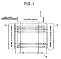
- Fig. 1 is a view schematically showing an arrangement of a PDP driving apparatus including the aforementioned PDP.
- a PDP 1 is provided with row electrodes Y 1 through Y n and row electrodes X 1 through X n , wherein pairs of an electrode X and an electrode Y form row electrode pairs corresponding to respective rows (the first row through the n' th row) in one screen. Further, the PDP 1 is provided with column electrodes D 1 through D m , intersecting at right angles with the row electrode pairs with unillustrated dielectric layer and discharge space in between, that form column electrodes corresponding to respective columns (the first column through the m' th column) in one screen.
- a discharge cell corresponding to one pixel is formed at each intersection portion of each row electrode pair and each column electrode.
- An address driver 2 converts pixel data for each pixel based on a video signal to a pixel data pulse having a voltage value corresponding to its logical level, and applies one row of pixel data pulses to the column electrodes D 1 through D m row by row.
- An X row electrode driver 3 generates a reset pulse for initializing a quantity of residual wall charges in each discharge cell and a sustaining discharge pulse for sustaining a discharge-to-emit light condition of a light emitting discharge cell as will be described below, and applies these pulses to the row electrodes X 1 through X n .
- a Y row electrode driver 4 Like the X row electrode driver 3, a Y row electrode driver 4 generates a reset pulse for initializing a quantity of residual wall charges in each discharge cell and a sustaining discharge pulse for sustaining a discharge-to-emit light condition of a light emitting discharge cell, and applies these pulses to the row electrodes Y 1 through Y n . Further, the Y row electrode driver 4 generates a priming pulse (PP) for allowing charged particles generated within the discharge cell to be formed again and a scanning pulse (SP) for allowing a quantity of charges corresponding to the pixel data pulse to be generated in each discharge cell to set the light emitting discharge cell or a non-luminous discharge cell, and applies these pulses to the row electrodes Y 1 through Y n .
- PP priming pulse
- SP scanning pulse
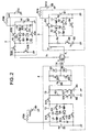
- Fig. 2 shows a concrete arrangement of the X row electrode driver 3, the Y row electrode driver 4, and the address driver 2, wherein the drivers are shown as to an electrode X j , an electrode Y j , and an electrode D i for one pixel.
- the electrode X j is the electrode in the j' th row among the electrodes X 1 through X n
- the electrode Y j is the electrode in the j' th row among the electrodes Y 1 through Y n
- a space between the electrode X j and the electrode Y j functions as a capacitor C0.
- the electrode D i is the electrode in the i' th column among the electrodes D 1 through D m .
- the X row electrode driver 3 is provided with two power sources B1 and B2.
- the power source B1 outputs a voltage V s1 (for example, 170 V), and the power source B2 outputs a voltage V r1 (for example, 190 V).
- the positive terminal of the power source B1 is connected to a connection line 11 to the electrode X j through a switching element S3, and the negative terminal is grounded.
- Connected somewhere between the connection line 11 and the ground are, in addition to a switching element S4, a series circuit composed of a switching element S1, a diode D1, and a coil L1, and another series circuit composed of a coil L2, a diode D2, and a switching element S2 through a common capacitor C1 at the ground side.
- the diode D1 is connected so that its anode is at the capacitor C1 side and the diode D2 is connected so that its cathode is at the capacitor C1 side. Also, the positive terminal of the power source B2 is connected to the connection line 11 through a switching element S8 and a resistor R1, and the negative terminal of the power source B2 is grounded.
- the Y row electrode driver 4 is provided with four power sources B3 through B6.
- the power source B3 outputs a voltage V s1 (for example, 170 V)
- the power source B4 outputs a voltage -V r1 (for example, -190 V)
- the power source B5 outputs a voltage -V off (for example, -10 to -20 V)
- the power source B6 outputs a voltage V h (for example, 160 V, V h > V off ).
- the positive terminal of the power source B3 is connected to a connection line 12 to a switching element S15 through a switching element S13, and the negative terminal is grounded.
- a switching element S14 is connected between the connection line 12 and the ground.
- connection line 12 Also connected between the connection line 12 and the ground are, a series circuit composed of a switching element S11, a diode D3, and a coil L3, and another series circuit composed of a coil L4, a diode D4 and a switching element S12 through a common capacitor C2 at the ground side.
- the diode D3 is connected in a direction that its anode is on the capacitor C2 side and the diode D4 is connected in a direction that its cathode is on the capacitor C2 side.
- connection line 12 is connected to a connection line 13 to the negative terminal of the power source B6 through the switching element S15.
- the positive terminal of the power source B4 is grounded, and the negative terminal is connected to the connection line 13 through a switching element S16 and a resistor R2.
- the negative terminal of the power source B5 is connected to the connection line 13 through a switching element S17, and the positive terminal is grounded.
- connection line 13 is connected to a connection line 14 to the electrode Y j through a switching element S22.
- the positive terminal of the power source B6 is connected to the connection line 14 through a switching element S21.
- a diode D6 is connected somewhere between the connection lines 13 and 14, and a diode D5 is connected somewhere between the positive terminal of the power source B6 and the connection line 14 in parallel.
- the diode D5 is connected in a direction that its anode is on the connection line 14 side, and the diode D6 is connected in a direction that its cathode is on the connection line 14 side.
- the address driver 2 is provided with a power source B7 that outputs a voltage V d (for example, 60 V).
- the positive terminal of the power source B7 is connected to the electrode D i through a switching element S33, a connection line 15, and a switching element S35, and the negative terminal is grounded.
- a switching element S34 is connected between the connection line 15 and the ground.
- a series circuit composed of a switching element S31, a diode D7 and a coil L5, and another series circuit composed of a coil L6, a diode D8, and a switching element S32 through a common capacitor C3 at the ground side.
- the diode D7 is connected in a direction that its anode is on the capacitor C3 side and the diode D8 is connected in a direction that its cathode is on the capacitor C3 side.
- the electrode D i is grounded through a switching element S36.
- the switching elements S35 and S36 operate alternately, and control generation of an address data pulse to be supplied to the capacitor C0 in the discharge cell unit.
- the capacitors C1, C2, and C3 (hereinafter, referred to as the power collecting capacitors) included in the X row electrode driver 3, the Y row electrode driver 4, and the address driver 2, respectively, are connected to power sources B8, B9, and B10 through resistors R10, R20, and R30, respectively, only for a predetermined period upon power-up of the PDP apparatus.
- These power sources charge their respective power collecting capacitors to midpoint potentials of their respective resonance voltages.
- the potentials of the power sources B8 and B9 are half the aforementioned V s1 , that is, V s1 /2, and the potential of the power source B10 is half the aforementioned V d , that is, V d /2.
- the power source B3, the switching elements S11 through S15, the coils L3 and L4, the diodes D3 and D4, and the capacitor C2 form a sustaining driver (sustaining discharge driving);
- the power source B4, the resistor R2, and the switching element S16 form a reset driver; and the rest of the power sources B5 and B6, the switching elements S17, S21, and S22, and the diodes D5 and D6 form a scanning driver (scanning driving).
- the operation of the PDP driving apparatus is mainly composed of a reset period, an address period, and a sustain period.
- the switching element S8 in the X row electrode driver 3 is switched ON, and both the switching elements S16 and S22 in the Y row electrode driver 4 are switched ON. At this point, all the other switching elements stay OFF.
- a peak-to-peak value of the reset pulse PR x becomes the voltage V r1 of the power source B2 in the end, while the peak-to-peak value of the reset pulse PR y becomes the voltage - V r1 of the power source B4.
- the reset pulse PR x is applied to all the electrodes X 1 through X n concurrently, and likewise, the reset pulse PR y is generated for each of the electrodes Y 1 through Y n and applied to all the electrodes Y 1 through Y n concurrently.
- the switching elements S8, S16, and S22 are switched OFF after the reset pulses PR x and PR y reach the saturation level and before the reset period ends. At this point, the switching elements S4, S14, and S15 are switched ON, and both the electrodes X j and Y j are grounded, whereupon the reset pulses PR x and PR y are lost.
- the PDP driving circuit operates as has been described during the reset period.
- the switching elements S14 and S15 are switched OFF and the switching element S17 is switched ON, and at the same time, the switching element S22 is switched ON.
- the switching elements S17 and S22 are switched ON, the negative potential -V off at the negative terminal of the power source B5 is applied to the electrode Y j through the switching element S17 and the switching element S22.
- the address driver 2 converts the pixel data for each pixel based on a video signal to pixel data pulses DP 1 through DP n each having a voltage value corresponding to their respective logical levels, and successively applies one row of the data pulses to the column electrodes D 1 through D m .
- the pixel data pulses DP j and DP j+1 are applied to the electrodes Y j and Y j+1 .
- the Y row electrode driver 4 successively applies the priming pulse (PP) of a positive voltage to the row electrodes Y 1 through Y n . Further, the Y row electrode driver 4 successively applies the scanning pulse (SP) of a negative voltage to the row electrodes Y 1 through Y n immediately after each is applied with the priming pulse (PP) and in synchronism with the timing of each pulse in a group of the pixel data pulses DP 1 through DP n .
- PP priming pulse
- SP scanning pulse
- the switching element S21 is switched ON and the switching element S22 is switched OFF when the priming pulse (PP) is generated.
- the resulting positive potential is applied to the electrode Y j through the switching element S21 as the priming pulse (PP).
- the switching pulse S21 is switched OFF in synchronism with the application of the pixel data pulse DP j from the address driver 2, whereupon the switching element S22 is switched ON. Consequently, the negative potential -V off at the negative terminal of the power source B5 is applied to the electrode Y j through the switching element S17 and then the switching element S22 as the scanning pulse (SP). Subsequently, the switching element S21 is switched ON at the same time when the application of the pixel data pulse DP j from the address driver 2 is stopped, whereupon the switching element S22 is switched OFF.
- the potential (V h - V off ) at the positive terminal of the power source B6 is applied to the electrode Y j through the switching element S21.
- the priming pulse (PP) is applied to the electrode Y j+1 in the (j+1)' th row in the same manner as the electrode Y j
- the scanning pulse (SP) is applied in synchronism with the application of the pixel data pulse DP j+1 from the address driver 2.
- the discharge cells belonging to the row electrodes to which the scanning pulse (SP) is applied those to which the pixel data pulse DP of a positive voltage is applied concurrently will start to discharge, so that these discharge cells lose most of the wall charges.
- the discharge cells to which the scanning pulse (SP) is applied but the pixel data pulse of a positive voltage is unapplied will not start to discharge, so that these discharge cells hold the residual wall charges.
- the discharge cells holding the residual wall charges become the light emitting discharge cells, and the discharge cells having lost the wall charges become the non-luminous discharge cells.
- the PDP driving circuit operates as has been described during the address period.
- the switching elements S17 and S21 are switched OFF, and in turn, the switching elements S14 and S15 are switched ON when the address period shifts to the sustain period.
- the switching element S4 stays ON since the preceding address period, and the potential of the electrode X j is the ground potential at almost 0 V. Then, the switching element S4 is switched OFF, and the switching element S1 is switched ON, whereupon a current reaches the electrode X j through the coil L1, the diode D1, and the switching element S1 due to the charges accumulated in the capacitor C1, and the current flows into the capacitor C0, whereby the capacitor C0 is charged.
- the potential of the electrode X j increases gradually because of a time constant of the coil L1 and the capacitor C0.
- the switching element S1 is switched OFF, and the switching element S3 is switched ON. Consequently, the potential V s1 at the positive terminal of the power source B1 is applied to the electrode X j . Subsequently, the switching element S3 is switched OFF, and the switching element S2 is switched ON, whereupon a current flows into the capacitor C1 from the electrode X j through the coil L2, the diode D2, and the switching element S2 due to the charges accumulated in the capacitor C0.
- the potential of the electrode X j decreases gradually because of a time constant of the coil L2 and the capacitor C1.
- the switching element S2 is switched OFF, and the switching element S4 is switched ON, whereupon the capacitor C0 is grounded.
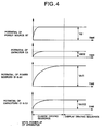
- the X row electrode driver 3 applies a sustaining discharge pulse IP x of a positive voltage as shown in Fig. 3 to the electrode X j .
- the switching element S11 is switched ON and the switching element S14 is switched OFF concurrently.
- the potential of the electrode Y j is the ground potential at almost 0 V while the switching element S14 stays ON.
- a current reaches the electrode Y j through the coil L3, the diode D3, the switching element S11, the switching element S15, and the diode D6 due to the charges accumulated in the capacitor C2, and the current flows into the capacitor C0, whereby the capacitor C0 is charged.
- the potential of the electrode Y j increases gradually because of a time constant of the coil L3 and the capacitor C0.
- the switching element S11 is switched OFF and the switching element S13 is switched ON. Consequently, the potential V s1 at the positive terminal of the power source B3 is applied to the electrode Y j through the switching element S13, the switching element S15, and the diode D6. Subsequently, the switching element S13 is switched OFF and the switching element S12 is switched ON, and further, the switching element S22 is switched ON. Consequently, a current flows into the capacitor C2 from the electrode Y j through the switching element S22, the switching element S15, the coil L4, the diode D4, and the switching element S12 due to the charges accumulated in the capacitor C0. At this point, as shown in Fig.
- the potential of the electrode Y j decreases gradually because of a time constant of the coil L4 and the capacitor C2.
- the switching elements S12 and S22 are switched OFF and the switching element S14 is switched ON.
- the Y row electrode driver 4 applies a sustaining discharge pulse IP y of a positive voltage as shown in Fig. 3 to the electrode Y j .
- the sustaining discharge pulse IP x and the sustaining discharge pulse IP y are generated alternately, and respectively applied to the electrodes X 1 through X n and the electrodes Y 1 through Y n alternately.
- the light emitting discharge cells holding the residual wall charges repeat the discharge to emit light with the application of the sustaining discharge pulse voltage, thereby sustaining the light emitting condition.
- the power collecting capacitors (C1 through C3) in their respective resonance drivers shown in Fig. 2 it is necessary to charge the power collecting capacitors (C1 through C3) in their respective resonance drivers shown in Fig. 2 to predetermined potentials upon power-up of the apparatus before the display driving sequence starts.
- the aforementioned display driving sequence is started while the potentials of these capacitors are 0, the operation may possibly cause a problem because of a potential difference within the resonance circuits.
- all the resonance drivers are provided with the power sources B8 through B10, respectively, for charging the power collecting capacitors, and the respective capacitors C1 through C3 are charged directly to the midpoint potentials (V s1 /2 or V d /2) of the resonance voltages from these power sources through the resistors R10, R20, and R30, respectively.
- the capacitors need to be charged through a series resistor having a relatively large resistance value to control a rush current upon power-up of the apparatus.
- the charging of these capacitors is time-consuming, and it takes a time until an image is displayed by shifting to the normal display driving sequence since the power-up of the apparatus.
- the present invention provides a driving apparatus of a light emitting display panel having a capacitive load and capable of charging power collecting capacitors included in respective resonance driver circuits to predetermined potentials safely at high speeds by solving the problems described above.
- the present invention provides a driving apparatus for driving a display panel, having a plurality of row electrode pairs and a plurality of column electrodes aligned to intersect with the row electrode pairs in forming a light emitting display cell at each intersection portion, to emit light by including a plurality of driving circuits for selectively supplying light-emitting-display driving pulses to the row electrode pairs and the column electrodes through an output terminal, wherein: each of the driving circuits includes a switch circuit for forming a forward/reverse current path alternatively between the output terminal and a power collecting capacitive element through an inductance element, and has a switching resonance charge/discharge circuit for performing generation of the driving pulses; and the switch circuit performs a switching operation not only during a light emitting display operation, but also upon power-up.
- the switch circuit in each of the first driving circuits performs the switching operation in synchronism with each other; and the power collecting capacitive element in each of the first driving circuits is charged to a midpoint potential of a resonance voltage.
- the switch circuit in the second driving circuit performs the switching operation alternately with the switching operation by the first driving circuits; and the power collecting capacitive element in the second driving circuit is charged to the midpoint potential of the resonance voltage.
- a PDP driving apparatus of the present invention performs the so-called charge driving sequence to charge each power collecting capacitor included in their respective driver circuits to a predetermined potential for each of the display pixels of the PDP upon power-up of the apparatus.
- the address driver 2 charges the capacitor C3 to half the potential of the power source B7, that is, V d /2
- the X row electrode driver 3 and the Y row electrode driver 4 respectively charge the capacitors C1 and C2 to half the potentials of the power sources B1 and B3, that is, V s1 /2.
- the PDP driving apparatus of the present invention after the PDP driving apparatus performs the charge driving sequence, it shifts to the aforementioned normal display driving sequence composed of the reset period, address period, and sustain period.
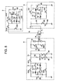
- Fig. 5 is a circuit diagram showing an arrangement of a driving circuit for one pixel in the PDP 1 of the PDP driving apparatus of the present invention. Like components are labeled with like reference numerals with respect to Fig. 2 for ease of explanation.
- the circuitry shown in Fig. 5 omits the charge circuits (power sources B8 through B10 and the resistors R10, R20, and R30) for the power collecting capacitors (C1 through C3) in their respective resonance drivers activated upon power-up from the circuit arrangement shown in Fig. 2, and because the other arrangements are the same, an explanation of each portion in the circuit is omitted.
- the column electrode circuit is excited by applying a charge driving pulse to the column electrode D i in the first place, which will be described more in detail in the following.
- the switching element S36 is switched OFF, and the switching element S35 is switched ON. Consequently, the condition is prepared for applying a charge driving pulse to the column electrode D i from the address driver 2.
- the switching element S34 is switched OFF and the switching element S31 is switched ON, whereupon a current reaches the electrode D i through the coil L5, the diode D7 and the switching element S31 due to the charges accumulated in the capacitor C3, and the current flows into a capacitive load formed between the column electrode D i and the corresponding discharge cell, whereby the capacitive load is charged.
- the potential of the electrode Di increases gradually because of a time constant of the coil L5 and the capacitive load.
- the switching element S31 is switched OFF and the switching element S33 is switched ON. Consequently, the potential V d at the positive terminal of the power source B7 is applied to the electrode D i . Subsequently, the switching element S33 is switched OFF and the switching element S32 is switched ON, whereupon a current flows into the capacitor C3 from the electrode D i through the coil L6, the diode D8, and the switching element S32 due to the charges accumulated in the capacitive load between the column electrode D i and the discharge cell.
- the potential of the electrode D i decreases gradually because of a time constant of the coil L6 and the capacitor C3.
- the switching element S32 is switched OFF and the switching element S34 is switched ON, whereupon the capacitive load between the column electrode D i and the discharge cell is grounded.
- the address driver 2 applies a charge driving pulse Dp of a positive voltage as shown in Fig. 6 to the electrode D i .
- the charges accumulated in the capacitor C3 immediately after the power-up of the apparatus are 0 or have an extremely slight quantity, so that an increase in the potential of the charge driving pulse Dp is an extremely small value.
- the amplitude of the charge driving pulse applied to the electrode D i with a power supply from the power source B7 increases abruptly while the excitation driving is repeated, and accordingly, so does the charge potential of the capacitor C3.
- the switching element S34 is switched ON and the potential of the column electrode D i decreases to almost 0, the switching element S35 is switched OFF and the switching element S36 is switched ON, whereupon the address driver 2 is disconnected from the electrode D i .
- the switching element S4 stays ON and the potential of the electrode X j is the ground potential at almost 0 V.
- the switching element S4 is switched OFF and the switching element S1 is switched ON. Consequently, a current reaches the electrode X j through the coil L1, the diode D1, and the switching element S1 due to the charges accumulated in the capacitor C1, and the current flows into the capacitor C0 in the discharge cell, whereby the capacitor C0 is charged.
- the potential of the electrode X j increases gradually because of a time constant of the coil L1 and the capacitor C0.
- the switching element S1 is switched OFF and the switching element S3 is switched ON. Consequently, the potential V s1 at the positive terminal of the power source B1 is applied to the electrode X j . Subsequently, the switching element S3 is switched OFF and the switching element S2 is switched ON, whereupon a current flows into the capacitor C1 from the electrode X j through the coil L2, the diode D2, and the switching element S2 due to the charges accumulated in the capacitor C0.
- the potential of the electrode X j decreases gradually because of a time constant of the coil L2 and the capacitor C1.
- the switching element S2 is switched OFF and the switching element S4 is switched ON, whereupon the capacitor C0 is grounded.
- the X row electrode driver 3 applies a charge driving pulse IP x of a positive voltage as shown in Fig. 6 to the electrode X j .
- the switching element S14 is switched OFF at the same time the switching element S4 in the X row electrode driver 3 is switched OFF. Then, the switching element S11 is switched ON in synchronism with the switching ON of the switching element S1 in the X row electrode driver 3.
- the potential of the electrode Y j is the ground potential at almost 0 V while the switching element S14 stays ON.
- the switching element S11 is switched OFF and the switching element S13 is switched ON in synchronism with the movements of the switching elements S1 and S3 in the X row electrode driver 3. Consequently, the potential V s1 at the positive terminal of the power source B3 is applied to the electrode Y j through the switching element S13, the switching element S15, and the diode D6.
- the switching element S13 is switched OFF and the switching element S12 is switched ON, and further, the switching element S22 is switched ON in synchronism with the movements of the switching elements S3 and S2 in the X row electrode driver 3. Consequently, a current flows into the capacitor C2 from the electrode Y j through the switching element S22, the switching element S15, the coil L4, the diode D4, and the switching element S12 due to the charges accumulated in the capacitor C0.
- the potential of the electrode Y j decreases gradually because of a time constant of the coil L4 and the capacitor C2.
- the switching elements S12 and S22 are switched OFF and the switching element S14 is switched ON.
- the Y row electrode driver 4 applies a charge driving pulse IP y of a positive voltage as shown in Fig. 6 to the electrode Y j .
- the charge driving pulses IP x and IP y respectively applied to the electrode X j and the electrode Y j have pulse waveforms in synchronism with each other over time.
- the charge driving pulses IP x and IP y respectively applied to the electrode X j and the electrode Y j of the capacitor C0 are in-phase pulses of the same polarity, and therefore, a potential difference between the electrode X j and the electrode Y j does not vary.
- no discharge occurs between the electrode X j and the electrode Y j of the capacitor C0 during the charge driving sequence, and naturally, no light is emitted erroneously in the discharge cell of the capacitor C0.
- the charges accumulated in the capacitors C1 and C2 immediately after the power-up of the apparatus are 0 or have an extremely slight quantity, so that an increase in the potential of the charge driving pulses IP x and IP y is an extremely small value.
- the amplitude of the charge driving pulses applied to the electrode X j and the electrode Y j with power supplies from the power sources B1 and B3 increases abruptly while the excitation driving is repeated, and accordingly, so does the charge potential of each of the capacitors C1 and C2.
- the foregoing operations of the address driver 2, the X row electrode driver 3, and the Y row electrode driver 4 are repetitively performed during the charge driving sequence.
- a control circuit (not shown) in the PDP driving apparatus terminates the charge driving sequence, and shifts to the aforementioned normal display driving sequence.
- the control circuit may, for example, monitor the potential in each capacitor directly with a high impedance potential sensor.
- a time constant during the charge and a duty cycle of the charge driving pulse are known, it is possible to pre-compute an increase in the potential by the excitation driving.
- the termination of the charge driving sequence may be judged by a predetermined timer the control circuit has set.
- the embodiment described above shows a case where a resonance driver circuit is used for each of the column electrode driving circuit and the row electrode pair driving circuit in the PDP driving circuit. It should be appreciated, however, that the present invention is not limited to the foregoing. For example, the present invention is applicable to a case where a resonance driver circuit is used for the row electrode pair driving circuit alone.
- the charge driving pulses in-phase and of the same polarity are repetitively applied to the electrode X and the electrode Y in the row electrode pair for a certain period of time, so that the power collecting capacitive elements included in their respective resonance drivers, that is, the capacitors C1 and C2, are charged to the midpoint potential V s1 /2 between the high potential V s1 and the low potential 0 during the resonance.
- the present embodiment shows a case where a PDP is used as a display panel having a capacitive light emitting load. It should be appreciated, however, that the present invention is not limited to the foregoing. It is needless to say that the present invention can be applied to any display panel having a capacitive light emitting load, for example, an EL display apparatus.
- the present invention it is possible to charge the power collecting capacitive element, which is included in the resonance driver in a light-emitting display panel driving apparatus having a capacitive load, to a predetermined potential almost concurrently with the power-up of the apparatus through excitation by the resonance driver. Hence, it is possible to drastically shorten a time required to display an image by shifting to the normal display driving sequence since the power-up of the driving apparatus.
- the row electrode pairs in the driving apparatus are excited by the charge driving pulses in-phase and of the same polarity during the charge driving sequence by the resonant driver. Hence, hardly any light is emitted erroneously in the discharge cell during the charge driving sequence.
Landscapes
- Engineering & Computer Science (AREA)
- Power Engineering (AREA)
- Physics & Mathematics (AREA)
- Plasma & Fusion (AREA)
- Computer Hardware Design (AREA)
- General Physics & Mathematics (AREA)
- Theoretical Computer Science (AREA)
- Control Of Indicators Other Than Cathode Ray Tubes (AREA)
- Control Of Gas Discharge Display Tubes (AREA)
- Control Of El Displays (AREA)
Abstract
Description
Claims (5)
- A driving apparatus of a display panel for driving said display panel, having a plurality of row electrode pairs and a plurality of column electrodes aligned to intersect with said row electrode pairs in forming a light emitting display cell at each intersection portion, to emit light by including a plurality of driving circuits for selectively supplying light-emitting-display driving pulses to said row electrode pairs and said column electrodes through an output terminal, wherein:each of said driving circuits includes a switch circuit for forming a forward/reverse current path alternatively between said output terminal and a power collecting capacitive element through an inductance element, and has a switching resonance charge/discharge circuit for performing generation of said driving pulses; andsaid switch circuit performs a switching operation not only during a light emitting display operation, but also upon power-up.
- The driving apparatus of a display panel according to claim 1, wherein, of said driving circuits, as to a pair of first driving circuits connected to each of said row electrode pairs:said switch circuit in each of said first driving circuits performs the switching operation in synchronism with each other upon power-up; andsaid power collecting capacitive element in each of said first driving circuits is charged to a midpoint potential of a resonance voltage by said switching operation.
- The driving apparatus of a display panel according to claim 2, wherein, of said driving circuits, as to a second driving circuit connected to said column electrodes:said switch circuit in said second driving circuit performs the switching operation alternately with the switching operation by said first driving circuits upon power-up; andsaid power collecting capacitive element in said second driving circuit is charged to the midpoint potential of the resonance voltage by said switching operation.
- The driving apparatus of a display panel according to any one of claims 1 through 3,
wherein said inductance element is composed of first and second inductance elements each connected to a different current path in said forward/reverse current path, and
said switch circuit includes:first potential transfer means for transferring a potential of an electrode connected to said driving circuit from a first potential to a second potential by resonance between said first inductance element and the capacitive load that said light emitting display cell has;power supplying means for supplying power to said capacitive load;second potential transfer means for transferring the potential of the electrode connected to said driving circuit from the second potential to the first potential by resonance between said second inductance element and the capacitive load; andpower collecting means for collecting power from said capacitive load to said power collecting capacitive element. - A driving apparatus of a display panel including a display panel provided with a plurality of light emitting display cells each having a capacitive load, and a light emitting driving circuit for selecting said light emitting display cells and supplying a light emitting driving pulse to said selected cells through an output terminal, wherein:said light emitting driving circuit includes a switch circuit for forming a forward/reverse current path alternatively between said output terminal and a power collecting capacitive element through an inductance element, and has a switching resonance charge/discharge circuit for performing generation of said light emitting driving pulses; andsaid switch circuit performs a switching operation not only during a light emitting display operation, but also upon power-up.
Applications Claiming Priority (2)
| Application Number | Priority Date | Filing Date | Title |
|---|---|---|---|
| JP2001179900 | 2001-06-14 | ||
| JP2001179900A JP4660020B2 (en) | 2001-06-14 | 2001-06-14 | Display panel drive device |
Publications (2)
| Publication Number | Publication Date |
|---|---|
| EP1267320A2 true EP1267320A2 (en) | 2002-12-18 |
| EP1267320A3 EP1267320A3 (en) | 2007-02-28 |
Family
ID=19020393
Family Applications (1)
| Application Number | Title | Priority Date | Filing Date |
|---|---|---|---|
| EP02011641A Withdrawn EP1267320A3 (en) | 2001-06-14 | 2002-05-29 | Driving apparatus of display panel |
Country Status (3)
| Country | Link |
|---|---|
| US (1) | US6922180B2 (en) |
| EP (1) | EP1267320A3 (en) |
| JP (1) | JP4660020B2 (en) |
Cited By (5)
| Publication number | Priority date | Publication date | Assignee | Title |
|---|---|---|---|---|
| EP1480194A3 (en) * | 2003-05-22 | 2006-03-22 | LG Electronics, Inc. | Energy recovery circuit and driving method thereof |
| EP1657705A3 (en) * | 2004-11-08 | 2006-07-26 | LG Electronics, Inc. | Plasma display apparatus and driving method thereof |
| EP1816633A3 (en) * | 2006-02-07 | 2008-06-25 | LG Electronics Inc. | Plasma display apparatus and driving method of plasma display apparatus |
| CN100433095C (en) * | 2005-08-26 | 2008-11-12 | 中华映管股份有限公司 | Method for reducing energy consumption of plasma display |
| EP1699037A3 (en) * | 2005-03-03 | 2009-08-12 | St Microelectronics S.A. | Drive circuit for a plasma display apparatus |
Families Citing this family (9)
| Publication number | Priority date | Publication date | Assignee | Title |
|---|---|---|---|---|
| JP2004177815A (en) * | 2002-11-28 | 2004-06-24 | Fujitsu Hitachi Plasma Display Ltd | Capacitive load drive and recovery circuit,capacitive load drive circuit, and plasma display apparatus using the same |
| JP4430878B2 (en) * | 2003-03-11 | 2010-03-10 | パナソニック株式会社 | Capacitive load drive |
| JP2005043413A (en) * | 2003-07-22 | 2005-02-17 | Pioneer Electronic Corp | Driving method of display panel |
| KR100551051B1 (en) * | 2003-11-27 | 2006-02-09 | 삼성에스디아이 주식회사 | Driving Method of Plasma Display Panel and Plasma Display Device |
| KR100680709B1 (en) * | 2004-12-23 | 2007-02-08 | 엘지전자 주식회사 | Driving device of plasma display panel |
| JP4550696B2 (en) * | 2005-08-31 | 2010-09-22 | 株式会社東芝 | Liquid crystal display control apparatus and liquid crystal display control method |
| CN100545991C (en) * | 2005-11-11 | 2009-09-30 | 中华映管股份有限公司 | Plasma display panel and driving method |
| US20080150438A1 (en) * | 2006-12-20 | 2008-06-26 | Yoo-Jin Song | Plasma display and driving method thereof |
| CN119232183B (en) * | 2024-08-30 | 2025-11-07 | 荣耀终端股份有限公司 | Signal transmitting circuit, wireless communication module and electronic equipment |
Family Cites Families (6)
| Publication number | Priority date | Publication date | Assignee | Title |
|---|---|---|---|---|
| US4866349A (en) * | 1986-09-25 | 1989-09-12 | The Board Of Trustees Of The University Of Illinois | Power efficient sustain drivers and address drivers for plasma panel |
| JP2755201B2 (en) * | 1994-09-28 | 1998-05-20 | 日本電気株式会社 | Drive circuit for plasma display panel |
| JP2715939B2 (en) * | 1994-11-08 | 1998-02-18 | 日本電気株式会社 | Display panel drive circuit |
| JP3526179B2 (en) * | 1997-07-29 | 2004-05-10 | パイオニア株式会社 | Plasma display device |
| JP3036496B2 (en) * | 1997-11-28 | 2000-04-24 | 日本電気株式会社 | Driving method and circuit for plasma display panel and plasma display panel display |
| US6567059B1 (en) * | 1998-11-20 | 2003-05-20 | Pioneer Corporation | Plasma display panel driving apparatus |
-
2001
- 2001-06-14 JP JP2001179900A patent/JP4660020B2/en not_active Expired - Fee Related
-
2002
- 2002-05-28 US US10/154,926 patent/US6922180B2/en not_active Expired - Fee Related
- 2002-05-29 EP EP02011641A patent/EP1267320A3/en not_active Withdrawn
Cited By (8)
| Publication number | Priority date | Publication date | Assignee | Title |
|---|---|---|---|---|
| EP1480194A3 (en) * | 2003-05-22 | 2006-03-22 | LG Electronics, Inc. | Energy recovery circuit and driving method thereof |
| US20070109229A1 (en) * | 2003-05-22 | 2007-05-17 | Kwak Jong W | Energy recovery circuit and driving method thereof |
| US7403199B2 (en) | 2003-05-22 | 2008-07-22 | Lg Electronics Inc. | Energy recovery circuit and driving method thereof |
| EP1657705A3 (en) * | 2004-11-08 | 2006-07-26 | LG Electronics, Inc. | Plasma display apparatus and driving method thereof |
| US7598932B2 (en) | 2004-11-08 | 2009-10-06 | Lg Electronics Inc. | Plasma display apparatus and driving method thereof |
| EP1699037A3 (en) * | 2005-03-03 | 2009-08-12 | St Microelectronics S.A. | Drive circuit for a plasma display apparatus |
| CN100433095C (en) * | 2005-08-26 | 2008-11-12 | 中华映管股份有限公司 | Method for reducing energy consumption of plasma display |
| EP1816633A3 (en) * | 2006-02-07 | 2008-06-25 | LG Electronics Inc. | Plasma display apparatus and driving method of plasma display apparatus |
Also Published As
| Publication number | Publication date |
|---|---|
| US6922180B2 (en) | 2005-07-26 |
| EP1267320A3 (en) | 2007-02-28 |
| JP2002372946A (en) | 2002-12-26 |
| JP4660020B2 (en) | 2011-03-30 |
| US20020190928A1 (en) | 2002-12-19 |
Similar Documents
| Publication | Publication Date | Title |
|---|---|---|
| US6680581B2 (en) | Apparatus and method for driving plasma display panel | |
| US7193586B2 (en) | Apparatus and methods for driving a plasma display panel | |
| EP1187088A2 (en) | Driving apparatus for driving display panel | |
| US6922180B2 (en) | Driving apparatus of display panel | |
| JP3568098B2 (en) | Display panel drive | |
| US7133006B2 (en) | Display panel drive apparatus | |
| US6833824B2 (en) | Driving method for plasma display panel | |
| KR20050051824A (en) | Plasma display device and driving method of plasma display panel | |
| JP3556108B2 (en) | Driving method of PDP | |
| US6567059B1 (en) | Plasma display panel driving apparatus | |
| JP3591766B2 (en) | PDP drive | |
| JP2000293135A (en) | Driving device for plasma display panel | |
| US7605781B2 (en) | Display panel driving method | |
| JP3678333B2 (en) | Display panel drive device | |
| JP2005025153A (en) | Apparatus for driving capacitive light emitting element | |
| US20060077133A1 (en) | Plasma display device and driving method thereof | |
| KR100870331B1 (en) | Plasma display device and driving method thereof | |
| US20050219155A1 (en) | Driving method of display panel | |
| KR100740093B1 (en) | Plasma Display, Driving Device and Driving Method | |
| KR100570612B1 (en) | Driving apparatus for plasma display panel and driving method thereof | |
| KR100627410B1 (en) | Plasma display device and driving method thereof | |
| US20050200565A1 (en) | Method for driving display panel | |
| JP2007279143A (en) | Display device | |
| US20080122374A1 (en) | Plasma display device and driving method thereof | |
| JP2005182074A (en) | Driving device for display panel |
Legal Events
| Date | Code | Title | Description |
|---|---|---|---|
| PUAI | Public reference made under article 153(3) epc to a published international application that has entered the european phase |
Free format text: ORIGINAL CODE: 0009012 |
|
| AK | Designated contracting states |
Kind code of ref document: A2 Designated state(s): AT BE CH CY DE DK ES FI FR GB GR IE IT LI LU MC NL PT SE TR |
|
| AX | Request for extension of the european patent |
Free format text: AL;LT;LV;MK;RO;SI |
|
| RAP1 | Party data changed (applicant data changed or rights of an application transferred) |
Owner name: PIONEER DISPLAY PRODUCTS CORPORATION Owner name: PIONEER CORPORATION |
|
| PUAL | Search report despatched |
Free format text: ORIGINAL CODE: 0009013 |
|
| AK | Designated contracting states |
Kind code of ref document: A3 Designated state(s): AT BE CH CY DE DK ES FI FR GB GR IE IT LI LU MC NL PT SE TR |
|
| AX | Request for extension of the european patent |
Extension state: AL LT LV MK RO SI |
|
| RIC1 | Information provided on ipc code assigned before grant |
Ipc: G09G 3/288 20060101AFI20070125BHEP |
|
| 17P | Request for examination filed |
Effective date: 20070713 |
|
| AKX | Designation fees paid |
Designated state(s): DE FR GB |
|
| 17Q | First examination report despatched |
Effective date: 20071108 |
|
| STAA | Information on the status of an ep patent application or granted ep patent |
Free format text: STATUS: THE APPLICATION IS DEEMED TO BE WITHDRAWN |
|
| 18D | Application deemed to be withdrawn |
Effective date: 20080319 |